used to implement a proprietary bus protocol. For example, it is possible to use one of the FT2232H’s channels to connect to an SRAM configurable FPGA such as supplied by Altera or Xilinx. The FPGA device would normally be un-configured (i.e. have no defined function) at power-up. Application software
of thousands of hours. A particular de- Cree’s Application Engineering group tested four different vice could be subjected to repeated transients at an am- types of XLamp LEDs at pulsed currents over a broad range plitude some percentage above the
LOL, da ist ja wirklich so ein DIP Riesenkäfer drin, gibt's auch als PC-Steckkarte, da ist der Prozessor fast so hoch wie die ganze Steckkarte. Irgendwie würde es mich auch reizen, nochmal ein Minimal-System mit diesem Riesenkäfer aufzubauen, aber das wäre
-N auf Demo-Paltine mit 74HCT573 + 2 x 28pol. Die hatte ich als Emulator für 8031 und AT89C2051 verwendet. > 10 x 8kB-CMOS-RAM Seinerzeit hatte ich einen PEPS-ROM-Emulator, der an LPT1 betrieben wurde. Affenschnell. Heute gibt es hoffentlich etwas Ähnliches mit USB-Anschluß.
dBVrms Local Oscillator Jitter 100 Hz – 100 kHz 0.3 º rms Notes: 1) Matched to 1 k source 2) Two tones at 2.3 MHz & 3.8 MHz each of 33 mVp-p, balanced input. LO1 at 130 MHz, LO2 at 132.55 MHz, IM2 products at 450 kHz at I/Q outputs 3) Two tones at 2.3 MHz & 3.8 MHz each of 0.33 Vp-p, balanced input. LO1
pro Stück gibt. Einzeln 1,52 €. Peter D. schrieb im Beitrag #7830526: > Ich hatte zuerst mit 80C51 angefangen, konkret AT89C2051. ... Peter D. (peda) schlägt den AT89C2051 vor. Sieht interessant aus. Da werde ich mal prüfen, wie ich ein Programm aufspielen würde. Ich will eigentlich keine Programmier-Hardware
oder AT89LP51RD2 und der Wickenhäuser und SDCC sollen wohl auch recht guten Code erzeugen.
Uwe S. schrieb im Beitrag #7829062: > degeneriert > dumm > alles F*tzen außer Mutti... Uwe S. schrieb im Beitrag #7829062: > Zinkchlorid Tolle Idee: https://chemicalsafety-ilo-org.translate.goog/
Kilo S. schrieb im Beitrag #7828996: > Stephan S. schrieb im Beitrag #7828953: >> Maus am USB-Anschluss und schon geht die Eingabe. > > Nicht immer, muss dazu OTG fähig sein. Naja, das ist dann aber
CCMAX 2 Note 15: The DS1308 can detect any single SCL clock held low longer thTIMEOUTMIN . The device’s I C interface is in reset state and can receive a new START condition when SCL is held low for at lTIMEOUTMAX . Once the part detects this condition the SDA output is released. The oscillator must be
complete. All products are sold subject to TI’s terms and conditions of sale supplied at the time of order acknowledgment. TI warrants performance of its hardware products to the specifications applicable at the time of sale in accordance with TI’
at CC = 3.3 V,ISO= 5 V ) 60 ICC (mA) at CC= 3.3 V,ISO= 5 V A A ( 80 ( 50 n 70 n r r c 60 C 40 l 50 l p p 30 S 40 u 30 S 20 20 10 10 0 0 0 25 50 75 100 0 25 50 75 100 Data Rate (Mbps) Data Rate (Mbps) CL
THD (VIN– 0.5 dBFS at 1 kHz) All input ranges –102 dB B Input range = ±2.5 REF 89 91.5 dB A Input range = ±1.25 REF 88.5 91 dB A Signal-to-noise ratio SINAD (VIN– 0.5 dBFS at 1 kHz) Input range = ±0.625 REF 87 89 dB A Input
Neue Ver- Frequen arit erk Service PCR Video Symbol- Netzwerk Netzwerk Pos Sendername schlüss z (MHz) ät Satellit (ONID) TS ID ID PID PID rate Name Betreiber Anbieter 1 Das Erste HD 11493 H Astra 1 1 1019 10301 5101 5101 21999SES/AstraSES/Astra ARD Unchecked 2 Das Erste Unchecked11837 H Astra 1 1 1101 28106
LNK6X3/4 440 520 DRAIN Supply FB Voltage = VFBth0.1, mA Current I Switch ON-Time = t LNK6X5 480 560 S2 ON (MOSFET Switching at fOSC LNK6X6 520 600 LNK6X3/4 -5.0 -3.4 -1.8 ICH1 V BP= 0 V BYPASS Pin LNK6X5/6 -7.0 -4.8 -2.5 Charge Current mA LNK6X3/4 -4.0 -2.3 -1.0 ICH2 V BP= 4 V LNK6X5/6 -5.6 -3.2 -1.4
Then, for estimating C DL , the inverse of (19) is calculated as: 1 1 ZF(w) = RCT+ Zw(jw)+ jwC DL = s s + jwC DL RCT+ pw▯ jpw (51) RCT+ pw+ jpw = ▯ s ▯2 s2 + jwC DL RCT+ pw + w Hence, ▯ ▯ ps 1 w Im Z (w ) = ▯ ▯2 2 + wC DL (52) F R CT + ps + sw w Energies 2022, 15, 9251 13 of 26 and by substituting the
601 V DRM Repetitive peak off-state - 500 600 V voltages I RMS on-state current full sine wave; T ≤51 ˚C - 1 A T(RMS) lead ITSM Non-repetitive peak full sine wave;jT = 25 ˚C prior to on-state current surge t = 20 ms - 16 A 2 2 t = 16.7 ms - 17.6 2 I t I t for fusing t = 10 ms - 1.28 A s dIT/dt Repetitive
| Jürgen (oj_k) | 1 | DE | mit Gehäuse, vorzugsweise v2 | spaceman | 2 | AT | n/a | Sascha S. (dec) | 2 | DE | [/c] Vielen Dank
| Jürgen (oj_k) | 1 | DE | mit Gehäuse, vorzugsweise v2 | spaceman | 2 | AT | n/a | Sascha S. (dec) | 2 | DE | | Rainer M. | 2 | DE | mit Gehäuse, vorzugsweise v2 [/c] Gruß Rainer
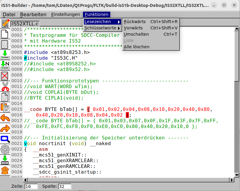
das ich mir dazu bisher angesehen habe geht einzig die MCU51Ide in die richtige Richtung, ist aber weit vom Ziel entfernt. Die Entwicklung von MCU51 ist seit Jahren abgeschlossen, da wird sich auch nichts mehr ändern. Tom
zu > übertragen. Debugger und Programmiertools gibt es nicht herstellerübergreifend. Ein Atmel AT89S2051 wird anders programmiert und debuggt als ein Siemens C515 oder Intel 8032. Und einen Debugger wirst du wohl auch nicht selber schreiben wollen. Das machen die großen IDE auch nicht. Statt dessen
R714 N R702 C706 0R05 4A 1/4W F L703 Q701 100K 1% U706 5 R722 0R05 220NF 16V 1 8 TPS54428DDAR V 2 S D 7 9 3.3uH 3 S D 6 1 E-PAD 8 R706 4 S D 5 2 EN VIN 7 G D 3 VFB VBST 6 C743 100NF 16V C721 C746 C722 51K 1/16W 5% VREG5 SW 0 2 2 AO4449 -7A/-30V 4 SS GND 5 C724 N U U R704 D702 +C707 2 R720 F F F PWR_ON
the beam at a constant frequency. The drive loop's design was facilitated by describing function analysis. The drive loop vibrated the beam at its mechanical resonance because at that frequency, the displacement
devices, and is connected to the internal potentiome- interface as well as the High Voltage Command pin. At ter’s terminal A. the device’s POR/BOR, the value of the A0 address bit The potentiometer’s terminal A is the fixed connection is latched. This input, along with the A2 and A1 pins, to the Full-Scale
prior written approval of an Officer of SMSC and further testing and/or modification will be fully at the risk of the customer. Copies of this document or other SMSC literature, as well as the Terms of Sale Agreement, may be obtained by visiting SMSC’s website at http://www.smsc.com. SMSC is a registered
The DC/DC converter must therefore also be able to generate/provide a positive or a negative voltage at the output. Figure 17 { Power multiplexer structure Power Multiplexer and Accumulator Cells A1 A2 A3 A4 A5 A6 A16 A17 A18 S1 S2 S3 S4 S5 S6 S7 S16 S17 S18 S19 L1 L2 Source: by the author The most important
können zur Reparatur von historischen Geräten dienen (Computern, Messgeräten, Arcade-Maschinen, Synth's etc). Da einige mittlerweile schlecht erhältlich sind, käme es mir frevelhaft vor, die Sammlung in den Elektroschrott zu werfen. Daher biete ich das Konvolut hier an (nur komplett). Linker Block: - D70208L-10 (V40 von NEC) - MAF8039HL (8048-MCU von Philips) - AT89C2051 (Low-Pin-Count-8051 von Atmel) - TS68008CP8 (68k-CPU von ST) - Z8400AB1 (Z80A-CPU von SGS) - SAB8086P (8086-CPU von Siemens) - SAB8088-P (8088-CPU von Siemens) - D87C51FA (8051-MCU mit EPROM
D504 D507 D510 D513 D516 1 0 0 4 4 4 4 0 0 0 0 0 0 C 5 5 5 5 K K R K R R R 51SS355 51SS355 51SS355 51SS355 51SS355 51SS355 P 5 5 R R 1 1 P 1 P P P S S S S S S M3.3V 1 R R P P P0P5010K P0D5010A P0P5040KP0D5040A PPD5070K P0D5070A P0P5100K P0D5100A PPD5130K P0D5130A P0P5160K P0D5160A
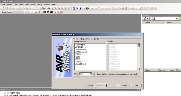
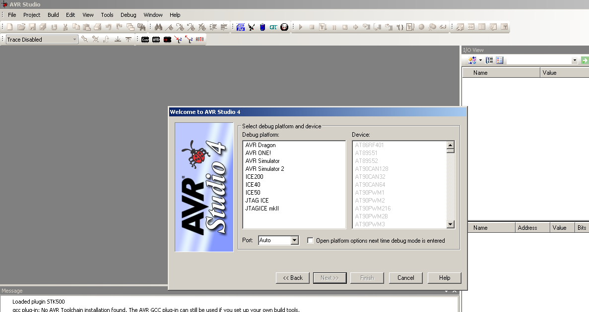
Hallo Forengemeinde, kann der AVR-ISP MKII einen AT89S52 auslesen? Es geht mir nur darum, den Inhalt zu 'sichern', und im Bedarfsfall diesen zu ersetzen. Das Datasheet zum AT89S52 gibt ja her, dass dieser eine ISP-Schnittstelle hat. Mein AVR-Studio
Thomas S. schrieb im Beitrag #7787806: > kann der AVR-ISP MKII einen AT89S52 auslesen Note: The AT89 devices that are supported by AVRISP mkII has the opposite reset polarity. If the AVRISP mkII has been
Der Compiler fragt ja beim Anlegen eines Projektes nach dem entsprechenden Device. Bei mir ist das: AT89C51RC2. Mein eigentliches Anliegen war: Ich wollte wissen ob jemand die Funktion kennt und wenn ja ob die Funktion funktioniert oder ein Fehler vorliegt. Wenn jemand die Funktion kennt, hätte ich
major (loss of generation) disturbances in the Nordic power system. Yesterday, November 17th, at 15:25:51, Olkiluoto 3 had another turbine failure, tripping all 1600 MW of generation and causing the Nordic system frequency to drop to 49.59 Hz. The failure is expected to last several days. - On
die letzten Postings diesr Diskussion anzeigt. https://www.youtube.com/watch?v=3rw0NmKw7as#t=3m10s
channel-to-channel turn-on time. After the first GSCLK goes high, OUT0 LOD status is valid; tpd3 + tpd2 = 60 nS + 1 s = 1.06 s. OUT1 LOD status is valid; tpd3 + td + tpd2 = 60 ns + 30 ns + 1 s = 1.09 s. OUT2 LOD status is valid; tpd3 + 2*td + tpd2 = 1.12 s, and so on. It takes 1.51 s maximum (tpd3 + 15*td + tpd2
the rate at which hi-cut 0x0014 Si4704/05-D50 and later, RELEASE_RATE increases the cut-off fre- Si4706-D50, quency. Default value is 20. Si4730/31/34/35-D60 and (approximately 3.3 s) later, Si4732 0x1A04 FM_HICUT
voltage and thus ensuring that the output current is clamped at the design value. Subject only to Q1’s ability to withstand the resulting power dissipation, the circuit can withstand either a brief or indefinite short circuit. AP1084 Vin Vin VR1 Vout V out GND
Daniel S. schrieb im Beitrag #7767921: > Moin, > > Ich bräuchte mal Hilfe mit einem Code für die Ansteuerung. > > Ich habe 11 Stück 74HC595, die jeweils 84 LEDs ansteuern, 4 Ausgänge > sind leer, die
wann aus Komfort- oder Geschwindigkeitsgründen das genaue Gegenteil angewandt werden darf – bei einem AT89C2051 oder AT89C51 kommt es auf jedes Byte an und dort muss man teilweise extrem sparen und oft auch zu Assembler greifen, weil auch der Flash relativ kurz ist, beim STM32 ist es Unsinn, krampfhaft
activated by software command OM changes are synchronized with the edges of UC1698u (that’s Software Reset) or by connecting RST pin to ground internal clock. To ensure consistent system states, wait at (that’s Pin Reset). command. S after Set Display Enable or System Reset In the following
. Max. Units Conditions I Continuous Source Current MOSFETsymbol D S -74 (Body Diode) A showing the I Pulsed Source Current integral reverse G SM -260 (Body Diode) p-n junction diode. S V Diode Forward Voltage -1.6 V T = 25°C, I = -38A, V = 0V SD J S GS trr Reverse Recovery
EFUSE_RD_RS_ERR0_REG (0x01C0) M NM L _N FA M ER_ NU NU NU NM FA NM _A ER M_ _U M_ FI R_ FI ER_ A ER FA R_ AT_ ER RT AT_ PI R1 PI8 Y3 Y_ Y2 Y3 Y_ Y2 Y_ Y1 RD Y_ S_A RD C_ S_P CS _E _K _KE _E _K _E _K _KE _S _K _Y _U _A _Y vd) _A US USE UE US UE US USE UE US UE US USE UE US sr US E EF E EF E EF EF E EF E EF EF
respective contributors. They do not constitute TI specifications and do not necessarily reflect TI's views; see TI's Terms of Use. TI E2E™ Online Community TI's Engineer-to-Engineer (E2E) Community. Created to foster collaboration among engineers. At e2e.ti.com, you can ask questions, share knowledge
Enabling ICache and DCache also is fundamental. Turning off ICache slows the 8bit read to 13.40 MB/s. Turning off DCache slows both 8 and 16 bit reads to 23.05 MB/s and 15.01 MB/s. 3. Configuring MPU on 0x8000000 seems to have no substantial effect at all if I\DCache are disabled. 4. Configuring
on SDRAM seems to have an important effect, but, enabling the bufferability seems to have no effect at all. Enabling the shareability when DCache is disabled get slow reading speeds: both 22.47 MB/s. My actual problem is, since I use SDRAM to store "slow" data (10Sa/s ADC) which have to be used for
is arailable in nals or will deliver 20 mA output current with 0.4V the limited temperature ranges at a cost savings. a tion. Reference output can be as low as 200 mV. n The circuit is recommended for portable equipment anFeatures d completely specified for operation from a single power cell. V In contrast
nur noch unter DOSBox laufen. Man braucht auch kein großes Entwicklungsboard mehr, ein AT89C51RB2 hat alles onboard. Mit Flip lädt man ein Programm über die UART in dessen Flash. https://www.digikey.de/de/products/detail/microchip-technology/AT89C51RB2-3CSUM/1245778 Die MCS51 lassen sich
NMOS waren. Noch zu DDR-Zeiten gab es CMOS-SRAM (U6516) im Bastlerladen. Damit habe ich dann später AT89C51 erweitert. Der 6516 hatte das nötige Adreßlatch ja schon eingebaut.

 Bild
Bild
 Bild
Bild