2019: 51%). • Befürchtungen über Störungen des Flughafenbetriebs nehmen allmählich ab (2025: 64%, 2022: 69%, 2019: 72%). • Die allgemeine Störung der Privatsphäre bleibt gleichbleibend bei rund 82% (2022: 79%, 2019: 83%). • Gefahren durch Unfälle wie Abstürze nehmen deutlich ab (2025
darüber, dass IAR vom Cross-Plattform-Spezialisten QT übernommen wird: [c] The cash deal, which at SEK180 is a 66% premium on the current share price. has the backing of the main institutional investors with 38% of the shares. Completion of the deal is conditional on 90% of the shareholders selling
the routine after a programmed start time so that you can reprogram the start time. Display 91 TAKE FIRST SAMPLE AT HH:MM DD-MMM This display appears when you have selected “YES” in Display #90. Enter the start time and date for the flow -pulse countdown.
512, and 768 fS. The TAS5558 accepts a 64-fS bit clock. The external crystal used must be 12.288 MHz. The TAS5558 also features power-supply-volume-control (PSVC), which improves dynamic range at lower power level and can be used as part of
ubuntu-release-upgrader should stop upgrades beyond Ubuntu 24.04 on hardware that does not support the RVA23U64 profile. RVA23U64 [1] is the profile relevant for user space. As there is no upgrade path from Ubuntu 25.04 Plucky for RVA20 systems, we should also stop upgrading these RISC-V systems from Noble
particular our first multicore support! Initially available on the RP2040 microcontrollers, now TinyGo can use both cores at the same time for true concurrency in hardware. Another very powerful new capability added in this release is USB Mass Storage Device (MSD) support on the RP2040/RP2350, SAMD21, and
Hallo, ich möchte einen AT90CAN128 über die serielle Schnittstelle programmieren. Dafür suche ich einen geeigneten Bootloader. Im Internet habe ich "ATmegaBOOT_168_at90can.hex" und "AVR-CAN_UART.hex" gefunden und mit einem
Nachtrag Ich habe eine Olimex AVR-CAN-Platine. Wenn ich das Blink-Programm mit dem AVR-Prog herunterlade, erhalte ich folgendes: avrdude -F -V -c avrispmkII -p c128 -P usb -U flash:w:0_blink_can128.hex:i avrdude: AVR device initialized
Die zwei Adressen wurden auch hier beobachtet: https://docs.buspirate.com/docs/devices/at24c256/ " This AT24C256 EEPROM is a non-original variant and includes an additional address: 0x58 (0xB0/B1). This extra address can be utilized to store data, such as a serial number. While this feature
nicht aufgibst. Vielleicht schaust Du dir mal diese Arduino lib an: https://docs.arduino.cc/libraries/at24c/ Die kümmert sich um I2C transfer buffer limit 32 byte AT24 page size 64 byte Aufruf mit beliebigem bytecount byc, z.B. beginned ab buffer[4] nach EEPROM adr: [c] const uint8_t bufSiz =
● CPU load and task execution graphs ● Support for custom tracepoints Developers can use View for free, and registration unlocks additional features at no cost. [/c] ### ic-Haus iC-LFMB - neuer Linien-CCD ic-Haus ist einer der wenigen „rein deutschen“ Halbleiter-Hersteller: Das
process without compromising measurement accuracy. Technical Highlights iC-LFMB is a 64-pixel linear image sensor with a special pixel geometry. The sensor contains 64 active photo pixels measuring 56 µm × 600 µm each. The pixel pitch of 63.5 µm corresponds to a resolution of 400 DPI.
architecture — Pinout and software compatible with single-power-supply Flash standard — 8 uniform sectors of 64 Kbytes each — Any combination of sectors can be erased — Superior inadvertent write protection — Supports full chip erase Data# Polling and toggle bits — Sector protection: — Provides a software method
the GDB manual and other documentation resources online at:\n <" -> ~"http://www.gnu.org/software/gdb/documentation/>.\n\n" -> ~"For help, type \"help\".\n" -> ~"Type \"apropos word\" to search for commands related to \"word\".\n" -> 1^done 2-gdb-set
http://openocd.org/doc/doxygen/bugs.html CDLiveWatchSetup embedded:startup.tcl:28: Error: Can't find raspberrypi-swd.cfg in procedure 'script' at file "embedded:startup.tcl", line 28 [/code]
active at 1. In interrupt trigger mode, when THR empty interrupt from UART is received, if FIFO is enabled, up to 8 bytes can be written to THR and FIFO at a time, and then will be transmitted automatically by
near−unity power at the most stressful conditions while DCM limits the factor while operating in any type of Discontinuous switching frequency at lower load. The circuit can also Conduction Mode operation: DCM or CRM. transition
supply voltage rises above the UVP threshold level, the system restarts. The UVP threshold is set at 6 V minimum supply by default but can be changed to 8 V minimum supply using bit IB4[D7]. OverVoltage Protection (OVP) is activated when the supply voltage exceeds the OVP threshold. The OVP (or load
92 92 V/s 10 uF 8.8 9.6 10.4 V/s 9.3.2 Active Current Limiting (ILM) The load current is monitored at all times. When the load current exceed the current limit trip point ILM programmed by RILM resistor, the device regulates the current within t . The following equations can be used ILM to find the RILM
3D-Ansicht von hier: https://www.phoenixcontact.com/de-de/produkte/kontakteinsatz-sacc-ci-m12fsdr-4con-l90-thr-r-1028581)
>Our new decorative paints system acts like a sunscreen. The surface >temperature of buildings can be lowered by up to 10%. Wow, statt 300 K ist meine Hauswand dann nur noch 270 K warm? Nett!
dBm (RFO_HP) • low output power, programmable up to +15 dBm (RFO_LP) In an application, the customer can choose to use an RF output (RFO) or both RFOs, using a DC switch for biasing circuit. Note: Only one RFO can be used at a time. When using one RFO, only one RF Tx matching circuit is necessary as shown
may cause permanent damage to the device. This is a stress only rating and operation of the device at these or any other conditions above those indicated in the operational sections of this specification is not implied. o Electrical Specifications V DD- VSS= 3.0V, OSC= 4.194304MHz, Test Circuit,AT = 25
100 100 100 90 90 90 80 80 80 P o 70 70 70 w 60 60 60 50 50 50 e 40 40 40 r 30 30 30 I n 20 20 20 l 10 10 10 e 0 0.1 1 10 30 0 0.1 1 10 30 0 0.1 1 10 30 t Frequency in MHz Frequency in MHz Frequency in MHz F i l e L Models r s 6A 10A & db db 100 100 P 90 90 o 80 80 w 70 70 60 60 e r 50 50 E 40 40 n 30 30 20 20 r 10 10 y 00.01 0.1 1 10 30 00.01 0.1 1 10 30 M Frequency in MHz Frequency in MHz o d Z Models u l e s 6A 10A db db 100 100 90 90 80 80 70 70
SDRAM) dual inline memory modules (DIMMs). The memory sockets on the system board are populated with at least one preinstalled memory module. To achieve the maximum memory support, you can populate the system board with up to 64 GB of memory configured in a high-performing dual-channel mode. For proper
Zusätzlich muß die Interrupttabelle angepaßt werden auf den "neuen" µC. beispielsweise sieht diese beim At13 so aus: If the program never enables an interrupt source, the Interrupt Vectors are not used, and regular program code can be placed at these locations. The most typical and general program setup
the T-bit as source and destination for the operated bit. A bit from a register in the Register File can be cop- ied into T by the BST instruction, and a bit in T can be copied into a bit in a register in the Register File by the BLD instruction. 16 AT90S2313 0839I–AVR–06/02 AT90S2313 Bit 5 – H: Half-carry
this, select the and total runtime of the „Overheated Alarm battery. Switch“ fjeld. • - Settings You can illuminate You will fjnd the at the battery’s charge the top right after you level indicator using have selected the bat- the „Battery identifj- tery. 48 GB MT Press the icon again The battery can also
For UTC LM7809 (V =1IN) PARAMETER SYMBOL TEST CONDITIONS MIN TYP MAX UNIT TJ=25°C, IOUT=5mA - 1.0A 8.64 9.0 9.36 V Output Voltage V OUT VIN=11.5V ~ 24V, 8.55 9.45 V IOUT=5mA - 1.0A,PD≦15W Dropout Voltage V D TJ=25°C 2.0 V TJ=25°C,I OUT=5mA - 1.0A 90 mV Load Regulation ΔVOUT TJ =25°C,IOUT=0.25A - 0.75A 45 mV VIN11.5V ~ 25 V, T J25°C 90 mV Line regulation ΔVOUT VIN=11.5V ~ 24V, T J25°C, I OUT=1.0A 90 mV Quiescent Current Q TJ=25°C, IOUT≦1.0A 8.0 mA Quiescent Current Change ΔI VIN11.5V ~ 24V 1.0 mA Q IOUT=5mA – 1.0A 0.5 mA Output Noise
circuit either not working or “playing up” on too low a current range – that’s the burden voltage at work, starving your circuit of the voltage it needs to function correctly. You usually have no option but to reluctantly switch to a higher current range to lessen the effect. The problem can also be
Battery Before using this feature, the UPS must have been powered by utility power with output enabled at least once. Battery start can be disabled. See the "Cold start" setting in "ON/OFF Settings" on page 11. To start the UPS on battery: 1. Press the button on the UPS front panel until the UPS front panel
pneumatic power unit together with product specific “quick change” tooling packs. The insertion heads can be equipped with a rotary insertion finger that can apply products at different angles without decreasing the insertion rate. The tooling packs can be exchanged within 30 minutes to meet your full range
built-in DC/DC converter.) (6) Normal / Extended temperature type. (7) Excellent LC : VOP maintains at 5V for whole temp. range, no need extra temp. compensation circuit. 2 NUMBERING SYSTEM AC-202A _ _ _ _ - _ 1 2 3 4 5 No Code Value Description Remark 1 G STN gray type LCD LCD Type Y STN yellow green
IO-Link remains stable and has been growing continually for years, with more than 61 million nodes at last count. IO-Link continues to successfully establish itself as a global standard. PROFIsafe This kind of trend can also be seen with PROFIsafe nodes. Following exceptional growth in the preceding
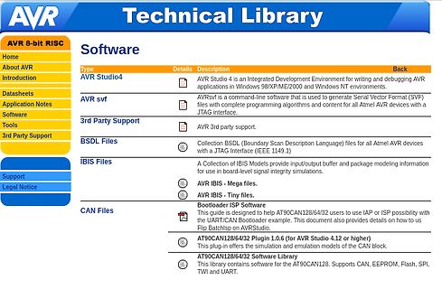
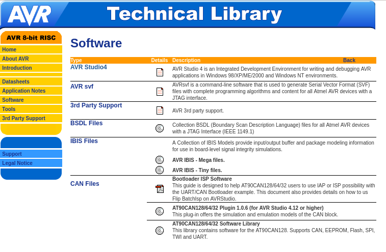
3rd Party Support
Support
Legal Notice
AVR Studio4
AVR svf
3rd Party Support
BSDL Files
iBIS Files
CAN Files
AVR 3rd party support.
Collection BSDL files for all Atmel AVR devices with a JTAG interface (IEEE 1149.1)
A Collection of IBIS Models
AVR IBIS - Mega files.
AVR IBIS - Tiny files.
Bootloader ISP Software
AT90CAN128/64/32 Software Library
modes, to keep track of time. It can wake up the device from sleep modes and/or interrupt the device at regular intervals. The reference clock is typically the 32.768 kHz output from an external crystal. The RTC can also be clocked from
Hallo, ich bin auf der Suche nach einer Fassung für den AT90CAN128. So, wie die hier https://www.reichelt.de/de/de/shop/produkt/ic-fassung_68-polig_plcc-14703 Allerdings in 64-polig. Bei meiner Suche finde ich nur 68-polig. Weiss jemand, wo ich die
Andreas schrieb im Beitrag #7859038: > ich bin auf der Suche nach einer Fassung für den AT90CAN128. Es gibt Nullkraft-Fassungen zum Programmieren der Controller, z.B. diese hier: https://eckstein-shop.de/Enplas-OTQ-64-08-01-IC-Test-Burn-in-Socket-for-QFP64-TQFP64-FQFP64-PQFP64-package
CARD_POWER 1 G N D 20 FG1 DIR G LOW = Power OFF FG2 TC74VHCT245AFT SCAB1A8100 R255 1 IC94B 100k HD74LV32AT D IC90C IC90D RPC05T@J D 5 CARD_XBUSEN HD74LV00AT HD74LV00AT XCARD_BUS_ENABLE 6 RPC05T@J 9 12 XCA_IOIS16 4 R254 22 8 11 XIOIS16 10 13 RPC05T@J R256 NIU D +5 D +3.3 D LTLXBIG LTLXBIG R257 0 R258 NIU R259
the forward converter works at the pre-regulated intermediate circuit voltage. This means that a higher transformer ratio can be selected, reducing the current load for the MOSFET. Furthermore, a larger duty cycle can be set during
CARD_POWER G N D FG1 1 DIR G LOW = Power OFF 20 FG2 0 TC74VHCT245AFT SCAB1A8100 R255 1 IC94B 100k HD74LV32AT D IC90C IC90D RPC05T@J D 5 CARD_XBUSEN HD74LV00AT HD74LV00AT XCARD_BUS_ENABLE 6 RPC05T@J 9 12 XCA_IOIS16 4 R254 22 8 11 XIOIS16 10 13 RPC05T@J R256 NIU D +5 D +3.3 D LTLXBIG LTLXBIG R257 0 R258 NIU R259
addition, there is a user range. User write to the memory is restricted to the NVM User Range. User read can also be performed to the other NVM addresses. 4.8.1 NVM User Range The host can write and read the memory of the user range. The range is located at addresses 0x20-0x22. Each address holds 2 bytes.
is enabled with ACC_CONF.acc_perf_mode=0b1. In this power mode, the accelerometer data is sampled at equidistant points in the time, defined by the accelerometer output data rate parameter ACC_CONF.acc_odr. The output data rate can be configured in one of eight different valid ODR configurations going
This pin is Data/Command control pin connecting to the MCU. When the pin is pulled HIGH, the data at D[7:0] will be interpreted as data. When the pin is pulled LOW, the data at D[7:0] will be transferred to a command 12 D/C register. In I2C mode, this pin acts as SA0 for slave address selection. When
high- current drive capability for directly driving LEDs. Each 2 Applications quasi-bidirectional I/O can be used as an input or output without the use of a data-direction control • Telecom Shelters: Filter Units signal. At power on, the I/Os are high. In this mode, • Servers only a current source to V
6 7 8 9 1 2 3 SDA Data from transmitre Data from transmitre Transmitter must release the SDA line at this point, Receiver must release the SDA line allowing the Receiver to pull the SDA line low to at this point so the Transmitter can acknowledge the previous eight bits of data. continue sending data

 Bild
Bild