The data bus is in a high-impedance state when either CE# or 3.4 Chip Erase Operation OE# is high. Refer to the Read cycle timing diagram (Figure 7-1) for further details. The SST39LF010/020/040 and SST39VF010/020/040 devices provide Chip Erase operation, which allows the user to erase the entire memory
WFS VD=V DB5V, V =5IN - - 0.55 V Short circuit trip level V = 15V (Note 4) 0.455 0.480 0.505 V SC(ref) D UV DBt Control supply under-voltage Trip level 10.0 - 12.0 V protection(UV) for P-side of UV DBr inverter part Reset level 10.5 - 12.5 V UV Dt Control supply under-voltage Trip level 10.3 - 12.5
HORD[10:8] – Horizontal Starting Position (Upper bits) of Character displaying. These bits with Cfg_02h, total 11 bits, become 2048 steps, with an increment one pixel per step. 2.10.4.3 Cfg_02h – Character Delay_2 (Default=10h) Table 2-7 Cfg_02h – Character Delay_2 7 6 5 4 3 2 1 0 HORD[7] HORD[6] HORD
August 2016 4 of 31 NXP Semiconductors PCA9532 16-bit I C-bus LED dimmer 6. Functional description Refer to Figure 1 “Block diagram of PCA9532”. 6.1 Device address Following a START condition, the bus master must output the address of the slave it is accessing. The address of the PCA9532 is shown in Figure
information on these power options and how to Strainer /4" Vinyl 8" Vinyl 8 " Teflon maintain them, refer to the Power Products Guide Line Line Line that was shipped with your sampler. StainlessSteel ------- 22 feet 15 feet Placement of the Sampler Low-Flow 14 feet 7 feet ------- StainlessSteel Refer to
specifications are subject to change without prior notice. 2. As for spare parts order and supply, refer to the "GUIDEBOOK for Spare parts Supply", pub- lished seperately. 3. The numbers in item column correspond to the same numbers in drawing. – 23 – 1 PX-720_BLACK_DI_120V 6 PX-720_CHERRY_DI_120V 2 PX
0.3 0.2 F VCE(sat) IC B = 10 h 0.1 0.2 0 0.2 0.5 1.0 2.0 5.0 10 20 50 100 200 0.1 0.2 0.3 0.5 0.7 1.02.0 3.0 5.0 7.0 10 20 30 50 70 100 C , COLLECTOR CURRENT (mAdc) C , COLLECTOR CURRENT (mAdc) Figure 1. Normalized DC Current Gain Figure 2. “Saturation” and “On” Voltages 2.0 1.0 V C E TA= 25°C / -55°C
REVISED APRIL 2015 www.ti.com MUTE Normal Normal VOLUME Operation Operation t t d(VOL) d(VOL) T0032-02 Figure 6. Mute Timing HP_SEL tw(HP_SEL) Spkr Volume td(VOL) td(VOL) td(VOL) HP Volume t(SW) t(SW) t d(VOL) T0033-02 Figure 7. HP_SEL Timing SCLK (Input) t h1 tsu1 LRCLK (Input) t h2 t su2 SDIN1 SDIN2
stehen ja 16 Bytes. Wieso geht die Adresse nur 10 > Bytes weiter? Hexadezimal. [pre] 00 01 02 03 04 05 06 07 08 09 0A 0B 0C 0D 0E 0F 10 11 12 13 14 15 16 17 18 19 1A 1B 1C 1D 1E 1F [/pre]
hat der Editor wohl doch recht :D Daniel A. schrieb im Beitrag #7891552: > Hexadezimal. > 00 01 02 03 04 05 06 07 08 09 0A 0B 0C 0D 0E 0F > 10 11 12 13 14 15 16 17 18 19 1A 1B 1C 1D 1E 1F Die Adressen sind ja auch in HEX -> 10 Hex = 16 Dec Danke für die Denkanstöße
command to re-en- the device code. A read cycle containing a sector ad- dress (SA) and the address 02h in returns 01h if that able the device for reading array data if DQ5 goes high, sector is protected, or 00h if it is unprotected. Refer to or while in the autoselect mode. See the “Reset Com- the Sector
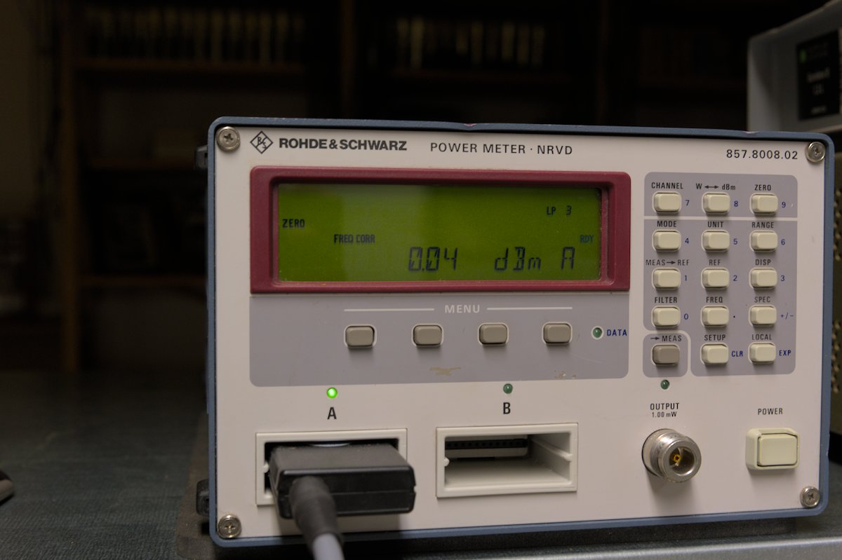
ROHDE & SCHWARZ POWER METER NRVD 857.8008.02 ZERO LP 3 FREQ CORR RDY 0.04 dBm A CHANNEL MODE UNIT RANGE MEAS REF REF DISP FILTER FREQ SPEC DATA MEAS SETUP LOCAL CLR EXP OUTPUT 1.00 mW POWER
SZP6SMBxxxAT3G SMB 2,500 / (Pb−Free) Tape & Reel †For information on tape and reel specifications, refer to our Tape and Reel Packaging Specifications *Please see P6SMB11CAT3 to P6SMB91CAT3 for Bidirectional devices. Brochure, BRD8011/D. **For additional information on our Pb−Free strategy and soldering
For information on tape and reel specifications, including part orientation and tape sizes, please refer to our Tape and Reel Packaging Specifications Brochure, BRD8011/D. *Bidirectional devices will not be available in this se- ries. **The “T3” suffix refers to a 13 inch reel. Individual devices are
einzubauen wegen der RS485 Schnittstelle. schnittstellehttps://epa.de/download/de/04_Betriebsanleitungen/04.02_Antriebe/04.02.01_Frequenzumrichter/04.02.01.07_LSIS/LSIS_iG5A_Betriebsanleitung.pdf
der RS485 > Schnittstelle. > schnittstellehttps://epa.de/download/de/04_Betriebsanleitungen/04.02_Antriebe/04.02.01_Frequenzumrichter/04.02.01.07_LSIS/LSIS_iG5A_Betriebsanleitung.pdf Danke dafür
For information on tape and reel specifications, including part orientation and tape sizes, please refer to our Tape and Reel Packaging Specifications Brochure, BRD8011/D. http://onsemi.com 8 MC1489, MC1489A MARKING DIAGRAMS SOIC−14 D SUFFIX PDIP−14 P SUFFIX CASE 751A CASE 646 14 14 14 14 MC1489ADG MC1489DG
with1.0 k -1.0 - V CC V V SAT Output VSAT IO= 10 mA – 0.10 0.40 V ISING Output Leakage V O 7.0 V – 0.02 10 A V CC-TH Low V CCDisable Threshold 7.0 8.0 8.5 V V L Logic 0 Input Voltage 1.0 1.6 – V Voltage Regulator Section V REF Output Voltage 6.25 7.00 7.50 V IO Output Load Current - - 10 mA V REF-LOAD
is still in effect. [19:0] Reserved RO Reserved 0 For the operation or setting of FlashROM, please refer to related subprograms. This datasheet does not provide the introductions to FlashROM word data registers and FlashROM control registers. 4.4 Flash-ROM Operation Steps 1. Erase Flash-ROM, please refer to and call related subprograms. 2. Write Flash-ROM, please refer to and call the related subprograms. 3. Read DataFlash, please refer to and call related subroutines. 4. Read CodeFlash, through a pointer to the program storage space. 4.5 Unique ID Each chip has
i input voltage - 2.45 - V SVRR voltage and ACGND input bias voltage in Mute and Operating modes V ref reference voltage input ACGND pin - 2.45 - V half supply reference SVRR pin - 7.2 - V Amplifier outputs; pins OUT1N, OUT1P, OUT2N, OUT2P, OUT3N, OUT3P, OUT4N and OUT4P V O(offset) output offset voltage
literature number SLUA271 (www.ti.com/lit/slua271). 5. Vias are optional depending on application, refer to device data sheet. If any vias are implemented, refer to their locations shown on this view. It is recommended that vias under paste be filled, plugged or tented. www.ti.com EXAMPLE STENCIL DESIGN
part has multiple moisture sensitivity ratings, only the lowest level per JEDEC standards is shown. Refer to the shipping label for the actual reflow temperature that will be used to mount the part to the printed circuit board. (6) Part marking: There may be an additional marking, which relates to the
description. Das kann man ja mal prüfen! https://www.ti.com/lit/ug/spru018d/spru018d.pdf?ts=1748181432238&ref_url=https%253A%252F%252Fwww.google.com%252F Wobei es da wohl keinen Disassembler gibt. Danke vielmals für diese neue Idee. EDIT: also dass es Register A0..A5 und R0..3 gäbe konnte ich noch
0x00 0x01 +14 +10 0x01 +13 +22 0x04 0x07 High power +20 0x03 0x05 +22 (RFO_HP) 0x00 0x01 +17 0x03 0x02 +14 0x02 +14 AN5457 - Rev 3 page 19/75 AN5457 Power amplifier network Caution: To avoid exceeding the maximum ratings that may cause irreversible damage to the device, some restrictions must be followed
the @ref Sn_IR(0) becomes * But when a TCP clientconnection request is failed, @ref Sn_IR(3) becomes and the status of @ref Sn_SR changes to SOCK_CLOSED. */ #define Sn_CR_LISTEN 0x02 /* @brief Send connection
steel plate St 12, minus the weight of the reading head itself. 62056-21 IEC:2002 – 27 – IEC 728/02 Cohesion force F ≥5 N in contact with the steel plate; F > 1.5 N at a distance of 2 mm from the steel plate. Figure 3a – Cohesion force IEC 729/02 Internal diameter d = 13 mm ± 1 mm; External diameter
that is, the number of Si is 1. For the specific value analysis of the distance and angle, please refer to the following; When CT[bit(0)]=0 is detected, it indicates that the packet data is a point cloud data packet; Zur Qualität steht da nichts drin, aber der Code ist ja auch für ein anderes Lidar
Flash (Continued) DATA DATA HIGH XA1 XA0 BS XTAL1 WR RDY/BSY RESET +12V OE 64 AT90S2313 0839I–AVR–06/02 AT90S2313 Reading the Flash The algorithm for reading the Flash memory is as follows (refer to “Programming the Flash” for details on command and address loading): 1. A: Load Command “0000 0010”. 2.
Crimping Applicator machine Applicator Crimp applicator with dies SACH-003G-P0.2 MKS-L-10-3 APLMK SACH003-02 AP-K2N SACH-003G-P0.2B MKS-L-10-3 APLMK SACH003-02 Note: Contact JST for fully automatic crimping applicator. - 1 - ACH CONNECTOR Housing No. of circuits Model No. Dimensions(mm) Q'ty/ <Single circuit> <2, 3 circuits> A B bag Mark of No.1 circuit 1 ACHR-01V-A-S - 1.6 2,000 2 ACHR-02V-S 1.2 2.6 1,000 3 ACHR-03V-S 2.4 3.8 1,000 P ACH CONNECTOR U 4 ACHR-04V-A-S 3.6 5.0 1,000 B B A S 5 ACHR-05V-A-S 4.8 6.2 1,000 1 3 H 3.5 Material and Finish Thermoplastic resin, UL94V-0, natural (white
Time T 150 250 400 μs SIP CONTROL OUTPUT VOLTAGE(OD&OC) OD Pin Output “H” Voltage V DH VDD-0.1 VDD-0.02 V OD Pin Output “L” Voltage V DL 0.2 0.5 V OC Pin Output “H” Voltage V CH VDD-0.1 VDD-0.02 V OC Pin Output “L” Voltage V 0.2 0.5 V CL 0V BATTERY CHARGE FUNCTION Charger start Available 0V voltage(available
Funktionsgeneratoren mit 12 Bit DA-Wandler. Diese haben beide einen ( gemessenen ) Klirrfaktor von 0,02% bei Frequenzen kleiner als 100KHz. Ralph Berres
Klirrfaktormessbrücken Unsere Messkisten hatten eine Referenz Funktion. Zuerst wurde der Messsender gemessen, REF gedrückt, dann die Übertragungsstrecke gemessen. Der dann abgelesene Wert entsprach der eher der Realität.
www.amazon.de/AILOOCEDI-BNC-Buchse-Adapter-BNC-Buchse-50KY-Q9-Adapter-Anschlusszubeh%C3%B6r/dp/B0D1GH9WMB/ref=sr_1_3? und baut einen Messwiderstand nach eigener Vorstellung ein.
hier rumliegen weil ich mal damit spielen wollte, aber man kommt ja zu nix.... Weitere Teile: MCP6C02 (500khz), TSC1801(2Mhz), ISL28006(100-180khz), NCS7030(100khz), AD8412A(1,8Mhz), MPQ8113(700khz) Und oh, was muss ich da erblicken: MAX49918 Bandbreite von 25 bis 75khz, aber acht verschiedene Verstaerkerstufen
Ion INR18650 MJ1 3500mAh 2016-06-30 1 Revision History Revision Date Originator Description 0 2016-02-19 Lee, Kwanhee - Draft - Some items of “5. Caution and prohibition in 1 2016-06-30 Lee, Kwan hee handling” were added. 2/10 PRODUCT SPECIFICATION CONFIDENTIAL Description Date Rev Lithium Ion INR18650
) Value might change after device evaluation has finished. Notes 1. n: Number of macro instances. Refer to the User Manual for the detailed specification. 2. m: Number of channels. Refer to the User Manual for the detailed specification. Notes 1. n: Number of macro instances. Refer to the User Manual
0.58 0.85 0.94 1.11 1.36 1.61 1.87 2.12 2.36 2.50 2.68 3.05 Liquid temperature no subcooling 32°C refer to 101N2100 Instructions for details specifjcations FRCC.PK.047.A2.02 - Manufactured by Secop for Danfoss 77 Hermetic Compressors for DC Voltage BD1.4F-VSD Direct Current Compressor R134a, 12-24V DC
nicht. Fakt ist: Zwischen 12V und Masse darf es keine 0.5 Ohm oder ähnlich geben. Ob es nun 0.02 oder 0.7 Ohm sind, ist völlig egal. Beides ist nicht korrekt. Lothar
bekanntlich mit der Frequenz. https://www.ti.com/lit/ds/symlink/csd95495qvm.pdf?ts=1745776746748&ref_url=https%253A%252F%252Fwww.mouser.de%252F
CP2110-F01-GM (QFN24, 4 x 4 mm, Pb-free) Supports Windows 7, Vista, XP, Server 2003, 2000 CP2110-F02-GM1 (QFN28, 5 x 5 mm, Pb-free) Supports Mac OS X - QFN28 is pin-compatible with the CP2102-GM. Supply Voltage Temperature Range: –40 to +85 °C Self-powered: 3.0 to 3.6 V USB bus powered: 4.0 to
R206 R2I0 R25 5 TT TT2 flc I YT_AC Y1_DC YTZTOÜÜFF YTITODON YTJTOÜFF YT:TooTT “ZV RZZGT C a L \. 1 T ı02oT2A Tc2012B To oFFs_T R22 5'< U c2T42 R22e0 C ae 3CK043 B C2029 9 R2055 .02 JJR2 C02u. CR22s2 nox U _5v C RZOEB Z2 -ev +T2\/ DC RZUG4 56T?2 QNOOON TR DC OOOÜNOOOOOFF RzoTT R2n4s 0 B 2'O~.< 2:ww--<† T
Junction-ambient max. 85 13 (*) 60 35 (*) Mounted on aluminium substrate. ELECTRICAL CHARACTERISTICS (Refer to the Test Circuits; T = 25⋅C, V = j2V, V S sens= 0, unless otherwise specified). Symbol Parameter Test Conditions Min. Typ. Max. Unit V s Supply Voltage 12 36 48 V Vref Reference Voltage REF = 2mA
CP2110-F01-GM (QFN24, 4 x 4 mm, Pb-free) Supports Windows 7, Vista, XP, Server 2003, 2000 CP2110-F02-GM1 (QFN28, 5 x 5 mm, Pb-free) Supports Mac OS X - QFN28 is pin-compatible with the CP2102-GM. Supply Voltage Temperature Range: –40 to +85 °C Self-powered: 3.0 to 3.6 V USB bus powered: 4.0 to
Hole External Shaft Shaft Length (with tachometer)iameter Length Spacing Dimension Diameter Length (Ref) (Ref) (Ref) (Ref) (Ref) DPP240 4.0 in 6.1 in 0.2500 in 0.2495 in [4] 6-32 UNC-2B DPP242 5.0 in 7.1 in 1.00 in 1.000 in 0.10 in 0.38 in Deep Min 1.083 in 2.00 in 0.2497 in 0.70 in 0.74 in ±0.03 0.998

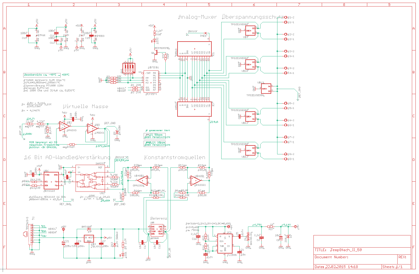
 Bild
Bild
 Bild
Bild
 Bild
Bild