Hysteresis 100 mV Current (Shutdown) V EN0V 0.1 1 µA Quiescent Current (PFM) V FB0.7V,No switch 100 200 µA Quiescent Current (PWM) V FB.5V,switch 1.6 2.2 mA Switching Frequency 1.2 MHz Maximum Duty Cycle V FB0V 90 % EN Input High Voltage 1.5 V EN Input Low Voltage 0.4 V FB Voltage 0.588 0.6 0.612 V FB
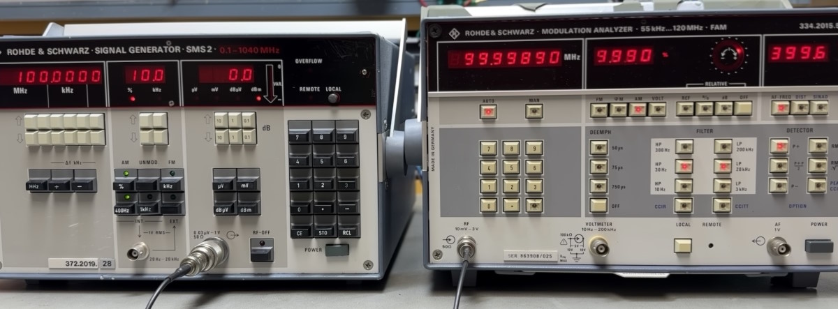
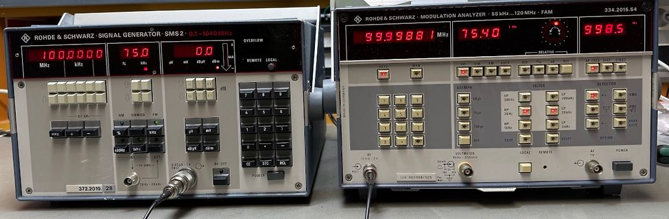
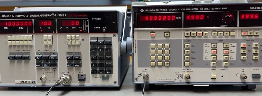
MODULATION ANALYZER 55...120 MHz FAM 334.2018.3
99.99890 MHz 9.990. 399.6
RELATIVE
AUTO MAN FM AM VOLT REF
HP 300 Hz 50 ps
LP 200 kHz
HP 30 Hz 75 ps
LP 20 kHz
OFF 750 ps
LP 3 kHz
10 Hz
CCIT
VOLTMETER 10mV-3V
LOCAL REMOTE AF
60Ω 10kHz-200kHz
POWER
achten, damit das Voltmeter von dieser verschont bleibt. Zu präziser Sub-Ohm-Messung: Hier ein MR200 von http://www.schuetz-messtechnik-gmbh.de/ , das Sub-mikro-Ohm auflösen kann: https://www.mikrocontroller.net/topic/400011#new Es gibt auch ein MR300.
Stromkreis. Du übertreibst. Bei einem Strom von 1A und einem typischen 3 1/2 Digit Multimeter im 200mV Bereich kannst du 1 mΩ gut messen.
SMD-Marking "N1IF": https://www.amazon.de/2PCS-Boost-Converter-Stromversorgung-Modul-Gr%C3%BCn/dp/B07NDF94DW/ref=pd_sbs_d_sccl_1_4/260-0147289-9328345 oder auch dieser: https://www.amazon.de/Konverter-Modul-DC3-15V-einstellbarer-Step-Down-Spannungsregler-Netzteilmodul/dp/B09T2LQFYS/ref=pd_sbs_d_sccl_1_2/260
gehen. Dabei fließt natürlich ständig Strom durch den Spannungsteiler und dem Chip-Port nach Masse (~200 µA). Besser wäre es vermutlich den Akku nur bei einer Messung zum Spannungsteiler/ADC zu führen? Z.B. mit einem kleinen Mosfet dessen Gate von einem IO-Pin gesteuert wird. IOs habe ich ja genug und
of the He spectrum used for the calibration. Note that the position of the indicated wavelengths (Ref. 7), given in nanometer, are not to scale. (b) Wavelength on the central pixel column of the CCD as function of the angular position a of the grating. (c) Horizontal pixel number p onto which a fixed
output latch function C: Without CO pin output latch function (CTL pin is pulled up internally) *1. Refer to the tape drawing. *2. Refer to “3. Product Name List”. (2) 8-Pin TSSOP S-8264 x xx - T8T1 x Environmental code U: Lead-free (Sn 100%), halogen-free G: Lead-free (for details, please contact our
Oszibild war ungenügend, jetzt besser. Die Spannung steigt bis 14V, dann geht es los. Übrigens jetzt mit 200V DC.
R323 parallel = 4,4k und den 680ohm als Vorwiderstand für den OK. Zusätzlich noch ein C parallel zu REF und C vom TL431. Das war es. Auf der Primärseite nur ein C parallel zu CE Strecke, E auf GND, C an den Schaltregler
impedance matrix is done by the following formula. [Z ] = G −1 · ([E] − [S])1 · [S ] · Z + Z ∗ · G (19.2) ref ref ref ref Converting a scattering parameter matrix to an admittance matrix can be achieved by computing the following formula. −1 [Y ] = G −1 · [S ] · Z + Z ∗ · ([] − [S]) · G (19.3) ref ref ref ref
tfmname ↔ fontfile mapping is the most prominent use of the pdftex.map file. The font file name must refer to a Type 1 or TrueType font file. If the fontfile field is missing, no font embedding can take place; a warning will be given, unless the psname field contain one of the 14 standard font names. Not
finde. Ich habe bei mir ein Mean Well Netzteil aus der UHP Serie verbaut, das gibts aber erst mit 200 W, also noch mehr Reserve ;) Florian schrieb im Beitrag #7961140: > Der LED-Streifen soll an Anfang, Mitte und > Ende parallel eingespeist werden, um den Spannungsabfall möglichst > gering zu
z.B.: https://www.amazon.de/Kompakter-Controller-Mikrofon-Adressierbarer-Streifen/dp/B0F2D4VBKF/ref=sr_1_3_sspa Florian schrieb im Beitrag #7961579: > Also, wenn ich richtig verstanden habe sollte ich wahrscheinlich eher > auf einen normalen RGBCCT Streifen mit 60 Leds/m wechseln. Welche Marke
Spannungsteiler und den ADC (PB3) aktiviert, einen dummy-ADC-Zyklus startet und die eff. Spannungen an ADC_REF (PB3) und PTC_IN (PB4) einliest. Die Ergebnisse ADC_max und ADC_werden anschliessend in der Funktion 'berechne_celsius()' per Tabelle ausgewertet und umgerechnet. Die Routine 'sende_werte()' erledigt
variable names are unique in their first two characters only. Thus, the variable names SA, SAM and SAMMY refer to the same storage location. LEGAL NAMES FOCAL RECOGNIZES KNOCK KN PROFIT PR COST1 CO (Thus COST1 and COST2 COST2 CO are the same!) ILLEGAL NAMES REASON 3ARM First character must be be alphabetic.
4.5 18 V Shutdown Supply Current ISD VRUN= 0V 0.1 1 uA VRUN= 2V, VFBK= Quiescent Current Q 105% V REF LOAD= 700 uA 0A UVLO Threshold V UVLO VPWR Rising 3.8 4.2 4.5 V UVLO Hysteresis V 300 mV UV-HYST Output Load Current I 2 A LOAD Reference Voltage V 4. 5V ≤ V ≤18V 0.749 0.765 0.781 V REF PWR Switching Frequency FSW 500 600 700 KHz Short Frequency FSHORT VOUT= 0V 200 KHz High Side MOSFET On-Resistance R DS(ON)-HM 120 mΩ Low Side MOSFET RDS(ON)-LM 100 mΩ On-Resistance High Side MOSFET ILIM-HM 2.5 4 A Current Limit High Side MOSFET I VRUN= 0V, VSWITCH 1 10 uA Leakage
device functionality should not be assumed, damage may occur and reliability may be affected. 2. Refer to ELECTRICAL CHARACTERISTICS, RECOMMENDED OPERATING RANGES and/or APPLICATION INFORMATION for Safe Operating parameters. 3. This surge voltage developed by the switching operation due to the wiring
Figure 5. VFversus IFfor Different Temperatures (VDD = 15 V) 1,400 1,400 VPN = 300 V VPN = 300 V )1,200 V = 15 V ) 1,200 V = 15 V m DD m DD ( s s1,000 s 1,000 L L g 800 g 800 i TJ= 100°C i c 600 c 600 i i S S TJ= 100°C , 400 ,F 400 O TJ= 25°C O TJ= 25°C E 200 E 200 0 0 0 5 10 15 20 25 30 0 5 10 15 20
gives an overview of the available devices in the Compact IPM series. For package drawing, please refer to Package Outline chapter. Table 1. DEVICE OVERVIEW NFAQ1060L33T Device STK5C4U332J−E NFAQ0560R43T NFAQ0860L36T NFAQ1060L36T NFAQ1560R43T(L) Feature triple shunts Package DIP−S DIP−S6 (Standard DIP
hoch ist die Nennspannung? > > 10V Und du hast eine ausreichend genaue Referenzspannung? z.B. REF5010-I oder -EI?
aber mit ihrer 1n329 als Referenz eher nur 5,5stellig genau. Dafür bekommt man diese meist für 150-200€. Um 200€lässt sich manchmal auch ein Prema5000 ergattern. Dieses ist 6,5stellig und hat meines Wissens eine LM399 als Referenz.
Kommt mir komisch vor, habs deswegen mit 3 Widerständen gemacht. Und nochmal im Leerlauf, auch ca. 200kOhm Ich hab jetzt den R13 bei 4,7k gelassen und unten den R15 auf 4,7k hoch. Wenn das mit den ca. 200kOhm stimmt dürfte es so gehen. Zumindest in der Simulation.
brauchen. Denn dann fließen 250mA über einen Versorgungs-Pin und dessen Bonddraht, der nur maximal 200mA aushält.
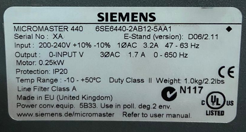
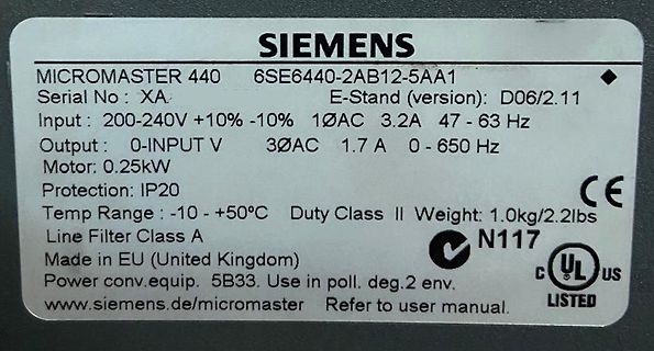
SIEMENS
MICROMASTER 440 6SE6440-2AB12-5AA1
Serial No : XA.
E-Stand (version): D06/2.11
Input : 200-240V +10% -10% 1ØAC 3.2A 47 - 63 Hz
Output : 0-INPUT V 3ØAC 1.7 A 0 - 650 Hz
Motor: 0.25kW
Protection: IP20
Temp Range : -10 - +50°C Duty Class II Weight: 1.0kg/2.2lbs
CE
N117
Made in EU (United Kingdom)
UL LISTED US
Power conv.equip. Use in poll. deg.2 env.
www.siemens.de/micromaster Refer to user manual.
PC1 Photo-coupler PC123 or equiv JP6 Short U1 IC ― STR3A453D JP8 Short T1 Transformer See U2 Shunt V REF= 2.5 V the specification regulator TL431 or equiv (1Unless otherwise specified, the voltage rating of capacitor is 50 V or less and the power rating of resistor is 1/8 W or less. (2It is necessary to
LTD. 2024 SG-17VLZ Rating and Characteristic Curves 100 1.E-03 t =0.4 ms T = 235 °C J 1.E-04 10 TJ= 200 °C T = 235 °C ) ) J ( 1.E-05 ( IR TJ= 150 °C IF t t 1 r 1.E-06 e T J 200 °C u TJ= 100 °C u C C g r 0.1 T J 150 °C a 1.E-07 T J 60 °C a a r L F T J 100 °C s 1.E-08 e 0.01 e T J 25 °C T J 60 °C R 1.E-
Current |OUT 5 15 µA V <0.2 V ;V >0.8 V OL DD OH DD DCF77 Output Pulses T 100ms 1 µVrms ≤ V IN 95 ms T 200ms 20 mVrms, see note below! 195 MSF Output Pulses T 1 µVrms ≤ V ≤ 120 ms 100ms IN T 200ms 20 mVrms, see note below! 220 T 500ms 520 WWVB Output Pulses T 200ms 1 µVrms ≤ V IN 200 ms T 500 500ms 20 mVrms
Recovery Time ––– 23 35 ns T J= 25°C, F = 32A, DD = 15V Q rr Reverse Recovery Charge ––– 39 59 nC di/dt = 200A/µs ton Forward Turn-On Time Intrinsic turn-on time is negligible (turn-on is dominated by LS+LD) 2 www.irf.com IRLB8748PbF 1000 1000 VGS VGS TOP 10V TOP 10V 9.0V 9.0V A 5.5V A 5.5V t 4.5V t 4.5V e
Response time-out is from 1s to several second at 9600 bps; and the Turnaround delay is from 100 ms to 200ms. Frame error consists of : 1) Parity checking applied to each character; 2) Redundancy checking applied to the entire frame. See §2.6 "Error Checking Methods" for more explanations. The state diagram
Haushaltsbirnen. Bei einer Lampe, die 300 Grad aushalten soll, wäre ein eutektisches Lötzinn mit unter 200° Schmelzpunkt in der Tat etwas ungeschickt. Immerhin kann dann keiner die Glühbirne ohne dicke Handschuhe stehlen, weil sie im kalten Ofen fest eingelötet ist. :) Ich hab doch jetzt eine regelbare
L 350 T J 125°C (350 L = 100mA G V G T 300 U 300 T300 O O T ≤ 25°C O250 V 250 T = 25°C O 250 J V U 200 J D 200 U200 P D P O 150 E 150 O150 D N D 100 R 100 100 A IL= 1mA 50 G 50 50 IL= 10mA IL= 50mA 0 0 0 0 50 100 150 200 250 300 350 400 450 500 0 50 100 150 200 250 300 350 400 450 500 –50 –25 0 25 50
3.11). Performing FRC restores high accuracy by providing the SCD4x with an externally obtained CO referen2e value. FRC can be applied to quickly correct the sensor’s output, e.g. if it is not possible to wait for and/or rely on ASC. 3.8.1 perform_forced_recalibration Description: To successfully conduct
DRAWING NO. REV: PAGE PSH2-323-36AA PART NO.: A 5 / 8 に ON Vdd OFF V Vout 0V Warm-up Times ONTIME:2~4,200sec. ONTIME:2~4,200sec. Cautions)Warm-up Time: Max. 30 sec. Regarding of detection or non-detection during the waiting time, ON signal may be made due to Instability of circuit Fig.2 : Timing Chart ASIC
Betrieb und zuverlaessig waeren lüfterfreie PC. https://www.ixsoft.de/cgi-bin/web_store.cgi?ref=Products/de/GP005596BK.html Linux unterstuetzte HW ist eigentlich immer auf der zuverlaessigereren Seite. Das gilt auch, wenn Du Win11 drauf laufen laesst.
Notebooks sind nicht schlecht ... Overkill ist natürlich der Lenovo W520 ... Kriegt man gebraucht ab 200 Euronen , habe dafür mal deutlich weniger beazahlt , Glück muss man haben ! Der T520 ist auch nicht schlecht !
EXPLODED VIEW" and "EXPLODED VIEW" and "EXPLODED VIEW" SMPS PCB TUNER/OPTICAL PCB FRONT PANELASSY (Ref. No. of EXPLODED VIEW:C1) (Ref. No. of EXPLODED VIEW:C29) (Ref. No. of EXPLODED VIEW:C24) INPUT PCB USB PCB (Ref. No. of EXPLODED VIEW:C22) (Ref. No. of EXPLODED VIEW:C25) MAIN PCB See "DISASSEMBLY"
..........................+260°C for 10 seconds Soldering Temperature (surface mount)…..……………………….Refer to the JPC/JEDEC J-STD-020 Specification. Stresses beyond those listed under “Absolute Maximum Ratings” may cause permanent damage to the device. These are stress ratings only, and functional operation
Current |OUT| 5 15 A VOL0.2 V DDV OH >0.8 VDD DCF77 Output Pulses T 100ms 1 Vrms V IN 95 ms T 200ms 20 mVrms, see note below! 195 MSF Output Pulses T 100ms 1 Vrms V 120 ms IN T 200ms 20 mVrms, see note below! 220 T 300ms 320 T 500ms 520 WWVB Output Pulses T 200 ms 200ms 1 Vrms V IN T 500ms
informiert. 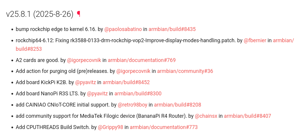 Bildquelle: https://docs.armbian.com/Release_Changelog/?ref=blog.armbian.com#v2581-2025-8-26 ### Nordic Semiconductor: Zephyr-freies SDK für nRF54L Bluetooth-SpCs aus dem Hause Nordic Semiconductor wurden in der Vergangenheit so gut wie immer unter Nutzung
Softwareprodukte an. Unter der URL https://www.cnx-software.com/2025/08/24/getting-started-with-quectel-ec200u-4g-lte-cat-1-iot-board-using-the-qnavigator-and-the-quecopen-sdk/ findet sich nun ein Tutorial, das die ersten Schritte unter Nutzung der hauseigenen SDKs zu illustrieren sucht.
RESETPATHS; BLOCK ASYNCPATHS; Refer to “Case Study 1 – No user-defined timing constraint” on page 47 for details. BLOCK PATH For identified asynchronous paths, you can use a BLOCK preference to prevent the engine and TRACE from analyzing
Life: 25 years at 21°C More Details: On-Line Catalog-Application Manual (Li2FeS ) Shipping: Please refer to PSDS Document Certifications: II 1G Ex ia IIC Ga Baseefa 14ATEX0107U (If specially marked) *All data shown tested at 21°C unless otherwise stated. Milliamp-Hours Capacity Constant Current Discharge to 0.8 Volts AA Lithium AA Alkaline 5000 ) h 4000 m ( 3000 i a 2000 p C 1000 0 0 200 400 600 800 1000 Continuous Discharge Drain (mA) Cells are tested against ANSI-19 C18.3M. (alkaline shown for comparison) Discharge Profile Temperature Effects on Capacity Constant Current Discharge
Device Pin Description Font Description DEVICES HDSP-6504 HDSP-6508 7 Cathode C Anode 5 Cathode I: 3.81 REF. (0.150) 5" REF. An Ca An An Figure8. An An An WWW4 HPARCHIVE.COM OperationalConsiderations E TI n u a r-w aa ii-6508devices utilize largemonolithic u ia a ip a w i i i ic a a i i u I I g i i i u~u
/storage/refs/refs-overview Ich habe ein normales NTFS (ohne EFI) und bei mir sind die Daten konsistent. Hier derselbe Datenträger mal "offline" mit einem anderen Windows geöffnet, um das Berechtigungsproblem
Alexander schrieb im Beitrag #7931029: > Von was reden wir hier überhaupt *.vhdx mit ReFS > kann sich vollkommen anders verhalten > als ein Plain Windows NTFS Dateisystem. Wir reden von einem Windows NTFS Dateisystem in einer VM. Meine Linux Tests habe ich wie gesagt gemacht, indem

 Bild
Bild
 Bild
Bild
 Bild
Bild
 Bild
Bild
 Bild
Bild
 Bild
Bild
 Bild
Bild