Sieht wohl so aus. Wird z.B. hier erläutert: https://community.infineon.com/t5/Knowledge-Base-Articles/Queries-on-BLE-Qualification-and-Declaration-Processes/ta-p/259951#.
https://www.we-online.com/catalog/media/o662703v410%20ANR027_Bluetooth_Listing_Guide.pdf#page16 Hier bei Würth steht einiges dazu. Die Vertreter sind diesbezüglich auch sehr gut geschult bzw. stellen den Kontakt zu den Spezialisten her. Bei euren 100..200 Modulen seid ihr dort mit Sicherheit
Base64 U. schrieb im Beitrag #7846778: > Gerade in solchen Stressigen Situationen zahlen sich einfache, robuste > Lösungen aus. ACK.
16A sind. Das mit dem Trafo geht auch aber.... Wenn man statt einem B6U einen M6U nimmt komm ich auf 312V statt 540V und hab mit den 312V und 16A genau 4992W das ist perfekt. So wirds gemacht. Danke
its own associated I/O line (CEXn) which is routed through the crossbar to port I/O when enabled. • 16-bit time base. • Programmable clock divisor and clock source selection. • Up to five independently-configurable channels • 8- or 16-bit PWM modes (edge-aligned operation). • Frequency output mode. •
acht Kontakte aufweisende WCSP-Gehäuse um 38 % kleiner als das konkurrierender Bauelemente. Neben 16 KB Speicher enthält der MCU einen dreikanaligen 12bit-A/D-Wandler und sechs GPIO-Pins (General-Purpose Input/Output) und bietet Kompatibilität zu standardmäßigen Kommunikations-Schnittstellen wie etwa
hardware socket communication at the same time Internal 32Kbytes Memory for Ethernet Tx/Rx Buffers 10BaseT/100BaseTX Ethernet PHY embedded Support Auto Negotiation (Full and half duplex, 10 and 100-based) Up to 12 communication interface 2 x I2C interfaces(support SMBus/PMBus) 5(W55MH32L) / 3(W55MH32Q
Input Power Dissipation (Each Channel) PI — 15 mW Output Current (Each Channel) IO — 60 mA Emitter Base Reverse Voltage (HCPL-4701/070A) V EB — 0.5 V Output Transistor Base Current (HCPL-4701/070A) I — 5 mA B Supply Voltage V CC –0.5 18 V Output Voltage VO –0.5 18 V Output Power Dissipation (Each Channel
the amplifier output are rectified and stored in the 5 μF capacitor. This potential is fed to the base of Q3. Q3's collector current will vary with the difference between its base and emitter voltages. Since the emitter voltage is fixed by the LM313 1.2V reference, Q3 performs a comparison function and its collector current modulates Q1's base voltage. Q1, an emitter follower, provides servo controlled drive to the Q2 oscillator. If the emitter of Q2 is opened up and driven by a control voltage, the amplitude of the circuit output may be
the amplifier output are rectified and stored in the 5 μF capacitor. This potential is fed to the base of Q3. Q3's collector current will vary with the difference between its base and emitter voltages. Since the emitter voltage is fixed by the LM313 1.2V reference, Q3 performs a comparison function and its collector current modulates Q1's base voltage. Q1, an emitter follower, provides servo controlled drive to the Q2 oscillator. If the emitter of Q2 is opened up and driven by a control voltage, the amplitude of the circuit output may be
2025-03-03 08:03:27 oder 08:03:28 2025-01-31 10:57 Freitag 2025-01-31 14:10 2024-11-22 12:16 Freitag 2024-11-25 09:31 2024-10-24 07:16 Donnerstag 2024-10-24 12:10 2024-10-08 08:28 Dienstag 2024-10-09 08:21[/pre] Der modernisierte Online Shop gefällt mir auch ganz gut, warum gibt es
ist halt wie gesagt die Verschlagwortung. Beispiel Medienkonverter: Es gibt als "Ausführung" "1000Base-T" und "1000Base-TX", beides in diversen Kombinationen mit "1000Base-X", "1000Base-SX" oder "1000Base-LX", manchmal sogar in Kombination mit der Angabe der Glasfaser-Stecker. Das ist so unübersichtlich
Derived1> (... /* Konstruktor-Parameter für Derived1 */); // virtuelle Funktionen aufrufen for (Base& obj : counters) obj.current ().exec (); // Alle löschen counters.clear (); }[/c]
einzige erzeugte Instanz schon RAM verbraucht hat. Die Objektinstanzen selbst fressen dann mindestens 16 Bytes selbst wenn sie keine lokale Variablen haben.
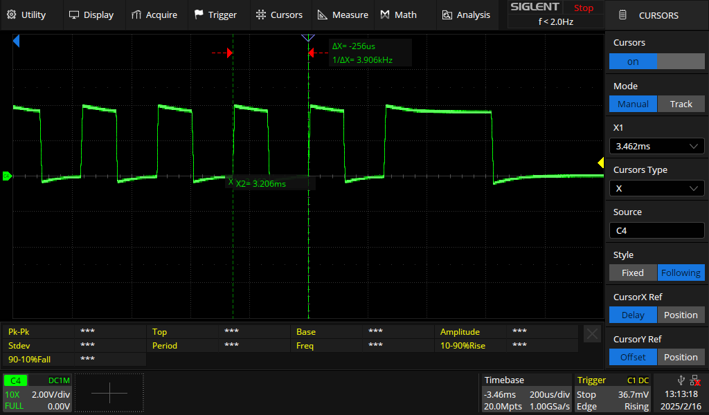
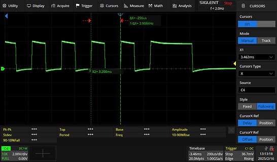
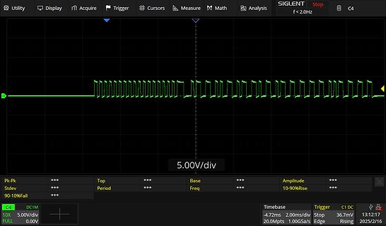
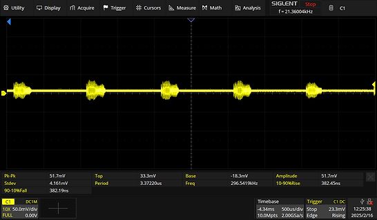
Style Fixed Following CursorX Ref Position CursorY Ref Position Pk-Pk Stdev 90-10%Fall Top Period Base Freq Amplitude 10-90%Rise G4 10X FULL DC1M 2.00V/div 0.00V Timebase -3.46ms 200us/div Trigger Stop Edge Rising C1 DC 36.7mV 13:13:18 2025/2/16
arA at T = +25°C.) 4 PARAMETER SYMBOL CONDITIONS MIN TYP MAX UNITS 7 V+ Input Voltage Range V+ 3.0 16.5 V 7 X V+ = 16.5V, SHDN ≤ 0.4V (operating) 100 Supply Current V+ = 10V, SHDN ≥ 1.6V (shutdown) 2 5 µA A V+ = 16.5V, SHDN ≥ 1.6V (shutdown) 4 M FB Trip Point 3V ≤ V+ ≤ 16.5V -10 10 mV MAX77_C ±50 FB
eine Aufnahme der Weihnachtsfeier geben, mit dem Kaufladen drauf. "Normal-8" Format, dazu wurde ein 16mm-Film in eine Kassette eingelegt und wie später die Tonband-CompactCassette nach der halben Aufnahmedauer umgedreht. Nach der Entwicklung wurde der dann der Länge nach aufgetrennt. "Super-8" kam später
Korrekturdaten und zusätzlich der Abstand zwischen den Empfängern wenn die beiden GNSS Empfänger als Base und Rover verwendet werden (also die Base die Korrekturdaten liefert). Sonst fast alles wie bei der Messung weiter oben, diesmal bei guter Rundumsicht und Bewölkung. Die Bilder im Anhang zeigen
G11 1302 G12 LT1302-5 Output Voltage vs MaximumOutput Power* Load Current Boost Mode 5.20 20 5.15 16 ) 5.10 ) ( ( G 5.05 E 12 L W V 5.00 VIN= 4V P T U P 4.95 VIN= 2.2V V = 3V T 8 U IN O O 4.90 4 4.85 4.80 0 0 0.1 0.2 0.3 0.4 0.5 0.6 0.7 0.8 0.9 1.0 0 2 4 6 8 10 LOAD CURRENT (A) INPUT VOLTAGE (V) 1302
OUT SENSE 2 8 11 OV FAULT WINDOW ADJUST 5 17 LINE/SWITCHER 9 10 OV DELAY SENSE SENSE 1 NC 6 16 POWER OK SENSE 4 INVERT 7 15 UV DELAY INPUT SENSE 4 8 14 UV FAULT 9 10 11 12 13 3 2 1 E E E A L S S S E AU E E E D F S S S V V O O ABSOLUTE MAXIMUM RATINGS (1) over operating free-air temperature range
its own associated I/O line (CEXn) which is routed through the crossbar to port I/O when enabled. • 16-bit time base. • Programmable clock divisor and clock source selection. • Up to five independently-configurable channels • 8- or 16-bit PWM modes (edge-aligned operation). • Frequency output mode. •
verspricht man in Künzelsau dann folgendes: [c] Thanks to their enlarged solder pads and thicker base plate, the capacitors can withstand acceleration up to 30 g (294 m/s²). . . . The capacitors are tested under conditions that go beyond the requirements of IEC 60384-4: The components must remain
Features finden sich unter der URL https://android-developers.googleblog.com/2025/01/first-beta-android16.html. ### Lesestoff, zur Zweiten - von EU-Regulation im Technikbereich. Die EU-Kommission steht nie still. Die internationale Anwaltssocietät Schönherr bietet unter der URL https://www.schoenherr.eu
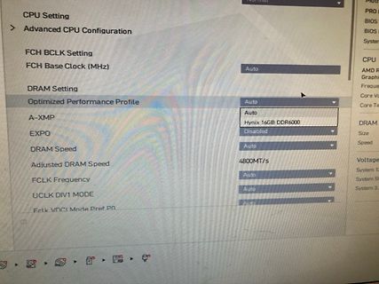
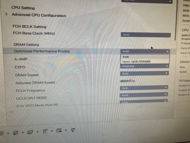
CPU Setting
Advanced CPU Configuration
FCH BCLK Setting
FCH Base Clock (MHz) Auto
DRAM Setting
Optimized Performance Profile Auto
A-XMP Hynix 16GB DDR6000
EXPO Disabled
DRAM Speed Auto
Adjusted DRAM Speed 4800MT/s
FCLK Frequency Auto
UCLK DIV1 MODE Auto
Fclk VDCI
Typedef 'Color' multiply defined. End time: 08:06:58 on Jan 28,2025, Elapsed time: 0:00:00 Errors: 16, Warnings: 1 [/c] Keine Ahnung, ob die Warnung in Zeile 16 hilfreich und berechtigt ist...
visuMon ** Warning: ../src/visuMon.sv(16): (vlog-13314) Defaulting port 'i_debugInfo' kind to 'var' rather than 'wire' due to default compile option setting of -svinputport=relaxed. -- Compiling module visuMon_tb ** Error: ../sim/visuMon_tb.sv
Signal Overvoltage No Change in Display −35 35 V VOLTAGE-DIVIDER Divider Resistance Total, Pin 6 to 4 16 28 36 kΩ Relative Accuracy (Input Change Between Any (3) Two Threshold Points) 2.0 3.0 4.0 dB Absolute Accuracy at Each Threshold Point (3) VIN = −3, −6 dB −0.5 +0.5 dB V = −9 dB −0.5 +0.65 dB IN VIN
test_v(values: ptr16, laenge: int): method = adc.read_u16 start: int = ticks_us() index: int = 0 while index < laenge: values[index] = int(method()) index += 1 stop: int = ticks_us(

 Bild
Bild
 Bild
Bild
 Bild
Bild
 Bild
Bild
 Bild
Bild
 Bild
Bild
 Bild
Bild
 Bild
Bild
 Bild
Bild