, - 4 u› ZWV s 3«3 QLem eaaeevw „SI 4gg'?~ ama - 4 : iígfiI 1øc _ „„ _ 12 _. E u m søsv mv 1šä_ “s41fiä,äzzz5_-16 -15 @E =¬s ¬f mv „,_ § _I*iWi07? E; _ ı z a s I LØWJI _šzum u m 90873 e ı Q K4s i_ 3G“ššE 8007308%
to change without notice Revision_3.4_022023 Bosch Sensortec | BMA456 Data Sheet 47 | 102 Register (0x0E) DATA_4 DESCRIPTION: AUX_Z(LSB) RESET: 0x00 DEFINITION (Go to register map): Name Register (0x0E) DATA_4 Bit 7 6 5 4 Read/Write R R
Serial.begin(115200); delay(5000); Serial.printf("core 0 started\n"); } void loop() { uint16_t val = analogRead(A0); float frequency = val; DelayTime_us = 1 / frequency * 1e6; if(DelayTime_us>100000)DelayTime_us=100000; delay(100); Serial.println(DelayTime_us); } // ######
Christoph M. schrieb im Beitrag #7851284: > uint16_t val = analogRead(A0); > float frequency = val; > DelayTime_us = 1 / frequency * 1e6; Was macht die IEEE754 Implementation wenn val == 0 ist? Und warum uint -> float -> uint? Wichtiger
(i.e. 8 adjacent arbitrary bits) at any location, and zeros otherwise, e.g. 0x00000045, 0x00045000, 0x7f800000. Any 32bit number that consists of the same byte repeated 2 or 4 times in fixed places, as in
the value where bit “x mod 32” is one, and all others are zero. To calculate the offset address “y*4”, i.e. “(x/32)*4”, the register is first shifted right by 5 bits and then shifted back left by 2 bits. This is the same as shifting 3 bits right and zeroing out the lower 2 bits; but two shift instructions
Drawing & Block Diagram 36.98¡ Ó 0.2 2.05¡ Ó 0.2 1 VSS 35.98(PLZ) 0.70 30.00 AA 1.10 2 VCC 3 VCOMH 4 VCI 5 VDD Cover Glass 6 BS1 BS2 7 s R 6 8 VSS l G ) r Z A 9 IREF 2 e P A . v ( 10 CS# 0 o 3 0 . 3 C . . 9 2 3 5 0 11 RES# . . 3 3 4 6 12 D/C 3 Pull tape 13 W/R# g 14 RD# i d e 15 D0 b n 16 D1 U IC 0
bp c D(1) E(1) e H E L Lp Q v w y Z θ 0.25 1.45 0.49 0.25 8.75 4.0 6.2 1.0 0.7 0.7 mm 1.75 0.10 1.25 0.25 0.36 0.19 8.55 3.8 1.27 5.8 1.05 0.4 0.6 0.25 0.25 0.1 0.3 o 8o 0.010 0.057 0.019 0.0100 0.35 0.16 0.244
document is subject to legal discNexperia B.V. 2020. All rights reserved Product data sheet Rev. 7 — 16 April 2020 9 / 14 Nexperia 74HC08; 74HCT08 Quad 2-input AND gate TSSOP14: plastic thin shrink small outline package; 14 leads; body width 4.4 mm SOT402-1 D E A X c y HE v M A Z 14 8 Q A 2 (A3) A pin
Current Figure 4: Maximum Forward Current vs. Ambient Temperature 14.0 16 c 12.0 A 14 m m - - 12 I )10.0 N S A E E 3 R 10 T T 8.0 U I A C S E C 8 O I 6.0 D I L L 6 M M B U R 4.0 A L O O 4 I ( L T A L 2.0 X 2 E A R M
multiplexers and switches may exceed this capacitance because they connect multiple paths together. s 1 4 e l r 0 4 g m 2 7 s a 0 f e u 6 e a 4 4 . l xxxxxxxxxxxxxxxxxxxxx xxxxxxxxxxxxxxxxxxxxxxxxxx xxxxxxx x x x xxxxxxxxxxxxxxxxxxxxxxxxxxxxxx xxxxxxxxxxxxxxxxxxx xx xx xxxxx xxxxxxxxxxxxxxxxxxxxxxxxxxx xxxxxxxxxxxxxxxxxxx
EF6 EF5 4AD — 24LC256 — 24LC256 4L256T 24LC256T 24LC256 EF4 EF3 4LD — 24FC256 — 24FC256 4F256T 24FC256T 24FC256 EF8 — 4FD AAFKYY Legend: XX...X Part number or part number code T Temperature (I, E) Y Year code
determine the maximum supply voltage the following parameters must be considered. Add the dropout voltage (4V for LM3886) to the peak output swing, V opeak to get the supply rail value (i.e. ± (opeak+ Vod) at a current of Iopeak). The regulation of the supply determines the unloaded voltage, usually about 15%
VN5E016AH-E 16 mΩ high-side driver with analog current sense for automotive applications Features Max supply voltage V CC 41V Operating voltage range V 4.5 to 28V CC Max on-state resistance (per ch.)R ON
fast thermal transients TTSD T HYST T R TJ_START T J Power Limitation ILimH> < ILimL I OUT 18/34 VND5E160J-E Electrical specifications 2.5 Electrical characteristics curves Figure 15. Off state output current Figure 16. High level input current Iloff (nA) Iih (µA) 300 5 4,5 Vin=2.1V 250 Off State Vcc=
100 125 150 175 0 s Tc (ºC) 0 5 10 15 Vcc (V) 25 30 t5( 40 u c Figure 15. Input high level Figure 16. Input hysteresis voltage d r o Vi4 (V) Vhyst (V) P 3.8 1.5 e 3.6 1.4 e t 3.4 1.3 l s.2 o 3.2 b 1.1 3 O 1 2.8 - 0.9 2.6 s ) 0.8 2.4 t ( 0.7 2.2 c 0.6 2 d u 0.5 -50 -25 0 25 Tc (ºC)5 100 125 150 175 -
4) See Figure 16 V/µs 8/27 Doc ID 10896 Rev 4 VN920SP-E Electrical specifications Table 7. Logic inputs Symbol Parameter Test conditions Min. Typ. Max. Unit VIL Input low level voltage 1.25 V IIL Low level
C C ADBUS0 16 Y L R R R I I I I 17 49 E E E O O O O ADBUS1 18 VREGOUT ADBUS2 19 ADBUS3 21 ADBUS4 22 ADBUS5 23 ADBUS6 24 ADBUS7 ACBUS0 26 7 DM ACBUS1 27 8 DP ACBUS2 28 ACBUS3 29 6 REF ACBUS4 30 ACBUS5 32 14 33 RESET
Adam P. schrieb im Beitrag #7843910: > Muss nicht 100% genau sein, ich denke mal so 2-4% Genauigkeit. > Temperatur wird wohl so zwischen 20°C - 50°C liegen. Die mittlere Temperatur läge dann bei grob 300K, so dass du mit 2-4% bei Abweichungen von bis zu 12K landest. Hört sich machbar
würde ich lieber PT1000 verwenden, wenn das Gerät sehr lange halten soll. Die NTCs entwickeln nach m.E. nach >10 Jahren doch eine merkliche Drift.
einem STM32U0 verwendet. 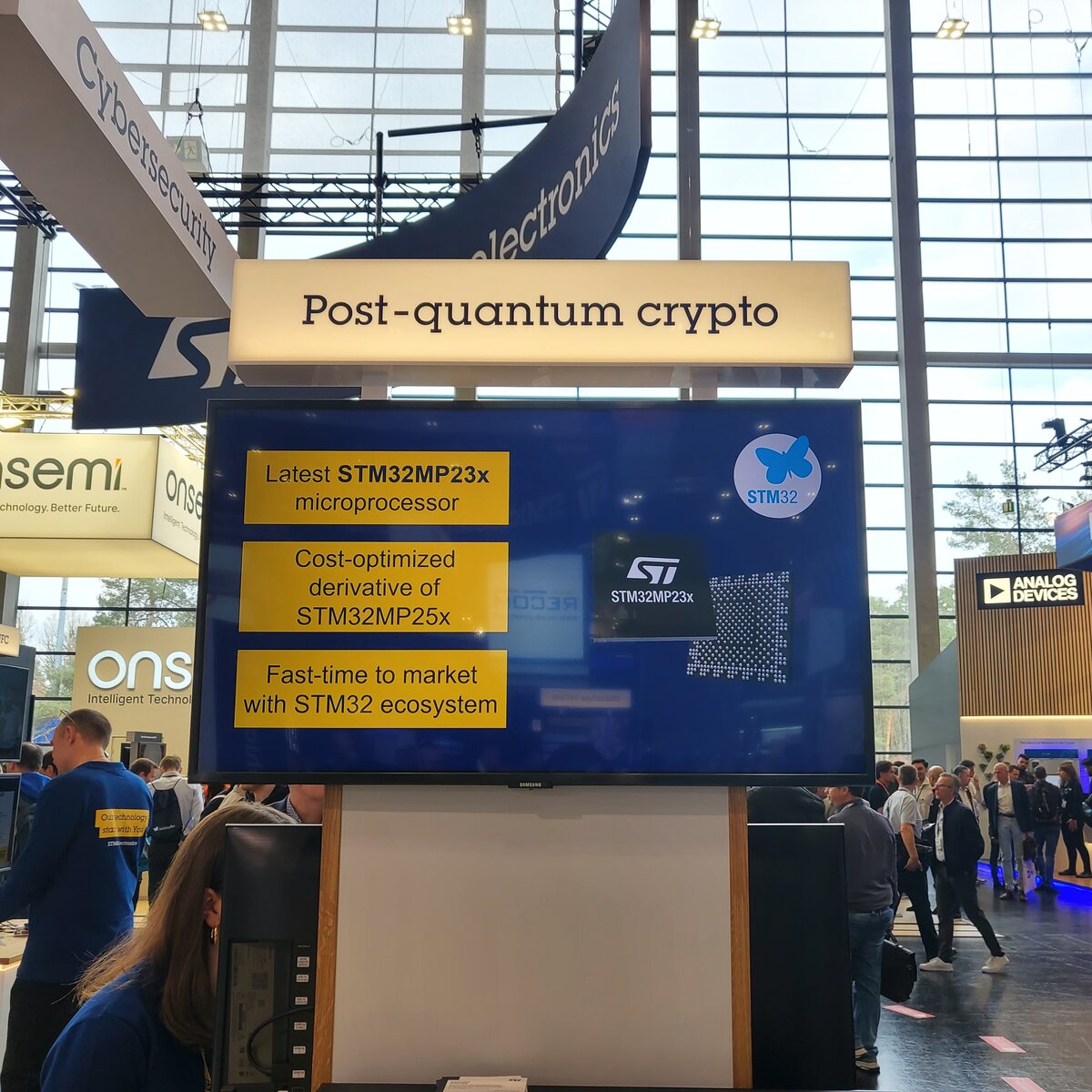 ### Espressif – QWERTZ-Tablet mit ESP32-P4, PLCs, ESP32-H4-Demo Espressif zeigte sich in Sachen Neuankündigungen gar nicht faul. Eine Demo des H4 bewies, dass es sich dabei nicht um Vaporware handelt. 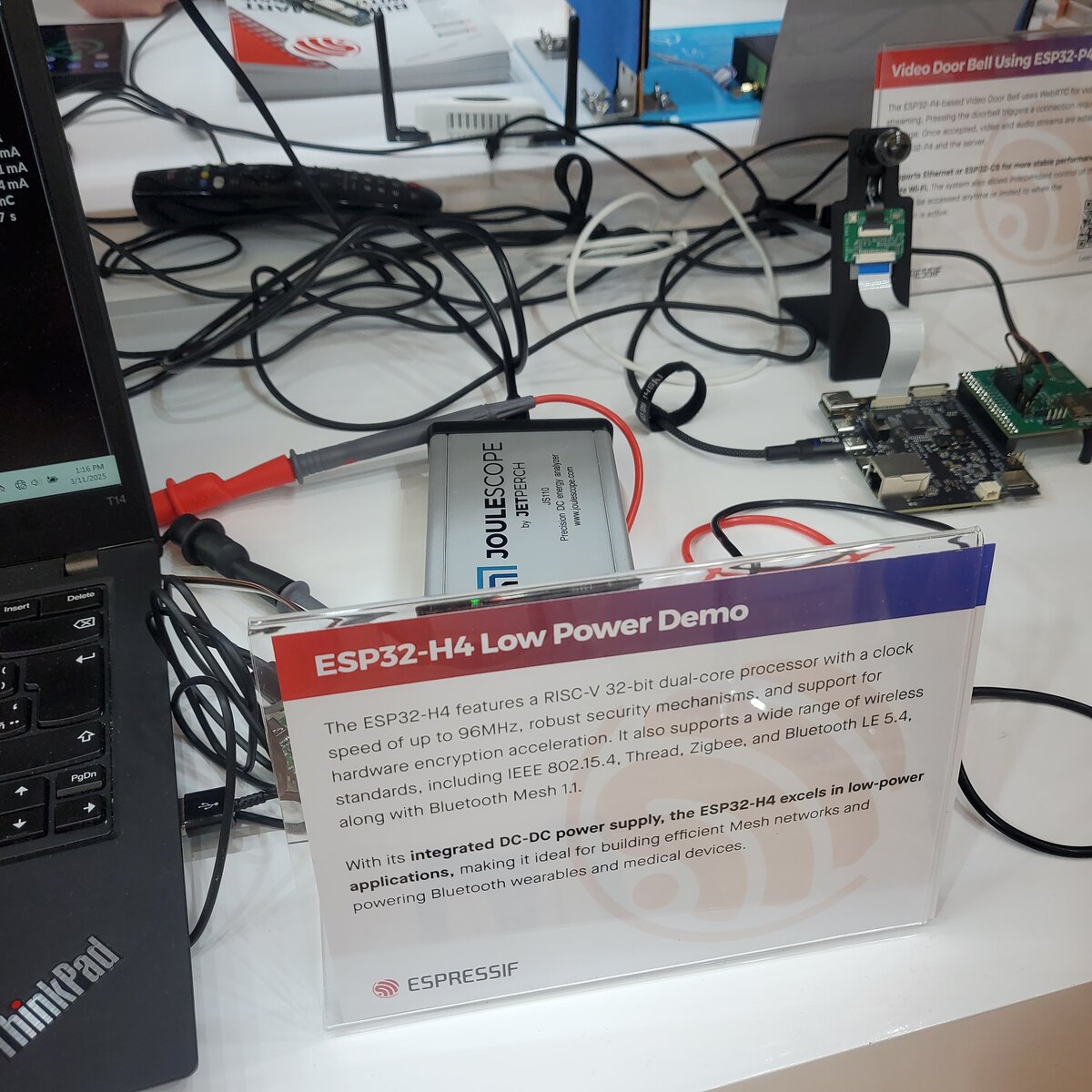 Der
Shutdown Current vs Junction IN IN Temperature 50 1.09 VO = 1.05 V 45 1.08 40 35 A ) 1.07 ( ( n 30 e r t u 25 o 1.06 t t p p I 20 u E O 15 1.05 10 1.04 5 VIN= 5 V VIN= 12 V VIN = 12 V VIN= 18 V 0 1.03 0 5 10 15 20 0 0.5 1 1.5 2 2.5 3 3.5 4 4.5 5 5.5 EN Input Voltage (V) Output Current (A) G002 G004
Microsystems Plc 3 D/602B/2 Calling Line Identifier CMX602B 1.3 Signal List Packages Signal Description D4/P3/E4 Pin No. Name Type 1 XTALN O/P The output of the on-chip Xtal oscillator inverter. 2 XTAL I/P The input to the on-chip Xtal oscillator inverter. 3 RD I/P (S) Input to the Ring or Line Polarity Reversal
ziemlich sinnlos. Die sollte auch mehr als ein paar Minuten überbrücken. Mit einem uC, TCXO und u-blox SAM-10Q reicht eine 18650-Zelle für viele Stunden, das sollte noch passen. Mit 4 NOR-Flash Speicherchips braucht der uC kaum RAM und man kann 127 Tage lang jeden Tag 2MByte Rohdaten speichern. Oder ein
almost instantaneous. For a 0V–10V input the output will run over 1 Hz to 30 kHz with less than 0.4% distortion. In addition, linearity of control voltage vs output frequency will be within 0.25%. Figure 16 shows the response of this circuit (waveform B) to a 10V ramp (waveform A). SNOA665C–October
almost instantaneous. For a 0V–10V input the output will run over 1 Hz to 30 kHz with less than 0.4% distortion. In addition, linearity of control voltage vs output frequency will be within 0.25%. Figure 16 shows the response of this circuit (waveform B) to a 10V ramp (waveform A). SNOA665C–October
C) Figure 1. On−Region Characteristics Figure 2. Gate−Threshold Voltage Variation With Temperature E A 20 L 2 25°C V N ) W VGS = 0 S 16 TJ= −55°C D 1.6 M 100°C A ID= 0.25 mA ( E ) N 12 B E1.2 R C L R R A C O R I 8 − ON0.8 R T ( , N ID VDS = 20 V A 4 D 0.4 ,) S 0 ( 0 0 4 8 12 16 20 B −50 −75 0 25 50
Sam schrieb im Beitrag #7836638: > Aber sind 16 GB zu viel für HA? Oder bin ich > trotzdem sicher? RAM beim Computer ist wie Hubraum beim Auto, es gibt kein "zuviel" ;-)
Sam schrieb im Beitrag #7836638: > ... Mir ist aufgefallen, dass kürzlich > eine 16-GB-Variante des Pi 5 veröffentlicht wurde. > https://electronicsforyou.com/de/produkte/raspberry-pi-5-16gb-ram/
C C ADBUS0 16 Y L R R R I I I I 17 49 E E E O O O O ADBUS1 18 VREGOUT ADBUS2 19 ADBUS3 21 ADBUS4 22 ADBUS5 23 ADBUS6 24 ADBUS7 ACBUS0 26 7 DM ACBUS1 27 8 DP ACBUS2 28 ACBUS3 29 6 REF ACBUS4 30 ACBUS5 32 14 33 RESET
values. 003aaa037 10 003aaa038 1 I ITSM T(RMS) T (A) ITSM 0.8 (A) 8 T time o 6 Tjinitial = 25 C max 0.6 4 0.4 0.2 2 0 0 0 20 40 60 80 100 120 140 1 10 102 n 103 o Tlead ( C) n = number of cycles at f = 50 Hz Fig 4. Maximum permissible non-repetitive peak Fig 5. Maximum permissible RMS current as a on-state
nie angezeigt werden - Wert 2 bedeutet NMI Interrupt - Wert 3 bedeutet HardFault Usw. - Werte ab 16 sind die "normalen" Interrupts, also die die von der Peripherie ausgelöst werden. Bei deinem Controller sind diese hier definiert, auf die dortige Angabe von "Line" musst du 16 aufaddieren: https://onlinedocs.microchip.com/oxy/GUID-F5813793-E016-46F5-A9E2-718D8BCED496-en-US-14/GUID-DA8CB38A-18D7-4512-965B-BB439142B281.html Heißt also, IPSR=16 ist PM - Power Manager Interrupt, IPSR=17 ist MCLK - Main Clock usw. Alex schrieb im Beitrag
A U Shelf life (at 105 C) After 1000 hours no load test, leakage current, capacitance and tan are same as load life value. R E T DRAWING Unit : mm Y P E S Insulating sleeve d 0.05 Tinned copper-ply wire x D 5 6.3 8 10 12.5 16 18 22 25.4 m P 2.0 2.5 3.5 5.0 5.0 7.5 7.5 10.0 12.5 . P 0.5 0 d 0.5 0.5 0.6
/COM2 COM1 Port, COM2 Header DIMMA1 Slot DIMMB1 Slot DIMMA2 Slot DIMMB2 Slot Total System Memory 5 E A1SAi/A1SRi Series Motherboard 5 0 Rev. 1.00 U FAN1 - FAN3 CPU and System Cooling Fans 4GB 4GB - JI2C2 8 B L B - 4GB 4GB 8GB r A A 2 IPMI LAN Dedicated IPMI LAN Port N C A 0 JBT1 4GB 4GB 4GB 4GB 16GB M d 1 J1* 4-pin 12V DC Power Connector (To provide alternative power for the 8GB 8GB 16GB e special enclosure when the 24-pin ATX power is not in use.)* n d 8GB 8GB 8GB 8GB 32GB i e 1 w n J3 4-pin Power Connector
