-
PDF
6502_Schematic.pdf
Cp2 Cp2 A7 x8 DATA1 x1 Cp1 x2 x2 x3 x4 x5 x6 x7 Cp2 Carry7,out ADDR1 Cp2 Carry ADDR2 x3 Cp2 x5 x7 1. op. Cp2 DATA2 x4 ADDR2 DATA1 x1 x0 Carry 2. op. x3 DATA1 x1 ADDR2 x1 x5 D6 x1 x3 Carry x3 x2 SUM EOR NOR x2 x2 x4 DATA1 x12 x9 x3 Cp2 Cp2 ADDR1 x6 x3 ADDR1 x2 x4 XOR7 x15 ADDR1 Cp2 x4 x20,6 ALU6 x14 DATA2
in „LED Lauf-/Blinklicht in DIY Spielzeug“ · Analoge Elektronik und Schaltungstechnik ·
-
PDF
ad620.pdf
accuracy. is because a three op amp type in amp has two op amps at its Regardless of the system it is being used in, the AD620 provides inputs, both contributing to the overall input error. greater accuracy, and at low power and price
in „Verständnisproblem Beschaltung Instrumentenverstärker“ · Analoge Elektronik und Schaltungstechnik ·
-
PDF
TB12To5.pdf
TT=1.84973E-007 BV=1000 IBV=0.2 Iave=1 Vpk=1000 type=silicon .model ZPD5V6 D(IS=1E-11 RS=6.168 N=1.27 TT=5E-8 CJO=3.766E-10 VJ=0.75 M=0.33 BV=5.477 IBV=0.01 Iave=500m Vpk=5.6 mfg=Motorola type=zener) Als Modell der Diode habe ich nur die UF4007 anstelle der UF4004, sie unterscheiden sich jedoch nur in
in „Diskreter DC/DC-Wandler in LtSpice“ · Analoge Elektronik und Schaltungstechnik ·
-
PDF
mcp23008.pdf
Inc. MCP23008/MCP23S08 2 FIGURE 1-1: MCP23008 I C™ DEVICE PROTOCOL S - START SR - RESTART DIN DIN S OP W ADDR .... P P - STOP w - Write SR OP R DOUT .... DOUT P R - Read OP - Device opcode SR OP W DIN .... DIN P ADDR - Device address P DOUT - Data out from MCP23008 DIN - Data into MCP23008 S OP R DOUT .... DOUT P SR OP R DOUT ....DOUT P DIN ....DIN SR OP W ADDR P P Byte and Sequential Write Byte S OP W ADDR DIN P DIN SequentialS OP W ADDR DIN .... P Byte and Sequential Read Byte S OP R SR OP R DOUT P SequentiaS OP
in „MCP23008 Problem“ · Mikrocontroller und Digitale Elektronik ·
-
PDF
ELV_Hochleistungs-Netzteilplatine.pdf
ker IC7 1ker 0 40Vu ker 1 8 4 1 2 - 3 10 1 2 A 9 C A + C27 3 + CD4011 CD4011 D16 LMR75 1u IC7 IC7 100V 1M 5 12 1N4148 D24 8 4 11 7 0 7 0 1 7 0 6 13 5 k 1 k 2 k R 1 R 1 N R 1 B D R 3 R 0 R 0 1 D26 8 1 1 17 0 C37 CD4011 CD4011 8 k +5V IC6 NR 2 R 1 D17 1 +5V 1
in „ELV Hochleistungsnetzteilplatine“ · Mikrocontroller und Digitale Elektronik ·
-
PDF
37838_Netzteil_NT30V_10A_KM_um_1_.pdf
IC7 ker 0 40V ker 1 8 4 3 10 1 2 - 2 9 1 A C A + C27 3 + CD4011 CD4011 D16 LR758 100V 1M IC7 IC7 1N4148 5 12 k D24 4 4 11 7 8 7 0 4 7 0 6 13 5 k 1 k 2 k R 1 R 1 1 R 1 B D R 3 R 1 R 1 D26 8 1 7 0 C37 CD4011 CD4011 8 k +5V IC6 N R 2 R 10 D17 D23 D25 1 +5V
in „Frage zu ELV Netzteil“ · Analoge Elektronik und Schaltungstechnik ·
-
PDF
uCurrentArticle.pdf
in this application is the near- zero offset voltage. And not just “low offset” like many precision op-amps, this one has almost no practical offset voltage at all. 0.1uV typical, with a maximum figure of 2.5uV over the entire temperature range, if you want to know the actual numbers. This class of op-amps
in „Strom im mA Bereich mit Oszi messen“ · Mechanik, Gehäuse, Werkzeug ·
-
PDF
Freq-Spannungswandler.pdf
output swings to ground for a with variable reluctance magnetic pickups t zero frequency input. n Op amp/comparator has floating transistor output o The op amp/comparator is fully compatible with the tachom- n 50 mA sink or source to operate relays, solenoids, V eter and has a floating transistor as
in „LM2907/17 Frequenz-Spannungswandler“ · Analoge Elektronik und Schaltungstechnik ·
-
PDF
Freq-Spannungswandler.pdf
output swings to ground for a with variable reluctance magnetic pickups t zero frequency input. n Op amp/comparator has floating transistor output o The op amp/comparator is fully compatible with the tachom- n 50 mA sink or source to operate relays, solenoids, V eter and has a floating transistor as
in „Frequenz Spannungswandler“ · Analoge Elektronik und Schaltungstechnik ·
-
PDF
NSC.pdf
output swings to ground for a with variable reluctance magnetic pickups t zero frequency input. n Op amp/comparator has floating transistor output o The op amp/comparator is fully compatible with the tachom- n 50 mA sink or source to operate relays, solenoids, V eter and has a floating transistor as
in „Frequenz Spannungswandler Beschaltung“ · Mikrocontroller und Digitale Elektronik ·
-
PDF
n2pk_ad8307_power_meter.pdf
than 10 dB (1.9:1 SWR) in normal input range corresponds to a mainline combination of powering, the op amp operation and higher than 20 dB (1.2:1 power range of -55 dBW to +25 dBW. input polarities and gains, and the ground SWR) in some cases. As you can see, Converting from dBW to watts results in referenced
-
PDF
10134fd.pdf
single supply designs, operation, i.e., when the negative supply is 0V. Input such as the LM124, LM158, OP-20, OP-21, OP-220, commonmoderangeincludesground;theoutputswings OP ‑ 221, OP‑420: withinafewmillivoltsofground.Singlesupplyoperation, a) When the input is more than a diode drop below however, can create
in „LT1013 Unterschied D und P Package“ · Analoge Elektronik und Schaltungstechnik ·
-
PDF
BUF634_Datasheet.pdf
resistor of 10 to 150 in series with the output. and bypass the power supplies with 0.1 F ceramic chip V+ OP AMP RECOMMENDATIONS OPA177, OPA1013 Use Low IQmode. G = 1 stable. (1) OPA111, OPA2111 C1 OPA121, OPA234 ,1) OPA130(1) VO OPA BUF634 OPA27, OPA2107 Low IQmode is stable. IncreasiLg C may cause VIN OPA602
in „OP Ausgang -> Leitung -> AD Messkarte -- Wie\Wo terminieren?“ · Analoge Elektronik und Schaltungstechnik ·
-
PDF
DAC80.pdf
IOUT – protection diodes when a high voltage op amp is used. 0 to RO 2mA I 6.6k The feedback resistor, R F, should have a temperature coef- ficient as low as possible. Using an external feedback 21 Common resistor, overall drift of the circuit increases
in „Ersatz für DAC80 (12-Bit DIGITAL-TO-ANALOG CONVERTERS)“ · Mikrocontroller und Digitale Elektronik ·
-
PDF
Schwingkond-53278649.pdf
1.1a. Alternatively, an op-amp can be configured as a parametric amplifier by using a parametric device (typically a vibrating capacitor) with the op-amp, as shown in Figure 1.lb. When a differential measurement is required, an
in „DC-Messverstärker (Chopper) mit Kapazitätsdioden (diskret)“ · Analoge Elektronik und Schaltungstechnik ·
-
PDF
tas5558-eight_channel_audio_processor_with_PWM_Output.pdf
REGISTER FIELD CONTENTS INITIALIZATION GAIN COEFFICIENT VALUE DECIMAL HEX b0coefficient u[31:28], b0[27:24], b0[23:16], b0[15:8], b0[7:0] 1.0 0x00, 0x80, 0x00, 0x00 b coefficient u[31:28], b1[27:24], b1[23:16], b1[15:8], b1[7:0] 0.0 0x00, 0x00, 0x00, 0x00 1 b2coefficient u[31:28], b2[27:24], b2[23:16],
-
PDF
INA102.pdf
. Using op amps provides gain accuracy and common-mode rejection when the INA102 is operated over wide temperature ranges. oftenleadstodesigntradeoffswhenitisnecessarytoamplify low-level signals in the presence
in „Pulsmessung und Anzeige der Pulswelle auf einem LCD Display“ · Mikrocontroller und Digitale Elektronik ·
-
Datei
MCP6001.txt
temperature, improved output stage, * fixed overdrive recovery time * REV E: 27-Jul-07, Updated output impedance for better model stability w/cap load * * Recommendations: * Use PSPICE (other simulators may require translation) * For a quick, effective design, use a combination
in „ltspice problem“ · Analoge Elektronik und Schaltungstechnik ·
-
Datei
MCP6001.txt
*************************************************************** * * Macromodel for the MCP6001/2/4 op amp family: * MCP6001, MCP6001R, MCP6001U, MCP6002, MCP6004 * * Revision History: * REV A: 21-Jun-02, Created model * REV B: 16-Jul-02, Improved output stage * REV C: 03-Jan-03, Added MCP6001 * REV D
in „MCP6001 LTspice“ · Analoge Elektronik und Schaltungstechnik ·
-
Datei
MCP6001.txt
*************************************************************** * * Macromodel for the MCP6001/2/4 op amp family: * MCP6001, MCP6001R, MCP6001U, MCP6002, MCP6004 * * Revision History: * REV A: 21-Jun-02, Created model * REV B: 16-Jul-02, Improved output stage * REV C: 03-Jan-03, Added MCP6001 * REV D
in „Einbinden opv in LT-Spice“ · Analoge Elektronik und Schaltungstechnik ·
-
Datei
MCP6001.txt
temperature, improved output stage, * fixed overdrive recovery time * REV E: 27-Jul-07, Updated output impedance for better model stability w/cap load * * Recommendations: * Use PSPICE (other simulators may require translation) * For a quick, effective design, use a combination
in „Einbinden opv in LT-Spice“ · Analoge Elektronik und Schaltungstechnik ·
-
Datei
MCP6001.txt
*************************************************************** * * Macromodel for the MCP6001/2/4 op amp family: * MCP6001, MCP6001R, MCP6001U, MCP6002, MCP6004 * * Revision History: * REV A: 21-Jun-02, Created model * REV B: 16-Jul-02, Improved output stage * REV C: 03-Jan-03, Added MCP6001 * REV D
in „OPV-Schaltung in LT Spice nicht stabil“ · Analoge Elektronik und Schaltungstechnik ·
-
PDF
tas5504.pdf
GAIN COEFFICIENT VALUE DESCRIPTION REGISTER FIELD CONTENTS DECIMAL HEX b Coefficient u(31:28), b0(27:24), b0(23:16), b0(15:8), b0(7:0) 1.0 0x00, 0x80, 0x00, 0x00 o b1Coefficient u(31:28), b1(27:24), b1(23:16), b1(15:8), b1(7:0) 0.0 0x00, 0x00, 0x00, 0x00 b Coefficient u(31:28), b2(27:24), b2(23:16),
in „[V] diverse Bauteile (Fets, BMS-ICs, Motor-Treiber“ · Markt ·
-
PDF
512020-sp-01-en-Switching_Power_Supply_DPS-4005PFC.pdf
A10 DQ6 18 AD6 15pF A11 25 1A12 R31 74HC373 1A12 2 A11 DQ7 19 AD7 A12 26 1A13 1A13 26 A12 DQ8 A13 27 1A14 1A14 27 A13 A14 28 1A15 1 1A15 1 A14 A15 RESPACK7 A15 GND X18 P0 1 LCD.C GND 20 E 1 P1 2 LCD.D 22 G/VPP 2 FAN P2 3 FLY1 VCC P3 4 FLY2 AT27c512R P4 5 RXD R9 6 TXD R6 R4 R28 R12 GND HA1 P5 7 INT0
-
 Bild
Bild
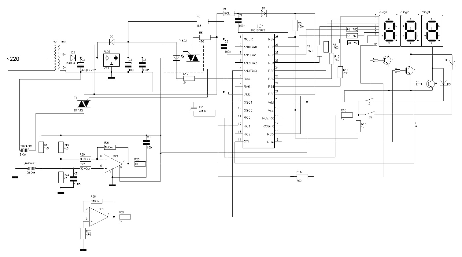
Schaltplan mit Mikrocontroller und 7-Segment-Anzeige
R9 750 R10 750 R13 750 R16 750 R17 750 R20 330k R21 1M R22 750 R23 750 R24 20 Ohm R25 750 R26 1M R27 1k R28 47u C6 100n C7 100n T4 BTA12 S1 S2 Vdd Vss AN0 bis AN4 RA0 bis RA5 RC0 bis RC6 OP1 OP2
in „Weller WSD81 Fehlermeldung“ · Mechanik, Gehäuse, Werkzeug · · Schaltpläne
-
PDF
ixTDM-Bauteile-v1.1.pdf
CSD 10‐080120 100 1 0,01 0,01 optional RS485 Buchsenleiste 10pol gewinkelt 1 CSD 014‐B110W 10 2,7 0,27 0,27 für Erweiterungen R 0603 0 2 CSD 10‐060000 100 1 0,01 0,02 wenn kein RS485 R 0603 100 1 CSD 10‐060100 100 1 0,01 0,01 R 0603 1M 2 CSD 10‐06M001 100 1 0,01 0,02 Audio In R 0603 1k 1 CSD 10‐06K001
in „Sammelbestellung? Mini-Platine: 3 Kanal Power-PWM mit ATMega+IR+RS485“ · Mikrocontroller und Digitale Elektronik ·
-
Datei
ESP32_C3_SPI_ADXL380_Analog_Devices.ino
uint16_t mode1 = readRegister(0x26); Serial.print("Mode_1: "); Serial.println(mode1); writeRegister(0x27, 0b11100000); //0x27 = DIGITAL ENABLE Reg / -> x-, y-, z-Achse and Temperatur = 1111, FIFO = 0, Double Speed = 0, INT01_EVENT = 0, PARITY_EN = uint16_t dig_En = readRegister(0x27); Serial.print("Dig_En: "); Serial.println(dig_En); writeRegister(0x26, 0b00001100); //0x26 = OP_Mode-Reg. / -> 4G == 00 , PDM = 0, Audio = 0, High Performance Mode = 1100 uint16_t mode2 = readRegister(0x26); Serial.print("Mode_2: "); Serial.println(mode2); //Status uint16_t status0 = readRegister
in „ADXL380 mit SPI auslesen“ · Mikrocontroller und Digitale Elektronik ·
-
PDF
dm9161-ds-f05_091008.pdf
10/100Mbps FastEthernetPhysicalLayer TX/FXSingleChipTransceiver 5.7 Table A (Media Type Selection) OP2 OP1 OP0 Function 0 0 0 Dual Speed 100/10 HDX 0 0 1 Manually Select 100FX HDX 0 1 0 Manually Select 100FX FDX 0 1 1 Manually Select 10TX HDX 1 0 0 Manually Select 10TX FDX 1 0 1 Manually Select 100TX
in „Beschaltung VICOM DM9161CEP“ · Mikrocontroller und Digitale Elektronik ·
-
PDF
CS8130.pdf
Register RAT3 RAT2 RAT1 RAT0 Reset (R) 0 0 0 0 BIT NAME VALUE FUNCTION RAT3-0 Receiver ASK 0000 0 R +0.27 s to -0.27 s window (500 kHz ASK mode) Timing Sensitivity. 0001 1 +0.27 s to -0.54 - 0.27 s window Timing window = 0010 2 +0.27 s to -1.08 - 0.27 s window +0.27 s to ↓ ↓ ↓ -RAT(2/3.6864E06) 1111 15 +0.27 s to -8.14 - 0.27 s window - 0.27 s The timing window is relative to the modulation divider register nominal setting. Register 28, CS8130 Silicon Revision Register D3 D2 D1 D0 Register REV3 REV2 REV1
-
 Bild
Bild
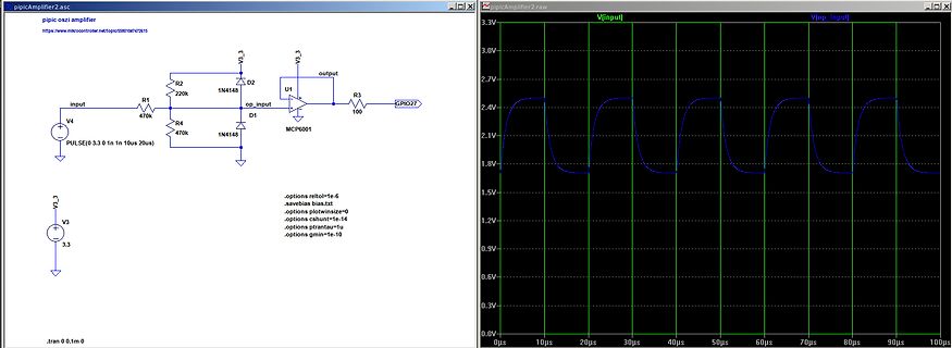
Schaltplan und Oszilloskop-Simulation eines Pips Amplifier
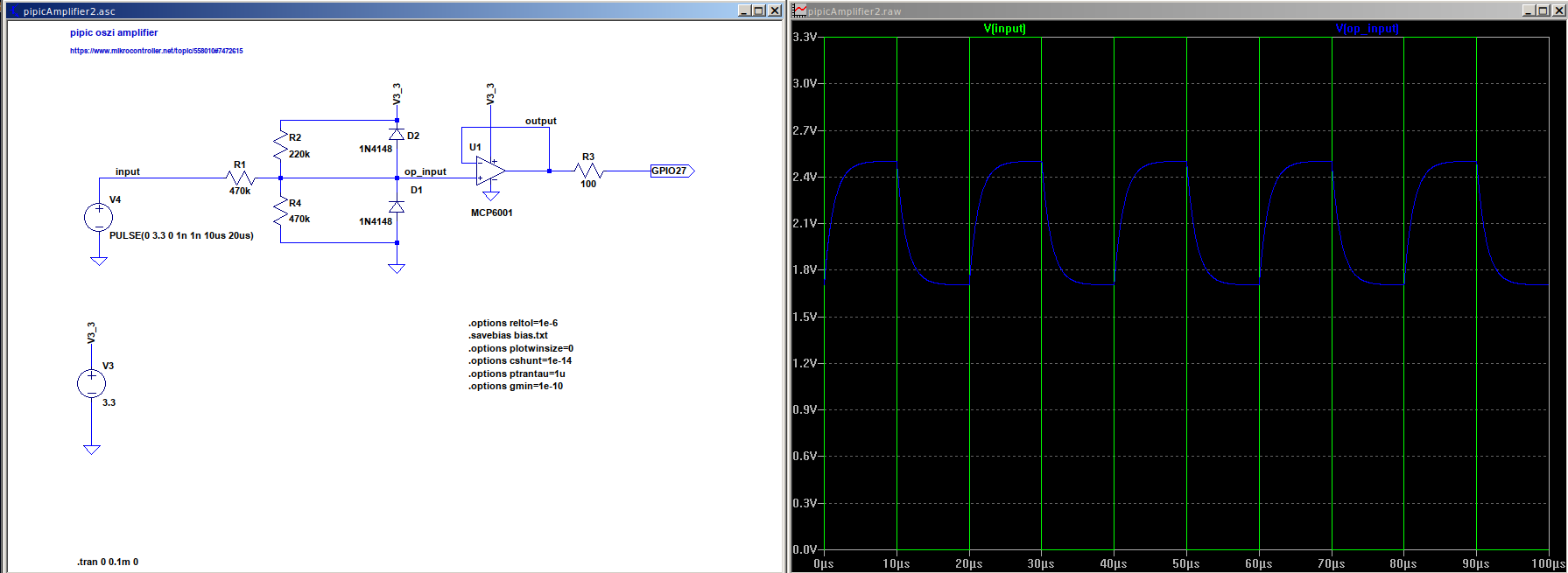
input V4 PULSE(0 3.3 0n 1n 10us 20us) R1 470k R2 220k V3_3 1N4148 D1 D2 470k R4 1N4148 U1 MCP6001 op_input output R3 100 GPIO27 V3 3.3 .tran 0 0.1m 0 .options reltol=1e-6 .savebias bias.txt .options plotwin=1e-14 .options column=1e-14 .options ptranau=1e-10 .options gmin=1e-6 [graph] V[input] V[op_input
in „PiPico Oszilloskop“ · Offtopic · · Screenshots
-
PDF
LTC1859.pdf
LTC1857/LTC1858/LTC1859 Simplified Equivalent Circuit A + CH0 LT1792: Single, low noise JFET input op amp, ±5V IN 3000pF supplies. A – IN CH1 • LT1793: Single, lownoise JFET input op amp, 10pAbias • current, ±5V supplies. + MUXOUT LT1881/LT1882:Dualandquad,200pAbiascurrent,rail- MUXOUT – + to-rail output op amps. Up to ±15V supplies. ADC ADC– LT1844/LT1885:Dualandquad,400pAbiascurrent,rail- 1859 F02 to-rail output op amps. Up to ±15V supplies. Faster Figure 2. Analog Input Filtering response and settling
in „LTC1859 merkwürdige Messwerte“ · Mikrocontroller und Digitale Elektronik ·
-
Datei
8080int-jmp.asm
,ZFL_C ; | rjmp op_da_a02 ; if (C flag ... cpi opl,0x90 ; |... or upper nibble >= 0x90) brlo op_da_a03 ; | op_da_a02: ori oph,0x60 ; add 0x60 ori temp2,(1<<ZFL_C) ; set new C flag op_da_a03: ; endif rjmp op_da_ae op_da_a10
in „CP/M auf ATmega88“ · Mikrocontroller und Digitale Elektronik ·
-
Datei
lcdcon.asm
def eins=r1 .def HN=r2 .def LN=r3 .def temp=r16 .def temp2=r17 .def temp3=r18 .def Bits=r19 .def NextOp=r20 .def tempm=r21 .def Spalte=r25 .def XAdresseLow=r26 .def Zeile=r27 .def AdresseLow =r30 .def AdresseHigh=r31 ;PortB .equ EnLCD=0 .equ Command=1 ;PortD .equ XSCL=3 .equ LP=4 .equ FLM=5 .org 0000 rjmp
in „Interrupts beim mega8515“ · Mikrocontroller und Digitale Elektronik ·
-
Datei
basiclcdcon.asm
def eins=r1 .def HN=r2 .def LN=r3 .def temp=r16 .def temp2=r17 .def temp3=r18 .def Bits=r19 .def NextOp=r20 .def tempm=r21 .def Spalte=r25 .def XAdresseLow=r26 .def Zeile=r27 .def AdresseLow =r30 .def AdresseHigh=r31 ;PortB .equ EnLCD=0 .equ Command=1 ;PortD .equ XSCL=3 .equ LP=4 .equ FLM=5 .org 0000 rjmp
in „Altes Grafikdisplay (monocrome)“ · Mikrocontroller und Digitale Elektronik ·
-
Datei
Opcode_Rom.vhd
PC_WIDTH)-1; type Rom is array (0 to (2**PC_WIDTH)-1) of std_logic_vector(DATAWIDTH-1 downto 0); -- Op_A_sel(3) | Op_B_sel(3) | Op_Load_sel(3) | Operation(5) | MAC Shift(3) | Ram Adr_A(6) | Ram Adr_B(6) | Ram Adr Write(6) constant Parameter_Rom : Rom := ( --load and store parameter "11011011000010000000000000000000000
in „Timing Constraints mit negativen Zeiten“ · FPGA, VHDL & Co. ·
-
Datei
8080int-jmp.asm
,(1<<ZFL_C) rjmp op_da_60 cpi opl,0xa0 brlo op_da_60n op_da_60: ori oph,0x60 op_da_60n: cpi opl,0x9a brlo op_da_99n ori z_flags,(1<<ZFL_C); set C op_da_99n: sbrs z_flags,ZFL_N ; if sub-op rjmp op_da_add ; then sub opl,oph
in „CP/M auf ATmega88“ · Mikrocontroller und Digitale Elektronik ·
-
Datei
8080int-jmp.asm
,(1<<ZFL_C) rjmp op_da_60 cpi opl,0xa0 brlo op_da_60n op_da_60: ori oph,0x60 op_da_60n: cpi opl,0x9a brlo op_da_99n ori z_flags,(1<<ZFL_C); set C op_da_99n: sbrs z_flags,ZFL_N ; if sub-op rjmp op_da_add ; then sub opl,oph
in „CP/M auf ATmega88“ · Mikrocontroller und Digitale Elektronik ·
-
Datei
8080int-jmp.asm
,(1<<ZFL_C) rjmp op_da_60 cpi opl,0xa0 brlo op_da_60n op_da_60: ori oph,0x60 op_da_60n: cpi opl,0x9a brlo op_da_99n ori z_flags,(1<<ZFL_C); set C op_da_99n: sbrs z_flags,ZFL_N ; if sub-op rjmp op_da_add ; then sub opl,oph
in „CP/M auf ATmega88“ · Mikrocontroller und Digitale Elektronik ·
-
PDF
ssfp16.pdf
shl, slc, sra, reg => RegA srl, src, bitswap, byteswap, setf OP_LEA "lea reg1, lea reg1 => RegA reg2+wert" reg2 => RegB wert => Imm4 und ggf. Imm12 OP_MOV "mov reg1, mov reg1 => RegA reg2" reg2 => RegB "mov reg1, wert => RegB_imm4 wert" und ggf. Imm12 OP_MOVS "movs
-
Datei
8080int-jmp.asm
; | brlo op_da_a03 ; | op_da_a02: ori oph,0x60 ; add 0x60 ori temp2,(1<<ZFL_C) ; set new C flag op_da_a03: ; endif rjmp op_da_ae op_da_a1: ; else (lower nibble is 0x09 or lower) sbrc z_flags,ZFL_C ; | rjmp op_da_a12
in „CP/M auf ATmega88“ · Mikrocontroller und Digitale Elektronik ·
-
PDF
AT25080A.pdf
reception (SI). MSB: The Most Significant Bit (MSB) is the first bit transmitted and received. SERIAL OP-CODE: After the device is selected with CS going low, the first byte will be received. This byte contains the op-code that defines the operations to be performed. INVALID OP-CODE: If an invalid op-code
in „Atmel 25080A - SPI - AT89C51RB2“ · Mikrocontroller und Digitale Elektronik ·
-
PDF
22103a.pdf
Inc. MCP23018/MCP23S18 2 FIGURE 1-1: MCP23018 I C™ DEVICE PROTOCOL S - Start SR - Restart DIN DIN S OP W ADDR .... P P - Stop w - Write SR OP R DOUT .... DOUT P R - Read OP - Device opcode SR OP W ADDR .... DIN P ADDR - Device address P DOUT - Data out from MCP23018 DIN - Data in to MCP23018 S OP R DOUT .... DOUT P SR OP R DOUT .... DOUT P DIN ....DIN SR OP W ADDR P P Byte and Sequential Write DIN Byte S OP W ADDR P SequentialS OP W ADDR DIN ....DIN P Byte and Sequential Read Byte S OP W ADDR SR OP R DOUT P Sequential
in „MCP23S18 I/O Expander“ · Mikrocontroller und Digitale Elektronik ·
-
 Bild
Bild
Dateiliste von LTspice-Simulationen
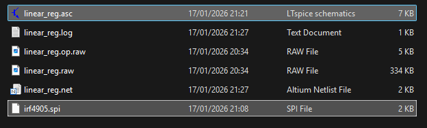
linear_reg.asc 17/01/2026 21:21 LTspice schematics 7 KB linear_reg.log 17/01/2026 21:27 Text Document 1 KB linear_reg.op.raw 17/01/2026 20:34 RAW File 5 KB linear_reg.raw 17/01/2026 20:34 RAW File 334 KB linear_reg.net 17/01/2026 21:27 Altium Netlist File 2 KB irf4905.spi 17/01/2026 21:
in „LTSpice Model IRF4905“ · Analoge Elektronik und Schaltungstechnik · · Screenshots
-
Datei
lcdcon_ft245.asm
Endadresse bei der Bildausgabe in X Richtung .def temp =r16 .def temp2 =r17 .def temp3 =r18 .def NextOp =r19 ;Zähler für Parameter eines Befehls .def Flags =r20 ;Allgemeine Bits .def XAdresseLow=r26 ;Writepointer Spalte .def ZeileL =r27 ;Writepointer Zeile LSB .def AdresseLow =r28 ;Readpointer Spalte .
in „LCD Controller für 640x480 LCD mit mega8515“ · Projekte & Code ·
-
Datei
lcdcon_ft245.asm
Endadresse bei der Bildausgabe in X Richtung .def temp =r16 .def temp2 =r17 .def temp3 =r18 .def NextOp =r19 ;Zähler für Parameter eines Befehls .def Flags =r20 ;Allgemeine Bits .def XAdresseLow=r26 ;Writepointer Spalte .def ZeileL =r27 ;Writepointer Zeile LSB .def AdresseLow =r28 ;Readpointer Spalte .
in „LCD Controller für 640x480 LCD mit mega8515“ · Projekte & Code ·
-
Datei
lcdcon_ft245_4bit.asm
Endadresse bei der Bildausgabe in X Richtung .def temp =r16 .def temp2 =r17 .def temp3 =r18 .def NextOp =r19 ;Zähler für Parameter eines Befehls .def Flags =r20 ;Allgemeine Bits .def XAdresseLow=r26 ;Writepointer Spalte .def ZeileL =r27 ;Writepointer Zeile LSB .def AdresseLow =r28 ;Readpointer Spalte .
in „LCD Controller für 640x480 LCD mit mega8515“ · Projekte & Code ·
-
Datei
lcdcon_ft245_4bit.asm
ja, dann ist nächster Wert ein Befehl -> NextOp.Escape setzen. ret ;*** Bearbeitung der Daten *** Daten: cpi NextOp, 0 ;Paramter oder Daten ? brne Next sbrc Flags, ZeileH ;Pixel in der oberen oder unteren Displayhälfte ? rjmp untereHalfte obereHalfte
in „LCD Controller für 640x480 LCD mit mega8515“ · Projekte & Code ·
-
Datei
lcdcon_ft245_4bit320.asm
ja, dann ist nächster Wert ein Befehl -> NextOp.Escape setzen. ret ;*** Bearbeitung der Daten *** Daten: cpi NextOp, 0 ;Paramter oder Daten ? brne Next st X+,temp cpi XAdresseLow, XMax ;Spalten Adresse > Max ? brlo normal clr XAdresseLow ;Spalten
in „LCD Controller für 640x480 LCD mit mega8515“ · Projekte & Code ·
-
Datei
lcdcon_ft245_4bit320.asm
ja, dann ist nächster Wert ein Befehl -> NextOp.Escape setzen. ret ;*** Bearbeitung der Daten *** Daten: cpi NextOp, 0 ;Paramter oder Daten ? brne Next sbi portd, XSCL ld temp2, X ;Lader Wert aus SRAM andi temp2, 15 ;obere Datenhälfte der SRAM Daten
in „LCD Controller für 640x480 LCD mit mega8515“ · Projekte & Code ·
-
PDF
19230ds.pdf
and -5V supplies to power the converter, 1 - VCO Gain = LSBs per second per volt pins 23, 24, 26 and 27 must be no connection. Connect the 1.25 R VC VCO two VDD pins together to +5 VDC. Connect the two V SS pins where: Cs = 10 pF together to -5 VDC. Fs = 67 kHz when R CLK = 30 kΩ C VCO = 50 pF TABLE 2.
in „Stimulierung des Resolvers RD-19230“ · Mikrocontroller und Digitale Elektronik ·