warming up. − Flashing light indicates that the preselected temperature has been C reached. Note Please refer to the accessories section on page 18 for a list of tools P that can be connected to the WD 1 (M) / WD 1000 (M). U H K S L S E E V L L 8-18 WD 1 (M) / WD 1000 (M) 6 Operating the device 6.1 Setting
commutation (4Q) or very high commutation (3Q, Snubberless™) capability • BTA series UL1557 certified (file ref: 81734) G G • Packages are RoHS (2002/95/EC) compliant A12 A1A2 • Insulated tab (BTA series, rated at 2500 V ) RMS TO-220AB TO-220AB Ins. A2 Applications • Snubberless versions (BTA/BTB...W and T1635
mir aber schon öfter in Youtube Videos aufgefallen: https://www.amazon.de/gp/product/B0GF24BQV6/ref=ox_sc_saved_title_10? Nutze ich selbst schon seit längerem: https://www.akkuteile.de/ladegeraete/zubehoer-und-ersatzteile/yr-1035-professionelle-innenwiderstand-tester-fuer-akkus-bis-100-volt_
I(DD) Z 5 mA 2º.5 24.5 26.5 V Control Function Section (FB Pin) Internal Error Amplifier (EA) VFB=REF 1.°7 º.0 º.02 V Reference Input Short Load Protection (SLP) VFB=SLP 0.7 V Threshold Short Load Protection (SLP) TFB=Short 10 ms Debounce Time Demagnetization Comparator VFB=DEM º5 mV Threshold Minimum
1. Refer to the taping drawing. Seiko Instruments Inc. 3 BATTERY PROTECTION IC FOR 2-SERIAL-CELL PACK S-8242A Series Rev.3.0 _00 2. Product Name List (1) SOT-23-6W Table 1 Overcharge Overcharge Overdischarge
hole dimensions) (Terminal dimensions) The other terminal is also available upon request. Please refer page 328 for schematic of dimensions. Frequency coefficient of rated ripple current Frequency (Hz) 50 60 120 300 1k 10k 50k or more 16 to 100V 0.88 0.90 1.00 1.07 1.15 1.15 1.15 Coeff. 160 to 250V
E000 to E7FFH 11101 E800 to EFFFH 11110 F000 to F7FFH 11111 F800 to FFFFH (Example 1) Offset register 02H Character code 80H Character generator RAM start address 0001 0100 0000 0000 1 4 0 0 H (Example 2) The relationship between display RAM data and display characters γ and ζ are displayed by character
two output leads, measured in mm. against overvoltage with de- electrodes. Avago supports partial Refer to Figure 4. vices such as diverters, filters, discharge measurements per IEC/ capacitors, etc. EN/DIN EN 60747-5-2, a technique ComparativeTrackingIndex(CTI) II Energy consuming equipment developed
/w key. This value can be output to a printer, depending on the code setting selected. Output of “wRef” and “nRef” Code Changes No output 7 6 1 Reference sample quantity “nRef” 7 6 2 Average piece weight “wRef” 7 6 3 Piece count “nRef” and piece weight “wRef7 6 4 * Output of Net-/Tare-/Gross Weights/
supply cable - terminal panel 00357898-01 3 Power supply grounding cable - terminal panel 00324358-02 4 Power supply cable - terminal panel 00321113-02 5 Power supply cable - terminal panel 00356733-01 65 3 Power Supply Service Manual S-27 HM 3.2 Power supply unit 10/2005 US Issue 3.2.2 Standard version
tent DMA Acknowledge assertion during memory refresh periods. If DACK is asserted when REF is ac RCVCCO Receive Collision Count Overflow JAB Jabber tive, DACK assertion is ignored. REF is monitored to eliminate a bus arbitration problem observed on some MISS Missed Frame ISA platforms. MERR
been Stresses exceeding those listed in the Maximum Ratings table may damageDISCONTINUED. Please refer to the table on page 2 device. If any of these limits are exceeded, device functionality should not be assumed, damage may occur and reliability may be affected. Semiconductor Components Industries
4 8 0 6 0 7 E 3 0 0 F 0 2 4 4 1PIN INDEX 20 64 1 19 1.0TYP 0.4±0.1 0.15±0.05 φ0.20 M 0-10° 0.1 18.0REF 1.2±0.2 22.3±0.4 Unit:mm 14 Rev 1.2 LQFP64 C D 48 33 H G I 49 3 F A B E 64 17 K 1 16 J Symbol Dimensions in mm Min. Nom. Max. A 8.90 9.00 9.10 B 6.90 7.00 7.10 C 8.90 9.00 9.10 D 6.90 7.00 7.10 E
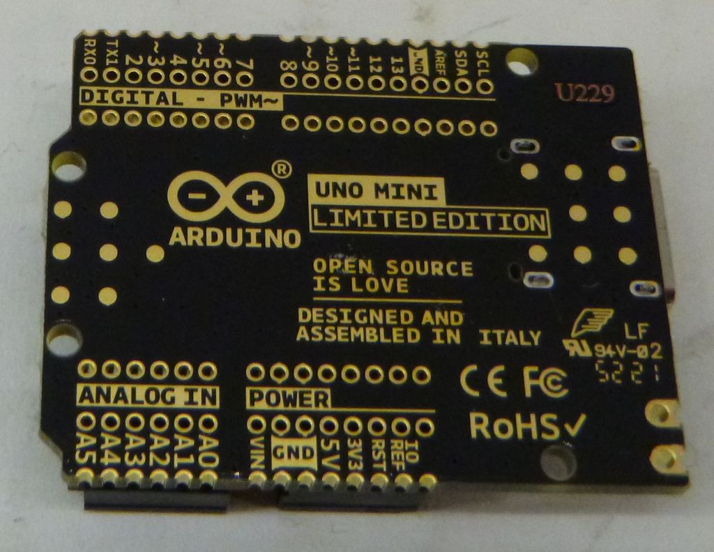
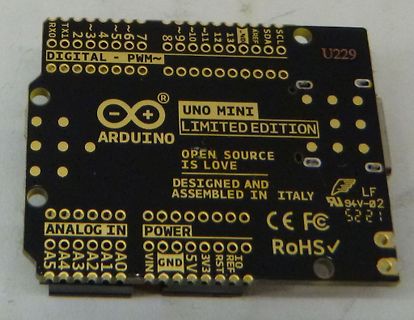
U229, ARDUINO, UNO MINI LIMITED EDITION, OPEN SOURCE IS LOVE, DESIGNED AND ASSEMBLED IN ITALY, LF 94V-02, 5221, ANALOG IN, POWER, CE, FC, RoHS, 0A5, 0A4, 0A3, 0A2, 0A1, 0A0, VIN, GND, 5V, 3V3, RST, REF, IO
Ursprünglichen Fühler t_ref von der Heizungssteuerung abklemmen, 3 Fühler t_1, t_2, t_fb vom gleichen Typ kaufen und mit Wärmeleitkleber an einen Zementwiderstand R_heiz kleben. 2 von den angeklebten Fühlern t_1, t_2 kann man
einer kleinen Schaltung wird R_heiz so beheizt oder mit Lüfter gekühlt, dass t_fb denselben Wert wie t_ref hat, fertig! ;)
1 L 51 GES 95 52 29R 5 5 3 61 GES 06 42 19R R R L 81 GES 26 22 38R k7. 4 05R 2 91 GES 36 12 1TNI L 02 GES6 02 18R k7. 4 15R 0 1 2 3 4 5 6 7 8 9 L 1 2 3 4 5 6 7 1 1 1 1 1 1 1 1 1 1 2 2 2M M M MS N U0 1 2 S E LT B A E E EC C C C VX XK K K T E HI e S S S R 0 1 5 d - - 5 5 W n H H C C S a W W m 8 C 2 042
& 2, EEPROM, ADC, PWM 1 & 2, I/O ports peripherals and Power Bridge) occurs, causing its wake-up. Refer to Figure 12 below. Figure 13. Wait mode flow chart WAIT INSTRUCTION OSCILLATOR ON PERIPH. CLOCK ON CPU CLOCK OFF I-BIT CLEARED N RESET N INTERRUPT Y Y OSCILLATOR ON PERIPH. CLOCK ON CPU CLOCK ON I-BIT
REFERENCES EUROPEAN VERSION IEC JEDEC JEITA PROJECTION ISSUE DATE 99-12-27 SOT96-1 076E03 MS-012 03-02-18 2004 Jan 13 17 Philips Semiconductors Product specification LIN transceiver TJA1020 SOLDERING To overcome these problems the double-wave soldering method was specifically developed. Introduction to
your convenience, we have included brief descriptions of the major tools in this document. Please refer to figure 1 to get an overview about the typical data flow involved with a MEGATEXT PLUS or MEGATEXT advanced on screen display software development. The individual tool combination may vary. DEDITOR
may also impact roaming performance. For more information about Turbo Roaming parameter settings, refer to the product manual.fic load. 2. DFS (Dynamic Frequency Selection) channel support: In AP mode, when a radar signal is detected, the device will automatically switch to another channel. However,
may also impact roaming performance. For more information about Turbo Roaming parameter settings, refer to the product manual. 2. DFS (Dynamic Frequency Selection) channel support: In AP mode, when a radar signal is detected, the device will automatically switch to another channel. However, according
tested in Orcad’s PSPICE 10.0 which is equivalent to in a number of different simulators. Please refer to your simulator software reference manual on how to create Cadence PSPICE 15.x. The type of modeling a schematic symbol and relating a netlist to the symbol. technique that was used to model the
24 C1 101230 1C 01 R 13 D 9 1 1121R 5 L 2 8 C10023 C 3011R 900 CI 51 R 6 D 702C R 3 C1 R R 0R 5 1 02 809R 6021D 7 L 9 40 3 1234 C 2 9 0 0 10 1R 101 2 C 10 B 549C 4 3021D 9 C 2 2 4 C 82 R 01 R S 2 4021D C C C 702R 9 1 6 1R 02 R U 449C 1 R 012C L C 9 91 1R 2 819R 0021CI 5021D 619C C R R10 3 349C 2121R
90E7 JMP DIS 0 8 NOP 0F91 0 8 NOP 0F1 A BYTE 0F52 S 2 0F92 9 C B F JNZ S 2 TAB: table of C 4 0 2 LDI 02 0 F 1 B 3F 0F55 0F96 C 8 1 F ST MIN 7-segment 8 F 0 1 S 301 0F94 0 8 NOP 0 F 1 C 06 0F98 0 8 NOP 0 F 1 D 5B 0F579 8 F 0 0 DLY 00* 0F99 0 8 NOP OF I E 4F 3 F XPPC 3 0 F 1 F 66 C 4 0 6 LDI 06 0 F 2 0 6D
and commercial applications where low power and low voltage operation are essential. The AT24C01A/02/04/08/16 is available in space saving 8-pin PDIP, AT24C02 (AT24C01A/02 /0 4/08 /1 6), 8-Pin MSOP (AT24C01A/02), 8-Pin TSSOP (AT24C01A/02/04/08/16), and 8-Pin and 14-Pin JEDEC SOIC (AT24C01A/02/04/08/
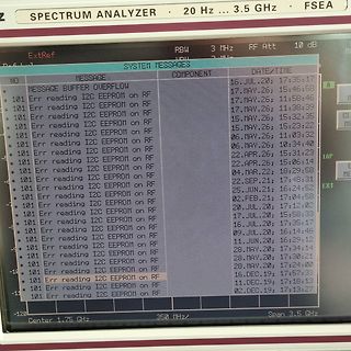
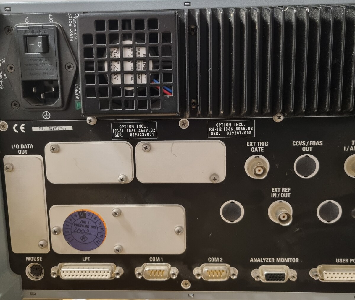
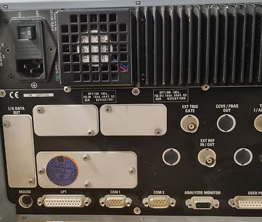
F1/F2: EC127 TR 0.1H 240V SUPPLY OPTION INCL. FSE-BH 1066.466.02 SER. 629433/001 OPTION INCL. FSE-812 1066.5065.02 SER. 029267/005 CE SER. 028977/036 I/O DATA OUT EXT TRIG GATE CCVS/FBAS OUT EXT REF IN/OUT MOUSE LPT COM 1 COM 2 ANALYZER MONITOR USER PC PRÜFUNG BIS
COM0A1)|(0<<COM0A0)|(1<<COM0B1)|(0<<COM0B0)|(1<<WGM01)|(1<<WGM00) ;TCCR0A out TCCR0A, AL ldi AL, (0<<WGM02)|(0<<CS02)|(0<<CS01)|(1<<CS00) ;TCCR0B /1 out TCCR0B, AL clr AL ;kein INT sts TIMSK0, AL ; Counter 2 Mode 3 ldi AL, (1<<COM2A1)|(0<<COM2A0)|(1<<COM2B1)|(0<<COM2B0)|(1<<WGM21)|(1<<WGM20) ;TCCR2A sts TCCR2A
SLVS036F – SEPTEMBER 1981 – REVISED AUGUST 2000 functional block diagram VI IN Error – Amplifier VO[ V ref1 ) R2Ǔ R1 + V O OUT Protection Circuit V ref R1 ADJ R2 absolute maximum ratings over operating temperature range (unless otherwise noted) † Input-to-output differential voltage, l – O . . . . . . .
J-Datenlogger-Thermoelement-Thermometer-4-Kanal-Anzeige-Echtzeit-Datenprotokollierung-ADJ-Kompensation-J-Thermoelement/dp/B0CBRKS253/ref=pd_aw_subss_hxwPER_sspa_mw_detail_m_sccl_1_5/257-7017322-8735002 also Display ausbauen und getrennt von der Elektronik hinter deine Blende. Ein speziell für dich gebautes ist unrealistisch .
1 L 51 GES 95 52 29R 5 5 3 61 GES 06 42 19R R R L 81 GES 26 22 38R k7. 4 05R 2 91 GES 36 12 1TNI L 02 GES6 02 18R k7. 4 15R 0 1 2 3 4 5 6 7 8 9 L 1 2 3 4 5 6 7 1 1 1 1 1 1 1 1 1 1 2 2 2M M M MS N U0 1 2 S E LT B A E E EC C C C VX XK K K T E HI e S S S R 0 1 5 d - - 5 5 W n H H C C S a W W m 8 C 2 042
CC, TA=25˚C 9.0 16 mA DC POWER SUPPLY CC Supply Current (Includes fCLK= 640 kHz, Ladder Current) V REF/2 NC, T A=25˚C = and CS 5V ADC0801/02/03/04LCJ/05 1.1 1.8 mA ADC0804LCN/LCWM 1.9 2.5 mA Note 1: Absolute Maximum Ratings indicate limits beyond which damage to the device may occur. DC and AC electrical

 Bild
Bild
 Bild
Bild
 Bild
Bild
 Bild
Bild
 Bild
Bild
 Bild
Bild
 Bild
Bild