-
Datei
sid.c
); // CTC mode 4 TCCR1B |=(1<<CS10); // no prescaling OCR1A=9; // 1mhz clock @ 20mhz F_CPU SET_CS; sid_reset(); sid_clear(); return; } void sid(void) { sid_init(); sid_reset(); sid_write(24, 0x0f); sid_write(1, 0x06); sid_write(5, 12); sid_write(6,4); sid_write(4,33); for(;;) { locate(0,0); printf("$%02x $%02x $%02x", sid_read(25), sid_read(26), sid_read(27)); sid_write(1, sid_read(25)); } return; // never reached! }
in „mos6581 SID (C64 Soundchip) für AVR“ · Projekte & Code ·
-
Datei
sid.lst
AVRASM ver. 2.1.42 C:\Dokumente und Einstellungen\inet\Eigene Dateien\sid\main.asm Sun May 03 21:49:28 2015 C:\Dokumente und Einstellungen\inet\Eigene Dateien\sid\main.asm(2): Including file 'C:\Dokumente und Einstellungen\inet\Eigene Dateien\sid\m162def.inc' C:\Dokumente
in „Suche jemanden zum compileren“ · Mikrocontroller und Digitale Elektronik ·
-
Bild
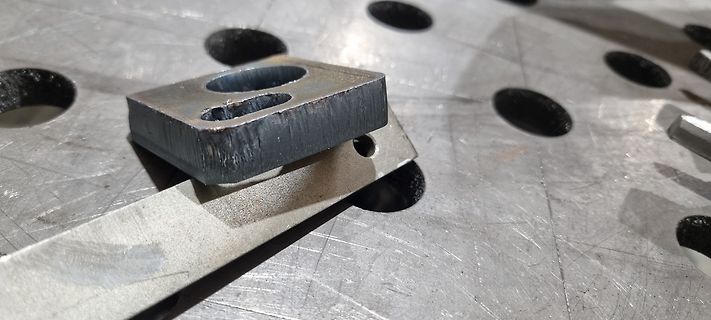
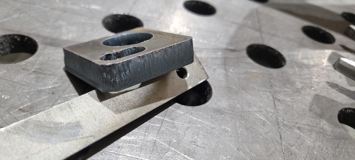
Metallblock auf Lochplatte
side.jpg
in „Prima Power Domino - 4kW CO2 Laser - Schnittbild“ · Mechanik, Gehäuse, Werkzeug · · Fotos
-
Bild
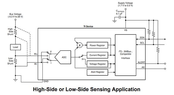
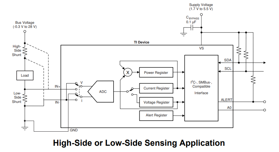
Blockschaltbild einer High-Side oder Low-Side Sensing Anwendung
Bus Voltage (-0.3 V to 28 V) High-Side Shunt Load Low-Side Shunt IN+ IN- TI Device V ADC X Power Register SDA SCL Current Register I2C-, SMBus-, Compatible Interface Voltage Register ALERT A0 Alert Register VS CBYPASS 0.1 µF GND High-Side or Low-Side Sensing Application
in „Neue Bauteile: Hitzeresistente Leuchtdioden, I3C-Sensoren und vieles andere mehr“ · Analoge Elektronik und Schaltungstechnik · · Diagramme
-
Bild
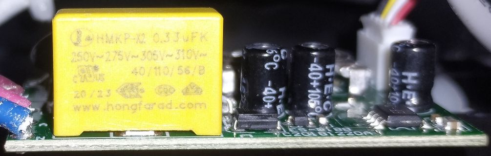
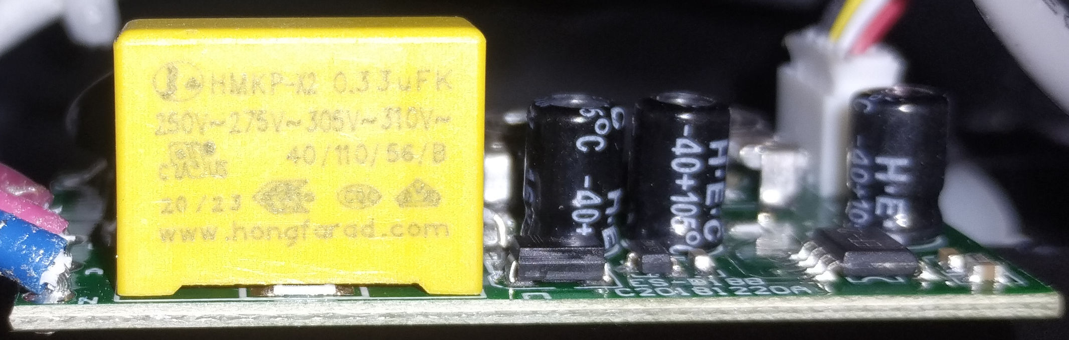
Nahaufnahme einer Leiterplatte mit gelbem Kondensator und Elektrolytkondensatoren
HMKP-X2 0.33uF 250V~ 275V~ 305V~ 310V~ 40/110/56/B 20/23 www.hongfarad.com H:E C -40+105C H:E C -40+85 ES-8188 C20161220A
in „Lampe mit Bewegungsmelder geht nicht mehr aus“ · Haus & Smart Home · · Platinenfotos
-
PDF
SIDE_sheet.pdf
9 8 3 3 IC3C + 0 1 0 6 4 4 2 C 1 C 1 C 1 C D +C5 V C1 V C2 V C3 V C4 G IC2P IC1P IC3P IC4P CF-IF (SIDE) für Z180-Stamp 10µ N 100n N 100n N 100n N 100n 1 G 8 G 7 G 7 G TITLE: SIDE D G Document Number: REV: A Date: 27.05.2016 10:47 Sheet: 1/1 27.05.2016 11:01 B:\Privat\AVRCPM\SVN_Mikro\trunk\stamp\SIDE\sheet\SIDE.sch (Sheet: 1/1)
in „Z180-Stamp Modul“ · Mikrocontroller und Digitale Elektronik ·
-
PDF
SIDE_TOP.pdf
1 U 1 3 ED R L SV1 4 2 1 27.05.2016 11:06 B:\Privat\AVRCPM\SVN_Mikro\trunk\stamp\SIDE\sheet\SIDE.brd
in „Z180-Stamp Modul“ · Mikrocontroller und Digitale Elektronik ·
-
PDF
SIDE_TOP.pdf
JP1 3 5 C I C C 3 C C I C I 1 D R L 1 2 3 6 5 4 S S S S S S SV1 4 C 0 2 2 1 4 I R R 2 1 $ U
in „Z180-Stamp Modul“ · Mikrocontroller und Digitale Elektronik ·
-
PDF
SIDE_sheet.pdf
74LV125 9 8 A2 VCC IC3C 1 2 C 1 C 1 C 1 C V V V V N + C5 C1 C2 C3 C4 G IC2P IC1P IC3P IC4P CF-IF (SIDE) für Z180-Stamp 10µ D 100n D 100n D 100n D 100n G G G G 1 8 7 7 TITLE: SIDE1 N G Document Number: REV: A Date: 31.05.2016 15:30 Sheet: 1/1
in „Z180-Stamp Modul“ · Mikrocontroller und Digitale Elektronik ·
-
Bild
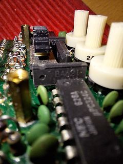
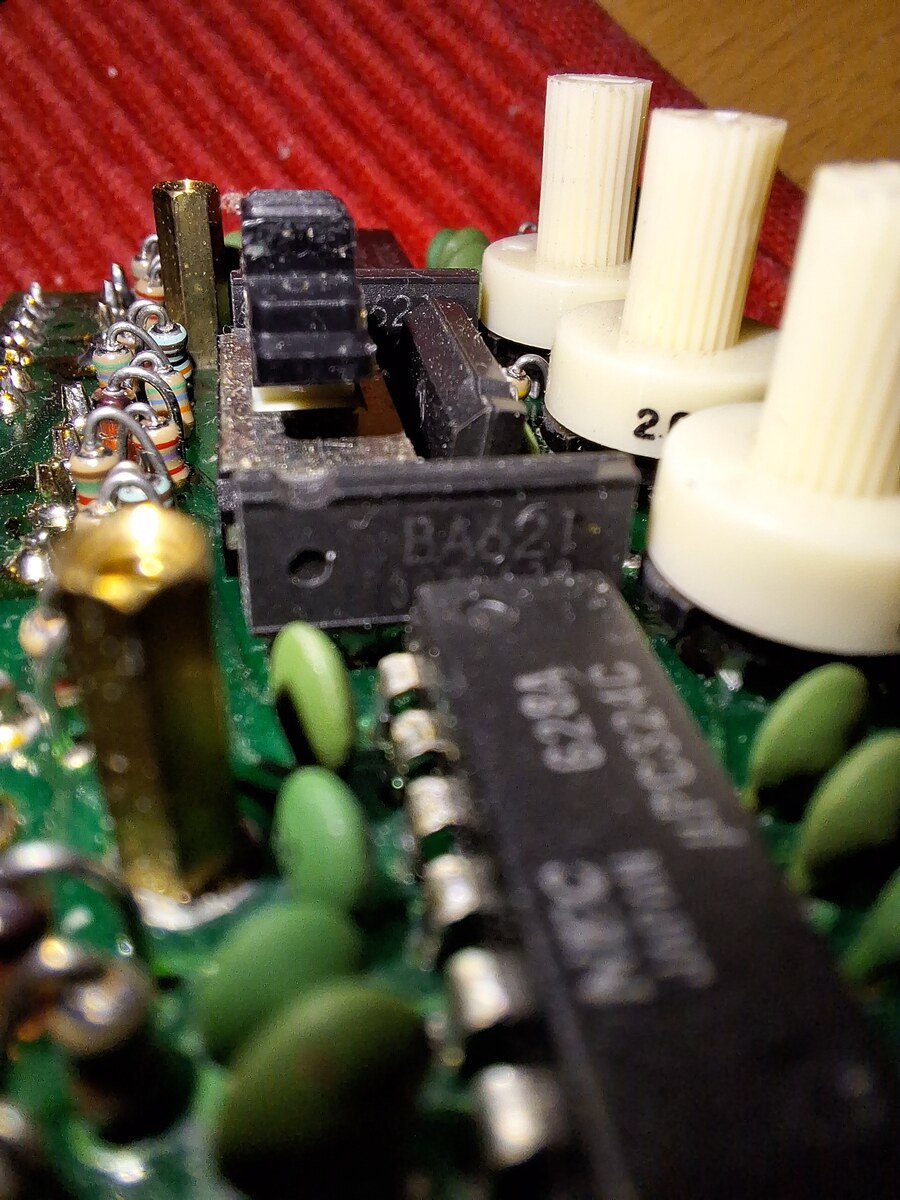
Nahaufnahme einer Leiterplatte mit integrierten Schaltkreisen
BA621 628A MPC324C JAPAN
in „Pinlayout des BA621 von Rohm“ · Analoge Elektronik und Schaltungstechnik · · Platinenfotos
-
Bild
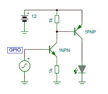
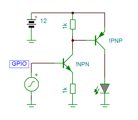
Schaltplan mit NPN- und PNP-Transistor zur LED-Ansteuerung
12, 1k, !PNP, !NPN, GPIO, 1k
in „Mit BC807 12v-LED schalten“ · Analoge Elektronik und Schaltungstechnik · · Schaltpläne
-
Bild
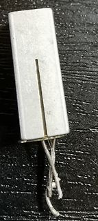
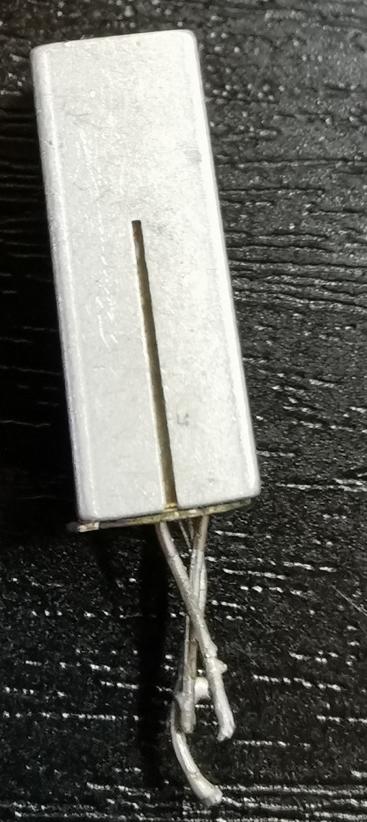
Metallgehäuse mit Drähten
AC178_side.jpg
in „Was ist besser - TDA2003 oder TBA810S“ · Analoge Elektronik und Schaltungstechnik · · Fotos
-
Bild
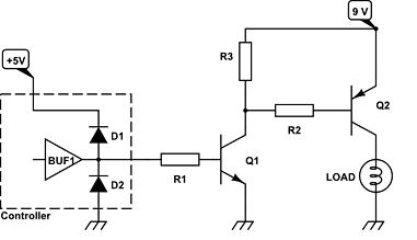
Schaltplan einer Transistor-Treiberstufe
+5V Controller BUF1 D1 D2 R1 Q1 R3 R2 Q2 9V LOAD
in „kleine Spannung (µC) größere Spannung (13V) Highside schalten. Bauteil?“ · Analoge Elektronik und Schaltungstechnik · · Schaltpläne
-
Bild
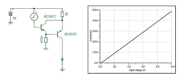
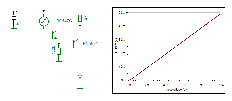
Schaltplan und Strom-Spannungs-Kennlinie
24 BC547C 2k 470k BC557C 5.0m 4.0m 3.0m 2.0m 1.0m 0.0 Current (A) 0.0 2.0 4.0 6.0 8.0 10.0 Input voltage (V)
in „V-Ref und verstärker IC gesucht/ Komplementär-TL431“ · Analoge Elektronik und Schaltungstechnik · · Screenshots
-
PDF
High-Side-Switch.pdf
FET_IRLMS6802DBF T300 UIN S J306 UIN LED1 1 D9 6 3 G 3 n IO-SW ON GND 1 k 3 0 J305 2 5 R 1 C 1 VIN VOUT F +5V 4 F 3 4 5 n LOW -> Ausgeschaltet GND_P 8 0 VIN VOUT C 0 HIGH -> Eingeschaltet GND_P C 1 FPF1005 1 R315 T302 IO-SW GND_P1 GND_P1 4k7 T_BC817_NPN GND_P Datum Name Bearb. <undefined> <DRAWN> <undefined> Gepr. <TITLE> Norm. 1 1 <COMPANY> Zust. Aenderung Datum Name Datei Name: (Ers.fuer:) (Ers.durch:)
in „FET schaltet Baugruppe AN/AUS“ · Analoge Elektronik und Schaltungstechnik ·
-
PDF
High-Side-Switch.pdf
FET_IRLMS6802DBF T300 UIN S J306 UIN LED1 1 D9 6 3 G 3 n IO-SW ON GND 1 k 3 0 J305 2 5 R 1 C 1 VIN VOUT F +5V 4 F 3 4 5 n LOW -> Ausgeschaltet GND_P 8 0 VIN VOUT C 0 HIGH -> Eingeschaltet GND_P C 1 FPF1005 1 R315 T302 IO-SW GND_P1 GND_P1 4k7 T_BC817_NPN GND_P Datum Name Bearb. <undefined> <DRAWN> <undefined> Gepr. <TITLE> Norm. 1 1 <COMPANY> Zust. Aenderung Datum Name Datei Name: (Ers.fuer:) (Ers.durch:)
in „P-Kanal MOSFET mit 3.3V schalten?“ · Analoge Elektronik und Schaltungstechnik ·
-
PDF
-
Bild
Meme über SIDS und Impfungen
SIDS IS ACTUALLY VACCINE INDUCED DEATH @jabbingmesoftly
in „Funkgerät als Babyfon?“ · HF, Funk und Felder · · Sonstiges
-
Datei
Programm.txt.txt
= 0 LCDClock(); // SID = 0 P5OUT &= 0xFB; // --> 0 LCDClock(); // SID = 0 D4 LCDClock(); // SID = 0 D5 LCDClock(); // SID = 0 D6 LCDClock(); // SID = 0 D7 P5OUT &= 0xFB; // --> 0 LCDClock(); // SID = 0 LCDClock(); // SID
in „LCD Display Seriell Ansteuern“ · Mikrocontroller und Digitale Elektronik ·
-
PDF
CY8C4147AZI.pdf
SID63 R PULLUP Pull-up resistor 3.5 5.6 8.5 – kΩ SID64 R PULLDOWN Pull-down resistor 3.5 5.6 8.5 – Input leakage current (absolute SID65 IIL – – 2 nA 25 °C, DDD = 3.0 V value) SID66 C Input capacitance
-
Datei
i2c_mos6581.c
#include <avr/io.h> #include "i2c_mos6581.h" #include "i2cmaster.h" #define SID_WRITE sid_clr_rw() #define SID_READ sid_set_rw() // all static inlined functions are for internal use only static inline void sid_set_rw(void); static inline void sid_clr_rw(void); static inline void
in „mos6581 SID (C64 Soundchip) für AVR“ · Projekte & Code ·
-
PDF
ADUM1250_1251-Datasheet.pdf
to-Side 2, Falling Edge 3 tPHL12 162 275 ns 4 Side 2-to-Side 1, Rising Edge tPLH21 31 70 ns Side 2-to-Side 1, Falling Edge 5 tPHL21 85 155 ns 3V Operation 3.0V ≤V DD1V DD2≤ 3.6V, C L1C = L2pF, R1 = 1.0 kΩ, R2 = 120 Ω 2 Side 1-to-Side 2, Rising Edge tPLH12 82 125 ns Side 1-to-Side 2, Falling Edge 3 tPHL12 196 340 ns 4 Side 2-to-Side 1, Rising Edge tPLH21 32 75 ns Side 2-to-Side 1, Falling Edge 5 tPHL21 110 210 ns PULSEWIDTH
in „I2C nach Stop conition Hänger!“ · Mikrocontroller und Digitale Elektronik ·
-
PDF
igbt_driver_Tipps.pdf
8 Low Side Off PGND RG1_off ParS1 RSense 0.1 D01IN1182 13/23 AN1299 APPLICATION NOTE HIGH SIDE OFF-LOW SIDE TURNED ON Figure 14. The Low side is turned On, the current that flows through the low side switch is
in „Induktion - Problem bei Resonanz“ · Analoge Elektronik und Schaltungstechnik ·
-
PDF
PCA9517_Level_Shifter_I2C.pdf
and the external pull-up resistor pulls the pin HIGH. When the B-side falls first and goes below 0.3V CCB the A-side driver is turned on and the A-side pulls down to 0 V. The B-side pull-down is not enabled unless the B-side voltage goes below 0.4 V. If the B-side low voltage does not go below 0.5 V, the A-side driver will turn off when the B-side voltage is above 0.7V . If the B-side low CCB voltage goes below 0.4 V, the B-side pull-down driver is enabled and the B-side will only PCA9517_3 © NXP B.V. 2007
in „I2C Taktsignal“ · Mikrocontroller und Digitale Elektronik ·
-
Datei
c64.asm
; C64 includes ; SID SID_FREQLO1 = $D400 SID_FREQHI1 = $D401 SID_PWLO1 = $D402 SID_PWLHI1 = $D403 SID_CR1 = $D404 SID_AD1 = $D405 SID_SR1 = $D406 SID_FREQLO2 = $D407 SID_FREQHI2 = $D408 SID_PWLO2 = $D409 SID_PWLHI2 = $D40A SID_CR2 = $D40B SID_AD2 = $D40C SID_SR2 = $D40D SID_FREQLO3 = $D40E SID_FREQHI3 = $D40F SID_PWLO3 = $D410 SID_PWLHI3 = $D411 SID_CR3 = $D412 SID_AD3 = $D413 SID_SR3 = $D414 SID_FCLO = $D415 SID_FCHI = $
in „Wettkampf Opa(MOS6502) gegen Frischling(ATmega)“ · Mikrocontroller und Digitale Elektronik ·
-
PDF
NCP51530-D-1324764-1.pdf
DFN10 (Top View) (Top View) Table 1. PIN DESCRIPTION SOIC 8 PACKAGE Pin Out Name Function 1 HIN High side input 2 LIN Low side input 3 GND Ground reference 4 LO Low side output 5 VCC Low side and logic supply 6 HB High side supply return 7 HO High side output 8 VB High side voltage supply Table 2. PIN DESCRIPTION DFN10 PACKAGE Pin Out Name Function 1 VCC Low side and logic supply 2 HIN High side input 3 LIN Low side input 4 GND Ground reference 5 GND Ground reference 6 LO Low side output 7 NC No Connect 8 HB High side supply return 9 HO High side output 10 VB
in „Hilfe bei Halbbrückenschaltung benötigt“ · Analoge Elektronik und Schaltungstechnik ·
-
PDF
Atmel-9251-ATA6836C-ATA6838C-Open-Load-Detection_Application-Note.pdf
a high-side open-load at the dedicated low-side output register (LSx) for the associated output (OUTx). Figure 1-3. High-side Load Configuration VS VS HSx OUTx LSx GND If LSx = 1, then the high-side load is open
in „Keine Open Load Meldung bei ata6836c und IFX9201SG!“ · Mikrocontroller und Digitale Elektronik ·
-
PDF
Microsemi_13.56_MHz__Class-D_Half_Bridge.pdf
destruction of Q1 and Q2. To reduce this effect we must reduce the stray capacitance in the high Side Transformer T1 to the minimum and also install a Common Mode Choke on the primary side of the transformer. See Figure 2. Common Mode T1 Choke High Side Control Control Input High Side Common Pin 16
in „Bauplan für HF Netzteil gesucht.“ · HF, Funk und Felder ·
-
PDF
MAX3816A.pdf
75 side, DD for display side) Supply Threshold used to detect low-to- Cable high transition relative to supplyide 12.5 % of Low-to-High Threshold VTRIGIL (VCC for cable side,DD for Display 17.5 Supply display
in „[S] Extender für HDMI über CAT5e (1080p@60Hz)“ · Markt ·
-
Datei
pads.py
0], left[1], pads_per_side)) res.extend(pad_line(bot[0], bot[1], pads_per_side)) res.extend(pad_line(right[0], right[1], pads_per_side)) res.extend(pad_line(top[0], top[1], pads_per_side)) elif sides == 2: left = ((-pad_row_distance / 2.0, pads_side_length / 2.0), (-pad_row_distance / 2.0, -pads_side_length / 2.0)) right =((pad_row_distance / 2.0, -pads_side_length / 2.0), (pad_row_distance / 2.0, pads_side_length / 2.0)) res.extend(pad_line(left
-
Datei
TestTerminal5b.py
() when closing window # Rahmen1 Rahmen1 = Frame(Mainwindow, background = "#002040") Rahmen1.pack(side = TOP, fill = X) #Rahmen2 Rahmen2 = Frame(Mainwindow, background = "#002040") Rahmen2.pack(side = TOP, fill = X) #Rahmen3 Rahmen3 = Frame (Mainwindow, background = "#002040") Rahmen3.pack(side = TOP, fill = X) #Rahmen4 Rahmen4 = Frame (Mainwindow, background = "#002040") Rahmen4.pack(side = TOP, fill = X) #Rahmen5 Rahmen5 = Frame (Mainwindow, background = "#002040") Rahmen5.pack(side = TOP, fill = X) #Rahmen6 Rahmen6 = Frame (Mainwindow, background = "#002040") Rahmen6.pack(side = TOP
in „Python3 und PySerial: Diverse Probleme“ · Softwareentwicklung ·
-
PDF
FD6287T_fortiorEnglish.pdf
ratings (unless otherwise specified, all pins are referenced to COM). parameter symbol scope unit High-side floating absolute voltage -0.3ÿ275 In VB1,2,3 High-side floating offset voltage, VS1,2,3 VB1,2,3-25ÿVB1,2,3+0.3 In high-side output voltage, VHO1,2,3 VS1,2,3-0.3ÿVB1,2,3+0.3 In low-side supply voltage
in „hc-160a s2 Datenblatt?“ · Mikrocontroller und Digitale Elektronik ·
-
PDF
Vollbr_cke_VNH3SP30.pdf
A Status of High-Side and Low-Side Switches A; Open Drain Output 8 PWM PWM Input 9 NC Not connected EN /DIAG 10 B B Status of High-Side and Low-Side Switches B; Open Drain Output 11 INB Counter Clockwise Input OUT B,Heat 15, 16, 21 Slug3 Source of High-Side Switch B / Drain of Low-Side Switch B 26, 27, 28 GND A Source of Low-Side Switch A (*) 18, 19, 20 GND Source of Low-Side Switch B (*) B (*) Note: GAD and GBD must be externally connected together 2/
in „VNH3SP30 auch als Halbbrücke“ · Mikrocontroller und Digitale Elektronik ·
-
PDF
vnh2sp30.pdf
Protect the High Side and the Low Side switches from the high voltage on VOLTAGE the battery line in all configuration for the motor. HIGH SIDE AND LOW SIDE DRIVER Drive the gate of the concerned switch to allow a propDS
in „25A Regler per PWM“ · Mikrocontroller und Digitale Elektronik ·
-
PDF
Si823x_-_AMP_ISOdriver.pdf
Overlap Programmable Inputs Peak Output Protection Dead Time Current (A) Si8230 High-Side/Low-Side VIA, VIB 0.5 Si8231 High-Side/Low-Side PWM 0.5 Si8232/7 Dual Driver — — VIA, VIB 0.5 Si8233 High-Side/Low-Side VIA, VIB 4.0 Si8234 High-Side/Low-Side PWM 4.0 Si8235/6/8 Dual
in „Si8223 - Highside/Lowside Treiber - normales Verhalten?“ · Mikrocontroller und Digitale Elektronik ·
-
PDF
bts780gp_Quadswitch_Driver.pdf
high-side switches and power supply voltage Heat-Slug 2 or Heat-Dissipator 10 GH2 Gate of high-side switch 2 11 ST2 Status of high-side switch 2; open Drain output 12 SH2 Source of high-side switch 2 13, 14 SL2 Source of low-side switch 2 15 GL2 Gate of low-side switch 2 16 DL2 Drain of low-side switch 2 Heat-Slug 3 or Heat-Dissipator 18 DL1 Drain of low-side switch 1 Heat-Slug 1 or Heat-Dissipator Bold type: Pin needs power
in „moderne H-Bridge gesucht“ · Mikrocontroller und Digitale Elektronik ·
-
PDF
sidtech3.pdf
write data into the selected SID register. This pin is normally connected to the system Read/ Write line. CS (Pin 8) This TTL-level input is a low active chip select which controls data transfers between SID and the microprocessor.
in „MOS6581/Commodore SID Timing?“ · Mikrocontroller und Digitale Elektronik ·
-
PDF
IX2113-UG-1548297.pdf
of a high voltage gate driver configured as a half-bridge driver. The IX2113 has independent high-side and low-side referenced output channels, both of which are capable of sourcing and sinking 2A peak current. The floating high-side channel can drive MOSFETs or IGBTs up to 600V from the common reference
in „H-Brücke funktioniert nur mit Tastkopf“ · Mikrocontroller und Digitale Elektronik ·
-
PDF
BTS780.pdf
high-side switches and power supply voltage Heat-Slug 2 or Heat-Dissipator 10 GH2 Gate of high-side switch 2 11 ST2 Status of high-side switch 2; open Drain output 12 SH2 Source of high-side switch 2 13, 14 SL2 Source of low-side switch 2 15 GL2 Gate of low-side switch 2 16 DL2 Drain of low-side switch 2 Heat-Slug 3 or Heat-Dissipator 18 DL1 Drain of low-side switch 1 Heat-Slug 1 or Heat-Dissipator Bold type: Pin needs power
in „BTS780GP Motortreiber“ · Analoge Elektronik und Schaltungstechnik ·
-
PDF
IRS2092.pdf
V CLAMPL Low side zener diode clamp voltage 19.6 20.4 21.6 V ICC5 mA High Side Floating Supply UV BS+ High side well UVLO positive threshold 8.0 8.5 9.0 UV BS- High side well UVLO negative threshold 7.8 8.3 8.8 V UV
in „Car Hifi Endstufe kein Ton, axton D500 digital, Irs2092s Vorverstärker“ · Analoge Elektronik und Schaltungstechnik ·
-
PDF
C906560.pdf
Thermistor 17 NU Low−side Emitter Connection − Phase U 18 NV Low−side Emitter Connection − Phase V 19 NW Low−side Emitter Connection − Phase W 20 W Phase W Output / High−side Floating Supply Offset Voltage 22 VBW High−side Floating Supply Voltage − Phase W 26 V Phase V Output / High−side Floating Supply Offset Voltage 28 VBV High−side Floating Supply Voltage − Phase V 32 U Phase U Output / High−side Floating Supply Offset Voltage 34 VBU High−side Floating Supply Voltage − Phase U 38
in „Ersatz für ON-Semi STK5Q4U362J-E / STK5Q4U363J-E bzw. passt da NFAQ1060L33T / NFAQ1060L36T“ · Analoge Elektronik und Schaltungstechnik ·
-
Datei
log.txt
, session[0], sid=b3f8a1da 92eb0866 Mon Jan 6 09:29:57 2020 us=872122 xxx.xxx.xxx.xxx:57577 TLS: received control channel packet s#=0 sid=b3f8a1da 92eb0866 Mon Jan 6 09:29:57 2020 us=872136 xxx.xxx.xxx.xxx:57577 ACK
in „Openvpn Server Umzug Client kann sich nicht verbinden“ · PC Hard- und Software ·
-
PDF
FD6287T_cn-translated.pdf
Unless otherwise specified, all pins areCOMas a reference point) parameter symbol scope unit High side floating absolute voltage V B1,2,3 - 0.3~275 V High Side Floating Offset Voltage V S1,2,3 V B1,2-25~V B1,2+0.3 V High side output voltage VHO1,2,3 V S1,-0.3~V B1,2+0.3 V Low side supply voltage V CC
in „PWM: Motortreiber schaltet bei Tastverhältnis Reduktion ab“ · Analoge Elektronik und Schaltungstechnik ·
-
PDF
drv8350f_7_.pdf
to the high-side power MOSFET source. SLA 8 8 I Low-side source sense input. Connect to the low-side power MOSFET source. SLB 9 9 I Low-side source sense input. Connect to the low-side power MOSFET source. SLC 16 16
in „BLDC-Motor: Überspannung beim Bremsen trotz Durchschaltung aller Low-Side-MOSFETs?“ · Analoge Elektronik und Schaltungstechnik ·
-
Bild
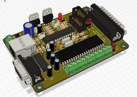
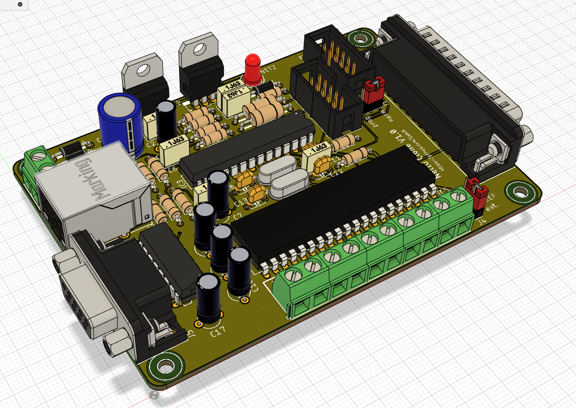
3D-CAD-Modell einer Leiterplatte mit elektronischen Bauteilen
Marking, NETZ, J63, J64, J65, J66, J67, J68, J69, J70, J71, J72, J73, J74, J75, J76, J77, J78, J79, J80, J81, J82, J83, J84, J85, J86, J87, J88, J89, J90, J91, J92, J93, J94, J95, J96, J97, J98, J99, J100, J101, J102, J103, J104, J105, J106, J107, J108, J109, J110, J111, J112, J113, J114, J115, J116, J117, J118, J119, J120, J121, J122, J123, J124, J125, J126, J127, J128, J129, J130, J131, J132, J133, J134, J135, J136, J137, J138, J139, J140, J141, J142, J143, J144, J145, J146, J147, J148, J149, J150, J151, J152, J153, J154, J155, J156, J157, J158, J159, J160, J161, J162, J163, J164, J165, J166
in „Pollin NetIO Hardware-Nachbau“ · Projekte & Code · · Layouts
-
Bild
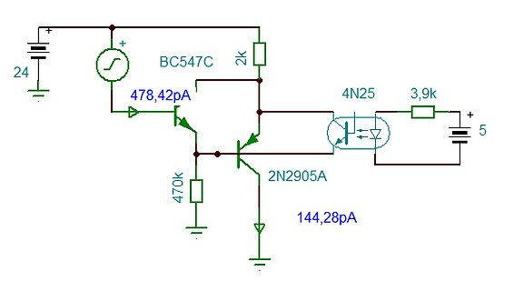
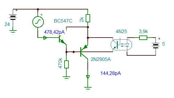
Schaltplan mit Transistoren und Optokoppler
24, +, BC547C, 478,42pA, 2k, 4N25, 3,9k, +, 5, 2N2905A, 144,28pA, 470k
in „V-Ref und verstärker IC gesucht/ Komplementär-TL431“ · Analoge Elektronik und Schaltungstechnik · · Schaltpläne
-
Bild
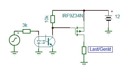
Schaltplan mit Optokoppler und MOSFET-Treiber
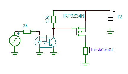
3k 10k IRF9Z34N 12 Last/Gerät
in „12V 2A per Raspberry Pi (3,3V) schalten“ · Analoge Elektronik und Schaltungstechnik · · Schaltpläne
-
Bild
Offene Elektronikplatine mit Seeed Studio Modul
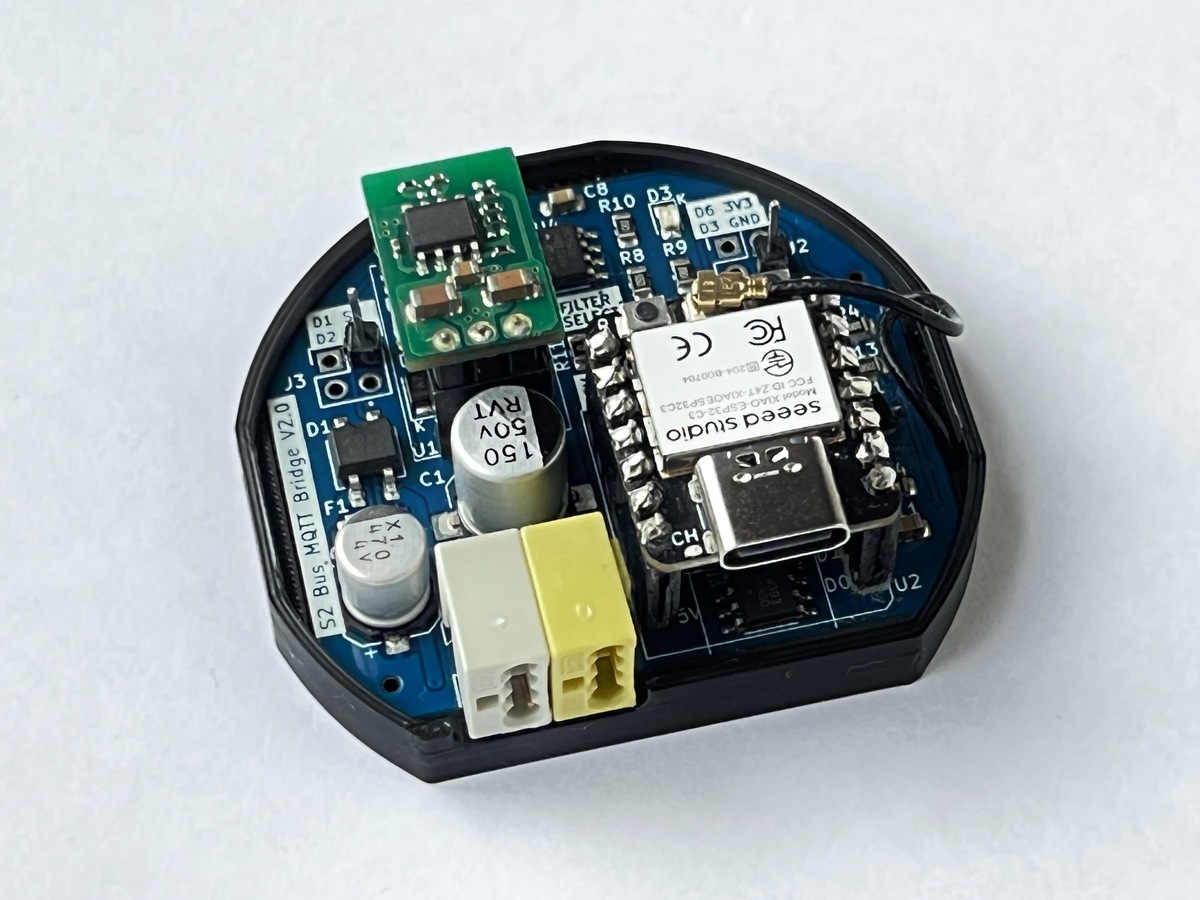
S2 Bus MQTT Bridge V2.0, C8, R10, D6 3V3, D3 GND, R8, R9, F1, Seeed studio, Model XIAO ESP32-C3, FCC CE, 150 50V, RV1, C1, C2, D1, D2, F1, <, >
in „Comelit Videosprechanlage mit Raspberry Pi ansteuern“ · Haus & Smart Home · · Platinenfotos
-
PDF
BTS_100_High_Side.pdf
Smart Highside Power Switch BTS 100 TEMPFET Features ● P channel ● Enhancement mode ● Temperature sensor with thyristor characteristic ● The drain pin is electrically shorted to the tab Pin 1 2 3 G D S Type V DS ID R DS(on) Package Ordering Code BTS 100 — 50 V — 8 A 0.3 TO-220AB C67078-A5007-A2 Maximum Ratings Parameter Symbol Values Unit Drain-source voltage VDS — 50 V Drain-gate voltageRGS= 20 k VDGR — 50 Gate-source voltage VGS ± 20 Continuous drain currentC = 30 °C ID — 8.0 A ISO drain current I — 1.5 D-ISO TC = 85 ˚CV GS= 10 V,VDS = 0.5 V Pulsed drain current, T = 25 °C I — 32 C D puls Short

in „Motorsteuerung mit kollektorschaltung“ · Mikrocontroller und Digitale Elektronik ·
-
Datei
sid-sod-v2.asm
; V24 ueber SID - SOD ; V2 - 1200Bd ; ; 09.12.2018 ; SID-SODV2 ; ; Quelltext ueberarbeitet ; ; FCT SID-SOD aus MonitorV5.5 ; ; Warteschleife auf 1/2Bitzeit angepasst ; ; Buffer 9000h-9fffh ; TX wartet auf CTS=LOW gibt
in „Suche MOPPEL Projekt in Heft oder .PDF“ · Mikrocontroller und Digitale Elektronik ·