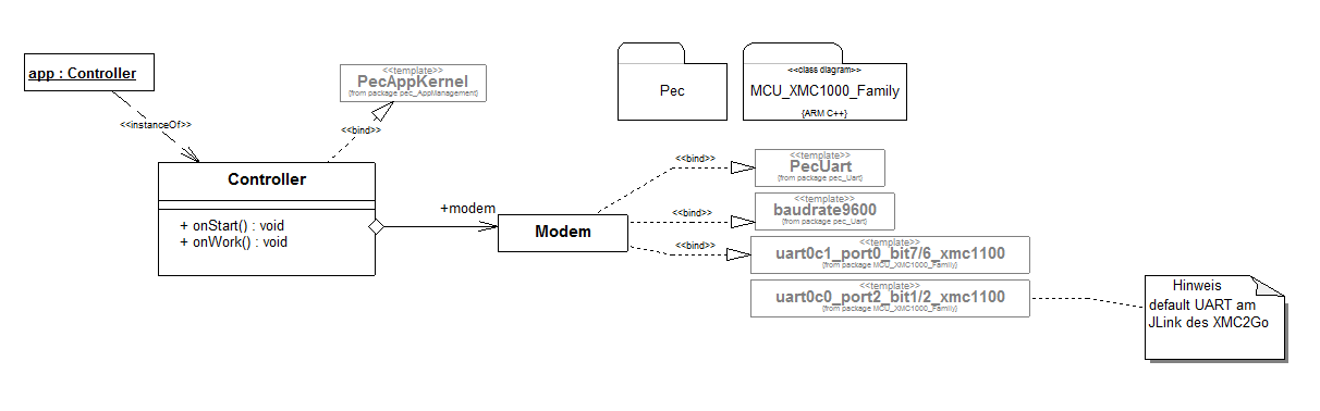
1 | //////////////////////////////////////////////////////
|
2 | //
|
3 | // Diese Quellcodedatei wurde automatisch erzeugt.
|
4 | // SiSy UML CodeGenerierung
|
5 | //
|
6 | //////////////////////////////////////////////////////
|
7 | #define GeneratedBySisy
|
8 | #define cpp_Modem
|
9 | #define SISY_CLASS_NAME Modem
|
10 | #include "Modem.h"
|
11 | #include "Controller.h"
|
12 |
|
13 | #define uartNoTx_
|
14 | #define uartNoRx_
|
15 | #define _TheUsic USIC0_CH1
|
16 | extern Controller* pGlob_app;
|
17 | #define app (*pGlob_app)
|
18 |
|
19 | /////////////////////////////
|
20 | Modem::Modem()
|
21 | {
|
22 | // aus Template: PecUart
|
23 | // init
|
24 | init();
|
25 | // config
|
26 | #define noBaudrate9600
|
27 | #ifndef noBaudrate
|
28 | config(9600);
|
29 | #endif
|
30 | }
|
31 | /////////////////////////////
|
32 | void Modem::config(uint32_t baudrate, uint8_t dataBits, UartParity parity, UartStopBits stopBits)
|
33 | {
|
34 | // aus Template: SysUartXmc GoToSiSy:o:953|zBase:1
|
35 | // Disable clock gating to USICn
|
36 | #if UC_FAMILY == XMC1
|
37 | //SCU_UnlockProtectedBits(); // only for 32 clocks
|
38 | SCU_GENERAL->PASSWD = 0x000000C0UL; // disable bit protection
|
39 |
|
40 | //SCU_CLK->CGATCLR0 |= SCU_CLK_CGATCLR0_USIC0_Msk;
|
41 | SCU_CLOCK_UngateClock( SCU_CLOCK_ID_USIC0 );
|
42 |
|
43 | //SCU_LockProtectedBits();
|
44 | SCU_GENERAL->PASSWD = 0x000000C3UL; // enable bit protection
|
45 | #endif
|
46 | // für XMC4
|
47 | #if UC_FAMILY == XMC4
|
48 | SCU_RESET_ClearResetRequest( SCU_RESET_REQUEST_SOURCE_USIC0 );
|
49 | #endif
|
50 |
|
51 | /* Enable the module kernel clock and the module functionality */
|
52 | _TheUsic->KSCFG |= USIC_CH_KSCFG_MODEN_Msk | USIC_CH_KSCFG_BPMODEN_Msk;
|
53 |
|
54 | ////// Baudrate //////
|
55 | uint32_t pdiv1 = 1023; // PDIV = Divider Mode: Divider Factor to Generate, max 10 bit
|
56 | uint32_t dctq1 = 16; // DCTQ = Denominator for Time Quanta Counter, max 5 bit
|
57 | uint32_t pctq1 = 1; // PCTQ = Pre-Divider for Time Quanta Counter, max 2 bit
|
58 | if(baudrate>100000)
|
59 | dctq1 = 4;
|
60 |
|
61 | uint32_t br1=0;
|
62 | while(pdiv1>2 && br1<baudrate)
|
63 | {
|
64 | pdiv1--;
|
65 | br1 = SystemCoreClock / (pdiv1*dctq1*pctq1);
|
66 | }
|
67 | uint32_t fdrStep; // FDR.STEP = Fractional Divider Register - Step Value, max 10 bit
|
68 | fdrStep = 1024*baudrate/br1;
|
69 |
|
70 | /* FDR.DM = 02b (Fractional divider mode) */
|
71 | uint32_t dm = 0x02; // Fractional divider mode selected
|
72 | if( br1==baudrate )
|
73 | {
|
74 | dm = 0x01; // Normal divider mode selected.
|
75 | fdrStep = 0x3FF;
|
76 | }
|
77 | WR_REG(_TheUsic->FDR, USIC_CH_FDR_DM_Msk, USIC_CH_FDR_DM_Pos, dm);
|
78 | WR_REG(_TheUsic->FDR, USIC_CH_FDR_STEP_Msk, USIC_CH_FDR_STEP_Pos, fdrStep);
|
79 |
|
80 | /* Configure baud rate generator */
|
81 | /* BAUDRATE = fCTQIN/(BRG.PCTQ x BRG.DCTQ) */
|
82 | /* CLKSEL = 0 (fPIN = fFD), CTQSEL = 00b (fCTQIN = fPDIV), PPPEN = 0 (fPPP=fPIN) */
|
83 | uint32_t brg = 0;
|
84 | brg |= (pdiv1-1)<<USIC_CH_BRG_PDIV_Pos;
|
85 | brg |= (dctq1-1)<<USIC_CH_BRG_DCTQ_Pos;
|
86 | brg |= (pctq1-1)<<USIC_CH_BRG_PCTQ_Pos;
|
87 | WR_REG(_TheUsic->BRG
|
88 | ,USIC_CH_BRG_PCTQ_Msk | USIC_CH_BRG_DCTQ_Msk | USIC_CH_BRG_PDIV_Msk | USIC_CH_BRG_CLKSEL_Msk | USIC_CH_BRG_PPPEN_Msk | USIC_CH_BRG_CTQSEL_Msk
|
89 | ,0
|
90 | ,brg
|
91 | );
|
92 |
|
93 |
|
94 |
|
95 | /* Configuration of USIC Shift Control */
|
96 | /* SCTR.FLE = 8 (Frame Length) */
|
97 | /* SCTR.WLE = 8 (Word Length) */
|
98 | /* SCTR.TRM = 1 (Transmission Mode) */
|
99 | /* SCTR.PDL = 1 (This bit defines the output level at the shift data output signal when no data is available for transmission) */
|
100 | _TheUsic->SCTR &= ~(USIC_CH_SCTR_TRM_Msk | USIC_CH_SCTR_PDL_Msk);
|
101 | _TheUsic->SCTR |= (0x01UL << USIC_CH_SCTR_PDL_Pos) | (0x01UL << USIC_CH_SCTR_TRM_Pos);
|
102 | // Databits
|
103 | WR_REG( _TheUsic->SCTR, USIC_CH_SCTR_FLE_Msk, USIC_CH_SCTR_FLE_Pos, (dataBits-1) );
|
104 | WR_REG( _TheUsic->SCTR, USIC_CH_SCTR_WLE_Msk, USIC_CH_SCTR_WLE_Pos, (dataBits-1) );
|
105 |
|
106 | /* Configuration of USIC Transmit Control/Status Register */
|
107 | /* TBUF.TDEN = 1 (TBUF Data Enable: A transmission of the data word in TBUF can be started if TDV = 1 */
|
108 | /* TBUF.TDSSM = 1 (Data Single Shot Mode: allow word-by-word data transmission which avoid sending the same data several times*/
|
109 | _TheUsic->TCSR &= ~(USIC_CH_TCSR_TDEN_Msk);
|
110 | _TheUsic->TCSR |= USIC_CH_TCSR_TDSSM_Msk | (0x01UL << USIC_CH_TCSR_TDEN_Pos);
|
111 |
|
112 | /* Configuration of Protocol Control Register */
|
113 | /* PCR.SMD = 1 (Sample Mode based on majority) */
|
114 | /* PCR.STPB = 0 (1x Stop bit) */
|
115 | /* PCR.SP = <dctq (Sample Point) */
|
116 | /* PCR.PL = 0 (Pulse Length is equal to the bit length) */
|
117 | _TheUsic->PCR &= ~(USIC_CH_PCR_ASCMode_SP_Msk | USIC_CH_PCR_ASCMode_PL_Msk);
|
118 | _TheUsic->PCR |= USIC_CH_PCR_ASCMode_SMD_Msk | ((dctq1/2) << USIC_CH_PCR_ASCMode_SP_Pos);
|
119 | // StopBits
|
120 | WR_REG(_TheUsic->PCR, USIC_CH_PCR_ASCMode_STPB_Msk, USIC_CH_PCR_ASCMode_STPB_Pos, stopBits);
|
121 |
|
122 | /* ----- Configure Transmit Buffer ----- */
|
123 | /* Standard transmit buffer event is enabled */
|
124 | /* Define start entry of Transmit Data FIFO buffer DPTR = 0*/
|
125 | _TheUsic->TBCTR &= ~(USIC_CH_TBCTR_SIZE_Msk | USIC_CH_TBCTR_DPTR_Msk);
|
126 |
|
127 | /* Set Transmit Data Buffer to 64 */
|
128 | _TheUsic->TBCTR |= 0x06UL << USIC_CH_TBCTR_SIZE_Pos;
|
129 |
|
130 | /* Configure Receive Buffer */
|
131 | /* Standard receive buffer event is enabled */
|
132 | /* Define start entry of Receive Data FIFO buffer DPTR = 0*/
|
133 | _TheUsic->RBCTR &= ~(USIC_CH_RBCTR_SIZE_Msk | USIC_CH_RBCTR_DPTR_Msk);
|
134 |
|
135 | /* Set Receive Data Buffer to 64 */
|
136 | _TheUsic->RBCTR |= 0x06UL << USIC_CH_RBCTR_SIZE_Pos;
|
137 |
|
138 | /* ----- Initialize UART_RX (DX0) -----*/
|
139 | /* Pin as input */
|
140 | {
|
141 | SysGpio gpio;
|
142 | gpio.init(PORT0, BIT6);
|
143 | gpio.setMode(PCx_Input);
|
144 | }
|
145 | /* Select Pin as input for USIC */
|
146 | WR_REG( _TheUsic->DX0CR, USIC_CH_DX0CR_DSEL_Msk, USIC_CH_DX0CR_DSEL_Pos, UsicSelDXnC);
|
147 |
|
148 | /* ----- Initialize UART_TX (DOUT) -----*/
|
149 | /* Pin as output controlled by ALT7 = U0C1.DOUT0 */
|
150 | {
|
151 | SysGpio gpio;
|
152 | gpio.init(PORT0, BIT7);
|
153 | gpio.setMode(PCx_AF7);
|
154 | }
|
155 |
|
156 | /* Configuration of Channel Control Register */
|
157 | /* CCR.PM = 00 ( Disable parity generation) */
|
158 | /* CCR.MODE = 2 (ASC mode enabled. Note: 0 (USIC channel is disabled)) */
|
159 |
|
160 | // Parity
|
161 | WR_REG( _TheUsic->CCR, USIC_CH_CCR_PM_Msk, USIC_CH_CCR_PM_Pos, parity );
|
162 | // Uart-Mode
|
163 | WR_REG( _TheUsic->CCR, USIC_CH_CCR_MODE_Msk, USIC_CH_CCR_MODE_Pos, 0x02UL );
|
164 |
|
165 | // GoToSiSy:d:2477|o:2488|zbase:132
|
166 |
|
167 | }
|