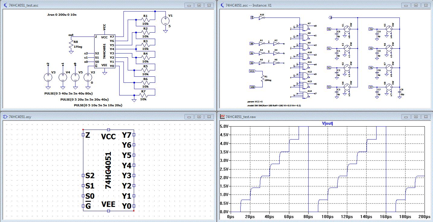
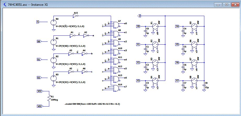
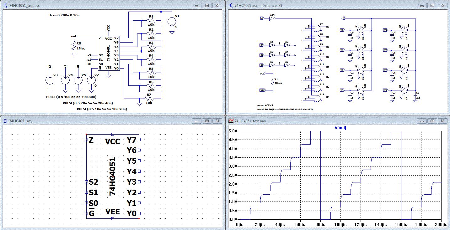
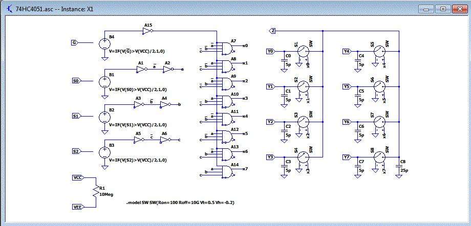
1 | .SUBCKT 74HC4051 VCC VEE GND INH A2 A1 A0 Y0 Y1 Y2 Y3 Y4 Y5 Y7 Y7 Z
|
2 | ********************************************************************************
|
3 | *Node VCC +Vsupply
|
4 | *Node VEE -Vsupply
|
5 | *Node GND Ground
|
6 | *Node INH Inhibit
|
7 | *Node A2-A0 A2-A0 Control Inputs
|
8 | *Node Y0-Y7 Mux Input/Output 1 - Mux Input/Output 8
|
9 | *Node Z Common Input/Output
|
10 | *******************************************************************************
|
11 | **** Convert Analog Control Input to Digital ***
|
12 | aADCInh [INH] [INHd] AtoD
|
13 | aADC2 [A2] [A2d] AtoD
|
14 | aADC1 [A1] [A1d] AtoD
|
15 | aADC0 [A0] [A0d] AtoD
|
16 | ****Decode Digital Input*********
|
17 | aDEC [INHd A2d A1d A0d] [Control1d Control2d Control3d Control4d Control5d Control6d Control7d Control8D] MUXDIGDEC
|
18 |
|
19 | ***Convert Digital Control Signals to Analog control voltages ***
|
20 | aDAC1 [Control1d] [Control1] DtoA
|
21 | aDAC2 [Control2d] [Control2] DtoA
|
22 | aDAC3 [Control3d] [Control3] DtoA
|
23 | aDAC4 [Control4d] [Control4] DtoA
|
24 | aDAC5 [Control5d] [Control5] DtoA
|
25 | aDAC6 [Control6d] [Control6] DtoA
|
26 | aDAC7 [Control7d] [Control7] DtoA
|
27 | aDAC8 [Control8d] [Control8] DtoA
|
28 | **** Mux Input Select Switches ****
|
29 | aSW1 Control1 ( Y0 Z ) MC74HC4051
|
30 | aSW2 Control2 ( Y1 Z ) MC74HC4051
|
31 | aSW3 Control3 ( Y2 Z ) MC74HC4051
|
32 | aSW4 Control4 ( Y3 Z ) MC74HC4051
|
33 | aSW5 Control5 ( Y4 Z ) MC74HC4051
|
34 | aSW6 Control6 ( Y5 Z ) MC74HC4051
|
35 | aSW7 Control7 ( Y6 Z ) MC74HC4051
|
36 | aSW8 Control8 ( Y7 Z ) MC74HC4051
|
37 | *** Diode Protection ***
|
38 | *D1 VCC Y0 D_Protect
|
39 | *D2 Y0 VEE D_Protect
|
40 | *D3 VCC Y1 D_Protect
|
41 | *D4 Y1 VEE D_Protect
|
42 | *D5 VCC Y2 D_Protect
|
43 | *D6 Y2 VEE D_Protect
|
44 | *D7 VCC Y3 D_Protect
|
45 | *D8 Y3 VEE D_Protect
|
46 | *D9 VCC Y4 D_Protect
|
47 | *D10 Y4 VEE D_Protect
|
48 | *D11 VCC Y5 D_Protect
|
49 | *D12 Y5 VEE D_Protect
|
50 | *D13 VCC Y6 D_Protect
|
51 | *D14 Y6 VEE D_Protect
|
52 | *D15 VCC Y7 D_Protect
|
53 | *D16 Y7 VEE D_Protect
|
54 | *D17 VCC Z D_Protect
|
55 | *D18 Z VEE D_Protect
|
56 | .MODEL MUXDIGDEC d_chip ( behaviour= "
|
57 | +/inputs INH A2 A1 A0
|
58 | +/outputs D1 D2 D3 D4 D5 D6 D7 D8
|
59 | +/table 9
|
60 | +; CONTROL IN DATA OUT
|
61 | +;INH A2 A1 A0 1 2 3 4 5 6 7 8
|
62 | + L L L L H L L L L L L L
|
63 | + L L L H L H L L L L L L
|
64 | + L L H L L L H L L L L L
|
65 | + L L H H L L L H L L L L
|
66 | + L H L L L L L L H L L L
|
67 | + L H L H L L L L L H L L
|
68 | + L H H L L L L L L L H L
|
69 | + L H H H L L L L L L L H
|
70 | + H X X X L L L L L L L L
|
71 | +")
|
72 | .MODEL D_Protect D()
|
73 | .MODEL AtoD adc_bridge (in_low= 0.8 in_high = 3.8)
|
74 | .MODEL DtoA dac_bridge (out_low= 0.0 out_high= 5.0)
|
75 | .MODEL MC74HC4051 aswitch (cntl_off= 0.5 cntl_on= 3.5
|
76 | + r_off= 1e7 r_on= 80 log=TRUE )
|
77 | .ENDS 74HC4051
|