von
Daniel S (Gast)
25.12.2014 16:24
Hallo,
Ich bin wirklich am verzweifeln, möchte mit 2 RFM70 Modulen eine
Funkübertragung starten, aktuell nur mit Testbytes.
Der eine Atmega8L (Extern 8 Mhz) ist der Sender, der sendet im Abstand
von 1 sek, die Bytes 0x01,0x02,0x03. Der Sender Signalisiert mir durch
eine LED das gesendet wurde, diese Blinkt auch im 1 Sek. Takt.
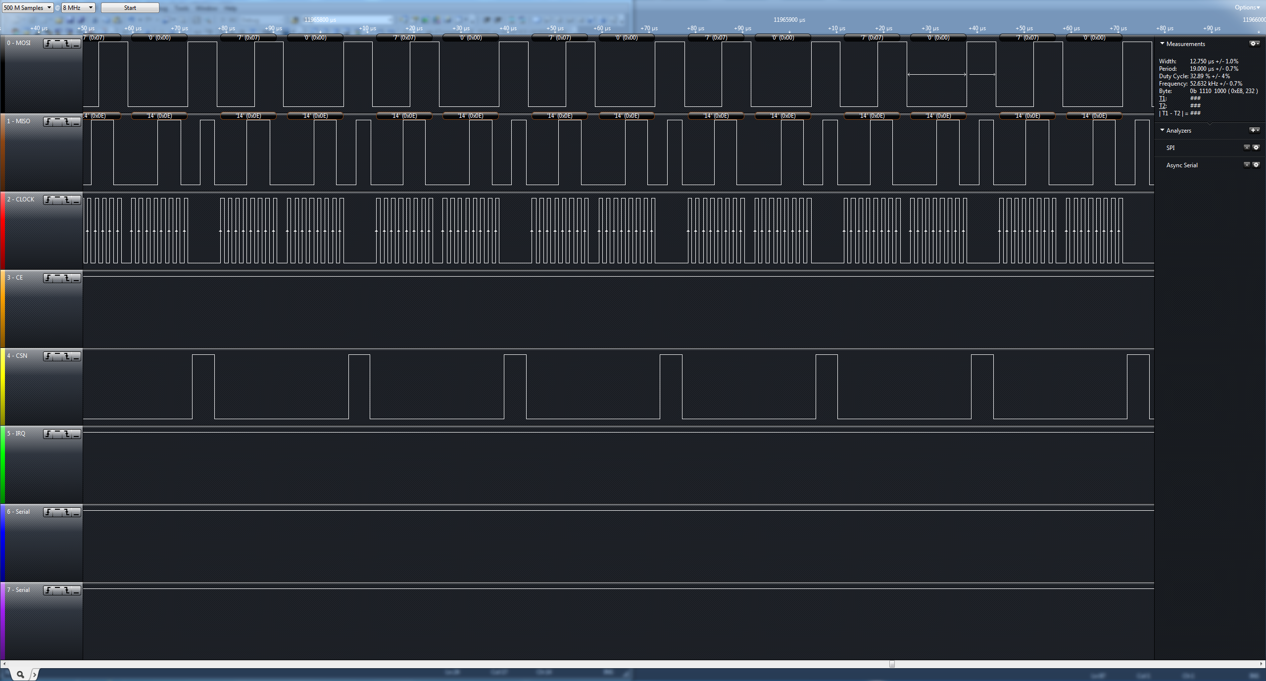
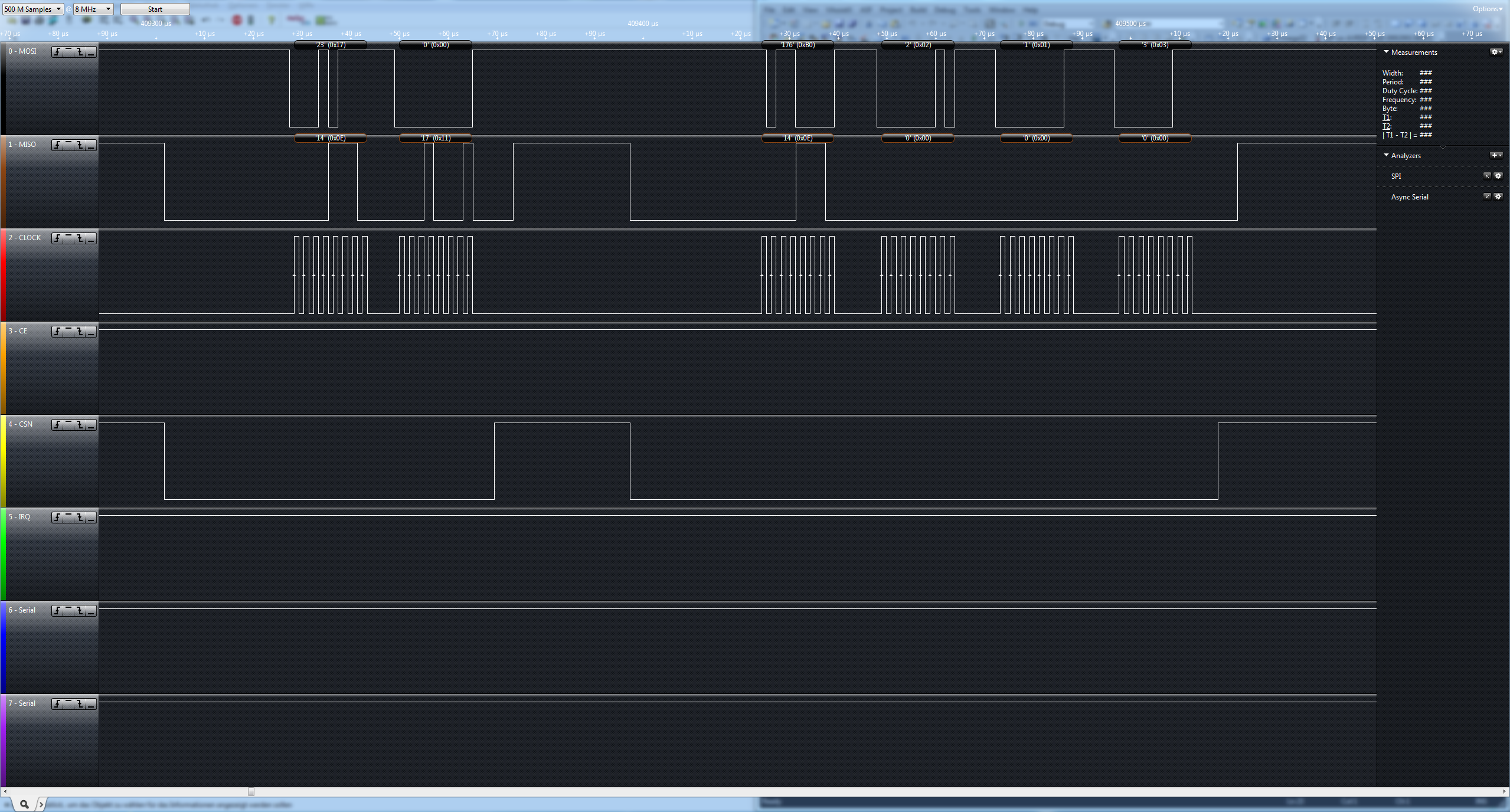
Im Anhang findet Ihr die SPI Kommunikation des Modules beim Senden, die
ChipID wurde korrekt erkannt und es wird auch gesendet.
der AtMega16 (Extern 10 Mhz) ist der Empfänger (VCC=5V,VDD
Funkmodul=3.3V), hier läuft ebenfalls die Kommunikation, aber egal wer
sendet oder empfängt, es tut sich nichts, der IRQ Pin bleibt beim
Empfänger auch auf High.
Habe schon auf einen Atmega8L Empfänger auf 3.3v basis das ganze
getestet, nur habe ich hier das selbige Problem (Wollte ein evtl. 5V
Pegel Problem am Empfänger ausschließen)
Ich habe nun mittlerweile 8 RFM70 Module ausprobiert, aber es läuft
einfach nicht. Den Code den ich nutze ist von Daniel Weber
(http://projects.weber-itam.de/rfm70-funkmodul/ )
Vielleicht kann mal jemand drüber schauen, ich bin die letzten 7 tage
nur noch am verzweifeln.... Verdrahtet ist alles korrekt. Die Module
habe ich auch schon X mal getauscht... ich bin ratlos!
Der Sender hat folgenden Code
rfm70.c / sender 1 /*
2 Diese Library bassiert auf der Arduino RFM70 Library, ich habe sie lediglich so
3 angepasst, dass man sie auf einem AVR und ohne zusätzliche Libs von Arduino
4 verwenden kann.
5
6 Es sind nur die wichtigstens Funktionen implementiert!
7 Bei Fragen oder Anregungen:
8 Mein Blog: http:://projects.web4clans.com
9 Meine Email: daniel.weber@web4clans.com
10
11 */
12
13 #include "rfm70.h"
14 #include "../inventory.h"
15 ///////////////////////////////////////////////////////////////////////////////
16 // Register initialization values and command macros //
17 ///////////////////////////////////////////////////////////////////////////////
18
19 //************ Address definition commands
20 const uint8_t PROGMEM RFM70_cmd_adrTX [] = { ( 0x20 | 0x10 ), 0x34 , 0x43 , 0x10 , 0x10 , 0x01 };
21 const uint8_t PROGMEM RFM70_cmd_adrRX0 [] = { ( 0x20 | 0x0A ), 0x34 , 0x43 , 0x10 , 0x10 , 0x01 };
22
23 //************ Bank0 register initialization commands
24 const uint8_t PROGMEM RFM70_bank0Init [][ 2 ] = {
25 // address data
26 { ( 0x20 | 0x00 ), 0x08 }, //Disable CRC ,CRC=1byte, POWER UP, TX
27 { ( 0x20 | 0x01 ), 0x3F }, //Enable auto acknowledgement data pipe0-5
28 { ( 0x20 | 0x02 ), 0x3F }, //Enable RX Addresses pipe0-5
29 { ( 0x20 | 0x03 ), 0x03 }, //RX/TX address field width 5byte
30 { ( 0x20 | 0x04 ), 0xff }, //x = 250 ms = 4000ms, y = 15 tries
31 { ( 0x20 | 0x05 ), 0x17 }, //channel = 0x17
32 { ( 0x20 | 0x06 ), 0x17 }, //air data rate-2M,out power 5dbm,setup LNA gain high (0dBM)
33 { ( 0x20 | 0x07 ), 0x07 }, //
34 { ( 0x20 | 0x08 ), 0x00 }, //
35 { ( 0x20 | 0x09 ), 0x00 }, //
36 { ( 0x20 | 0x0C ), 0xc3 }, //LSB Addr pipe 2
37 { ( 0x20 | 0x0D ), 0xc4 }, //LSB Addr pipe 3
38 { ( 0x20 | 0x0E ), 0xc5 }, //LSB Addr pipe 4
39 { ( 0x20 | 0x0F ), 0xc6 }, //LSB Addr pipe 5
40 { ( 0x20 | 0x11 ), 0x20 }, //Payload len pipe0
41 { ( 0x20 | 0x12 ), 0x20 }, //Payload len pipe0
42 { ( 0x20 | 0x13 ), 0x20 }, //Payload len pipe0
43 { ( 0x20 | 0x14 ), 0x20 }, //Payload len pipe0
44 { ( 0x20 | 0x15 ), 0x20 }, //Payload len pipe0
45 { ( 0x20 | 0x16 ), 0x20 }, //Payload len pipe0
46 { ( 0x20 | 0x17 ), 0x00 }, // FIFO?
47 { ( 0x20 | 0x1C ), 0x3F }, //Enable dynamic payload legth data pipe0-5
48 { ( 0x20 | 0x1D ), 0x06 } //Enables Dynamic Payload Length,Enables Payload with ACK
49 };
50
51 //************ Bank1 register initialization commands
52 const uint8_t PROGMEM RFM70_bank1Init [][ 5 ] = {
53 // address data
54 { ( 0x20 | 0x00 ), 0x40 , 0x4B , 0x01 , 0xE2 },
55 { ( 0x20 | 0x01 ), 0xC0 , 0x4B , 0x00 , 0x00 },
56 { ( 0x20 | 0x02 ), 0xD0 , 0xFC , 0x8C , 0x02 },
57 { ( 0x20 | 0x03 ), 0x99 , 0x00 , 0x39 , 0x41 },
58 { ( 0x20 | 0x04 ), 0xb9 , 0x9E , 0x86 , 0x0B }, // b9? f9?
59 { ( 0x20 | 0x05 ), 0x24 , 0x06 , 0x7F , 0xA6 },
60 { ( 0x20 | 0x06 ), 0x00 , 0x00 , 0x00 , 0x00 },
61 { ( 0x20 | 0x07 ), 0x00 , 0x00 , 0x00 , 0x00 },
62 { ( 0x20 | 0x08 ), 0x00 , 0x00 , 0x00 , 0x00 },
63 { ( 0x20 | 0x09 ), 0x00 , 0x00 , 0x00 , 0x00 },
64 { ( 0x20 | 0x0a ), 0x00 , 0x00 , 0x00 , 0x00 },
65 { ( 0x20 | 0x0b ), 0x00 , 0x00 , 0x00 , 0x00 },
66 { ( 0x20 | 0x0C ), 0x00 , 0x12 , 0x73 , 0x00 },
67 { ( 0x20 | 0x0D ), 0x36 , 0xb4 , 0x80 , 0x00 }
68 };
69
70 //************ Bank1 register 14 initialization commands
71 const uint8_t RFM70_bank1R0EInit [] = {
72 // address Data...
73 ( 0x20 | 0x0E ), 0x41 , 0x20 , 0x08 , 0x04 , 0x81 , 0x20 , 0xCF , 0xF7 , 0xFE , 0xFF , 0xFF
74 };
75
76
77 //************ other commands: { <command>, <data>, ... }
78 const uint8_t PROGMEM RFM70_cmd_switch_cfg [] = { 0x50 , 0x53 }; // switch Register Bank
79 const uint8_t PROGMEM RFM70_cmd_flush_rx [] = { 0xe2 , 0x00 }; // flush RX FIFO
80 const uint8_t PROGMEM RFM70_cmd_flush_tx [] = { 0xe1 , 0x00 }; // flush TX FIFO
81 const uint8_t PROGMEM RFM70_cmd_activate [] = { 0x50 , 0x73 }; // Activation command
82 const uint8_t PROGMEM RFM70_cmd_tog1 [] = { ( 0x20 | 0x04 ), 0xd9 | 0x06 , 0x9e , 0x86 , 0x0b }; //assosciated with set1[4]!
83 const uint8_t PROGMEM RFM70_cmd_tog2 [] = { ( 0x20 | 0x04 ), 0xd9 & ~ 0x06 , 0x9e , 0x86 , 0x0b }; //assosciated with set1[4]!
84
85
86
87 void initSPI ( uint8_t clk_div )
88 {
89 // set the pin direction to output
90 DDR_SPI |= ( 1 << SCK ) | ( 1 << MOSI ) | ( 1 << CSN );
91
92 // chip select to high
93 PORT_SPI |= ( 1 << CSN );
94 // other to low
95 PORT_SPI &=~ (( 1 << MOSI ) | ( 1 << SCK ));
96
97 // init SPI
98 SPCR = ( 1 << SPE ) | ( 1 << MSTR );
99
100 // det clock divider
101 spiSetClockDivider ( clk_div );
102
103
104 }
105
106 void initHardware ( uint8_t irq )
107 {
108 // set the CE ddr to output
109 DDR_SPI |= ( 1 << CE );
110 // and set it to low
111 PORT_SPI &=~ ( 1 << CE );
112
113 if ( irq != - 1 )
114 DDRB &=~ ( 1 << IRQ );
115
116
117 }
118
119 void initRegisters ( void )
120 {
121 // init bank 0 registers
122 selectBank ( 0 );
123
124 for ( int i = 0 ; i < 20 ; i ++ )
125 writeRegVal ( pgm_read_byte ( & RFM70_bank0Init [ i ][ 0 ]), pgm_read_byte ( & RFM70_bank0Init [ i ][ 1 ]));
126
127
128 // init address registers in bank 0
129 writeRegPgmBuf (( uint8_t * ) RFM70_cmd_adrRX0 , sizeof ( RFM70_cmd_adrRX0 ));
130 //writeRegPgmBuf((uint8_t *)RFM70_cmd_adrRX1, sizeof(RFM70_cmd_adrRX1));
131 writeRegPgmBuf (( uint8_t * ) RFM70_cmd_adrTX , sizeof ( RFM70_cmd_adrTX ));
132
133 // activate Feature register
134 if ( ! readRegVal ( RFM70_REG_FEATURE ))
135 writeRegPgmBuf (( uint8_t * ) RFM70_cmd_activate , sizeof ( RFM70_cmd_activate ));
136
137 // now set Registers 1D and 1C
138 writeRegVal ( pgm_read_byte ( & RFM70_bank0Init [ 22 ][ 0 ]), pgm_read_byte ( & RFM70_bank0Init [ 22 ][ 1 ]));
139 writeRegVal ( pgm_read_byte ( & RFM70_bank0Init [ 21 ][ 0 ]), pgm_read_byte ( & RFM70_bank0Init [ 21 ][ 1 ]));
140
141 // init bank 1 registers
142 selectBank ( 1 );
143
144 for ( int i = 0 ; i < 14 ; i ++ )
145 writeRegPgmBuf (( uint8_t * ) RFM70_bank1Init [ i ], sizeof ( RFM70_bank1Init [ i ]));
146
147 // set ramp curve
148 writeRegPgmBuf (( uint8_t * ) RFM70_bank1R0EInit , sizeof ( RFM70_bank1R0EInit ));
149
150
151 // do we have to toggle some bits here like in the example code?
152 writeRegPgmBuf (( uint8_t * ) RFM70_cmd_tog1 , sizeof ( RFM70_cmd_tog1 ));
153 writeRegPgmBuf (( uint8_t * ) RFM70_cmd_tog2 , sizeof ( RFM70_cmd_tog2 ));
154
155 _delay_ms ( RFM70_END_INIT_WAIT_MS );
156
157 //Check the ChipID
158 if ( readRegVal ( 0x08 ) != 0x63 )
159 {
160 for (;;)
161 {
162 LED_PORT ^= 1 << LED_ERROR ;
163 }
164 }
165 else
166 uart_puts ( "load rfm70 register successful \n " );
167
168 selectBank ( 0 );
169 setModeRX ();
170 }
171
172 void Begin ( void )
173 {
174 setBegin ( - 1 , RFM77_DEFAULT_SPI_CLOCK_DIV );
175 }
176
177
178 void setBegin ( uint8_t irq , uint8_t clk_div )
179 {
180 initHardware ( irq );
181 initSPI ( clk_div );
182 _delay_ms ( RFM70_BEGIN_INIT_WAIT_MS );
183 initRegisters ();
184 }
185
186
187
188 uint8_t transmitSPI ( uint8_t val )
189 {
190 SPDR = val ;
191 while ( ! ( SPSR & _BV ( SPIF )))
192 ;
193 return SPDR ;
194 }
195
196 void selectBank ( uint8_t bank )
197 {
198 uint8_t tmp = readRegVal ( 0x07 ) & 0x80 ;
199 if ( bank )
200 {
201 if ( ! tmp )
202 writeRegPgmBuf (( uint8_t * ) RFM70_cmd_switch_cfg , sizeof ( RFM70_cmd_switch_cfg ));
203 }
204 else
205 {
206 if ( tmp )
207 writeRegPgmBuf (( uint8_t * ) RFM70_cmd_switch_cfg , sizeof ( RFM70_cmd_switch_cfg ));
208 }
209 }
210
211 void setMode ( uint8_t mode )
212 {
213 if ( mode == 1 )
214 setModeRX ();
215 else
216 setModeTX ();
217 }
218
219
220 void setModeRX ( void )
221 {
222 uint8_t val ;
223
224 writeRegPgmBuf (( uint8_t * ) RFM70_cmd_flush_rx , sizeof ( RFM70_cmd_flush_rx )); // Flush RX FIFO
225 val = readRegVal ( RFM70_REG_STATUS ); // Read Status
226 writeRegVal ( RFM70_CMD_WRITE_REG | RFM70_REG_STATUS , val ); // Reset IRQ bits
227 PORT_SPI &=~ ( 1 << CE ); // RFM chip disable
228 // set PRIM_RX bit to 1
229 val = readRegVal ( RFM70_REG_CONFIG );
230 val |= RFM70_PIN_PRIM_RX ;
231 writeRegVal ( RFM70_CMD_WRITE_REG | RFM70_REG_CONFIG , val );
232 PORT_SPI |= ( 1 << CE ); // RFM chip enable
233 }
234
235
236 void setModeTX ( void )
237 {
238 uint8_t val ;
239
240 writeRegPgmBuf (( uint8_t * ) RFM70_cmd_flush_tx , sizeof ( RFM70_cmd_flush_tx )); // Flush TX FIFO
241 PORT_SPI &=~ ( 1 << CE ); // disable rfm70
242 // set PRIM_RX bit to 0
243 val = readRegVal ( RFM70_REG_CONFIG );
244 val &= ~ RFM70_PIN_PRIM_RX ;
245 writeRegVal ( RFM70_CMD_WRITE_REG | RFM70_REG_CONFIG , val );
246 PORT_SPI |= ( 1 << CE ); // RFM chip enable
247 }
248
249 uint8_t getMode ( void )
250 {
251 return readRegVal ( RFM70_REG_CONFIG ) & RFM70_PIN_PRIM_RX ;
252 }
253
254
255 void setChannel ( uint8_t cnum )
256 {
257 writeRegVal ( RFM70_CMD_WRITE_REG | RFM70_REG_RF_CH , cnum );
258 }
259
260 uint8_t getChannel ( void )
261 {
262 return readRegVal ( RFM70_REG_RF_CH );
263 }
264
265
266 uint8_t configRxPipe ( uint8_t pipe_nr , uint8_t * adr , uint8_t plLen , uint8_t en_aa )
267 {
268
269 uint8_t tmp ;
270 uint8_t nr = pipe_nr - 1 ;
271
272 if ( plLen > 32 || nr > 5 || en_aa > 1 )
273 return 0 ;
274
275 // write address
276 if ( nr < 2 ) // full length for rx pipe 0 an 1
277 writeRegCmdBuf ( RFM70_CMD_WRITE_REG | ( RFM70_REG_RX_ADDR_P0 + nr ), adr , sizeof ( adr ));
278 else // only LSB for pipes 2..5
279 writeRegVal ( RFM70_CMD_WRITE_REG | ( RFM70_REG_RX_ADDR_P0 + nr ), adr [ 0 ]); //ODO:check this
280
281 // static
282 if ( plLen ) {
283 // set payload len
284 writeRegVal ( RFM70_CMD_WRITE_REG | ( RFM70_REG_RX_PW_P0 + nr ), plLen );
285 // set EN_AA bit
286 tmp = readRegVal ( RFM70_REG_EN_AA );
287 if ( en_aa )
288 tmp |= 1 << nr ;
289 else
290 tmp &= ~ ( 1 << nr );
291 writeRegVal ( RFM70_CMD_WRITE_REG | RFM70_REG_EN_AA , tmp );
292 // clear DPL bit
293 tmp = readRegVal ( RFM70_REG_DYNPD );
294 tmp &= ~ ( 1 << nr );
295 writeRegVal ( RFM70_CMD_WRITE_REG | RFM70_REG_DYNPD , tmp );
296 // set Enable pipe bit
297 enableRxPipe ( nr );
298 }
299 // dynamic
300 else
301 {
302 // set payload len to default
303 writeRegVal ( RFM70_CMD_WRITE_REG | ( RFM70_REG_RX_PW_P0 + nr ), 0x20 );
304 // set EN_AA bit
305 tmp = readRegVal ( RFM70_REG_EN_AA );
306 tmp |= 1 << nr ;
307 writeRegVal ( RFM70_CMD_WRITE_REG | RFM70_REG_EN_AA , tmp );
308 // set DPL bit
309 tmp = readRegVal ( RFM70_REG_DYNPD );
310 tmp |= 1 << nr ;
311 writeRegVal ( RFM70_CMD_WRITE_REG | RFM70_REG_DYNPD , tmp );
312 // set Enable pipe bit
313 enableRxPipe ( nr );
314 }
315 return 1 ;
316 }
317
318 void enableRxPipe ( uint8_t pipe_nr )
319 {
320 uint8_t nr = pipe_nr - 1 ;
321 if ( nr > 5 ) return ;
322 uint8_t tmp ;
323 // set Enable pipe bit
324 tmp = readRegVal ( RFM70_REG_EN_RXADDR );
325 tmp |= 1 << nr ;
326 writeRegVal ( RFM70_CMD_WRITE_REG | RFM70_REG_EN_RXADDR , tmp );
327 }
328
329 void disableRxPipe ( uint8_t pipe_nr )
330 {
331 uint8_t nr = pipe_nr - 1 ;
332 if ( nr > 5 ) return ;
333 uint8_t tmp ;
334 // set Enable pipe bit
335 tmp = readRegVal ( RFM70_REG_EN_RXADDR );
336 tmp &= ~ ( 1 << nr );
337 writeRegVal ( RFM70_CMD_WRITE_REG | RFM70_REG_EN_RXADDR , tmp );
338
339 }
340
341 void configTxPipe ( uint8_t * adr , uint8_t pltype )
342 {
343 // write TX address
344 writeRegCmdBuf ( RFM70_CMD_WRITE_REG | RFM70_REG_TX_ADDR , adr , sizeof ( adr ));
345 // write RX0 address
346 writeRegCmdBuf ( RFM70_CMD_WRITE_REG | RFM70_REG_RX_ADDR_P0 , adr , sizeof ( adr ));
347 // set static or dynamic payload
348 uint8_t tmp ;
349 tmp = readRegVal ( RFM70_REG_DYNPD );
350 if ( pltype == TX_DPL ) // dynamic
351 tmp |= 1 ;
352 else
353 tmp &= ~ ( 1 << 0 );
354 writeRegVal ( RFM70_CMD_WRITE_REG | RFM70_REG_DYNPD , tmp );
355 }
356
357 uint8_t sendPayload ( uint8_t * payload , uint8_t len , uint8_t toAck ) // choose 0=nAck, 1=AckRequest
358 {
359
360 // check TX_FIFO
361 uint8_t status ;
362 status = readRegVal ( RFM70_REG_FIFO_STATUS );
363 if ( status & RFM70_FIFO_STATUS_TX_FULL )
364 {
365 debug ( RFM70_DEBUG_FIFO_FULL );
366 return 0 ;
367 }
368
369 // send payload
370 PORT_SPI &=~ ( 1 << CSN );
371 _delay_ms ( RFM70_CS_DELAY );
372 if ( toAck == - 1 )
373 transmitSPI ( RFM70_CMD_W_ACK_PAYLOAD );
374 else if ( toAck == 0 )
375 transmitSPI ( RFM70_CMD_W_TX_PAYLOAD_NOACK );
376 else
377 transmitSPI ( RFM70_CMD_WR_TX_PLOAD );
378 while ( len -- )
379 {
380 transmitSPI ( * ( payload ++ ));
381 //uart_putc(*payload);
382 //uart_puts(", ");
383 }
384 PORT_SPI |= ( 1 << CSN );
385 _delay_ms ( RFM70_CS_DELAY );
386 //uart_puts("\n");
387 return 1 ;
388 }
389
390 uint8_t receivePayload ( uint8_t * payload )
391 {
392 uint8_t len ;
393 // check RX_FIFO
394 uint8_t status ;
395 status = readRegVal ( RFM70_REG_STATUS );
396 if ( status & RFM70_IRQ_STATUS_RX_DR ) { // RX_DR
397 //while(1) {
398 uint8_t fifo_sta ;
399 len = readRegVal ( RFM70_CMD_RX_PL_WID ); // Payload width
400 readRegBuf ( RFM70_CMD_RD_RX_PLOAD , payload , len );
401 fifo_sta = readRegVal ( RFM70_REG_FIFO_STATUS );
402 //if (fifo_sta & RFM70_FIFO_STATUS_RX_EMPTY) break; // read until RX_FIFO empty
403 //}
404
405 if ( fifo_sta & RFM70_FIFO_STATUS_RX_EMPTY ) {
406 status |= 0x40 & 0xCF ; // clear status bit rx_dr
407 writeRegVal ( RFM70_CMD_WRITE_REG | RFM70_REG_STATUS , status );
408 }
409 return len ;
410 }
411 else
412 {
413
414 return 0 ;
415 }
416 }
417
418
419 void flushTxFIFO ()
420 {
421 writeRegPgmBuf (( uint8_t * ) RFM70_cmd_flush_tx , sizeof ( RFM70_cmd_flush_tx )); // Flush TX FIFO
422 }
423
424 void flushRxFIFO ()
425 {
426 writeRegPgmBuf (( uint8_t * ) RFM70_cmd_flush_rx , sizeof ( RFM70_cmd_flush_rx )); // Flush RX FIFO
427 }
428
429
430 uint8_t getCarrierDetect ( void ) {
431 return readRegVal ( RFM70_REG_CD );
432 }
433
434
435 uint8_t readRegVal ( uint8_t cmd )
436 {
437 uint8_t res ;
438 PORT_SPI &=~ ( 1 << CSN );
439 _delay_ms ( RFM70_CS_DELAY );
440
441 transmitSPI ( cmd );
442
443 res = transmitSPI ( 0 );
444 PORT_SPI |= ( 1 << CSN );
445 _delay_ms ( RFM70_CS_DELAY );
446 return res ;
447 }
448
449 uint8_t writeRegVal ( uint8_t cmd , uint8_t val )
450 {
451 PORT_SPI &=~ ( 1 << CSN );
452 _delay_ms ( RFM70_CS_DELAY );
453 transmitSPI ( cmd );
454 transmitSPI ( val );
455 PORT_SPI |= ( 1 << CSN );
456 _delay_ms ( RFM70_CS_DELAY );
457 return 1 ;
458 }
459
460 void readRegBuf ( uint8_t reg , uint8_t * buf , uint8_t len )
461 {
462 uint8_t status , byte_ctr ;
463 PORT_SPI &=~ ( 1 << CSN );
464 _delay_ms ( RFM70_CS_DELAY );
465 status = transmitSPI ( reg ); // Select register to write, and read status UINT8
466 for ( byte_ctr = 0 ; byte_ctr < len ; byte_ctr ++ )
467 buf [ byte_ctr ] = transmitSPI ( 0 ); // Perform SPI_RW to read UINT8 from RFM70
468 PORT_SPI |= ( 1 << CSN );
469 _delay_ms ( RFM70_CS_DELAY );
470 }
471
472
473
474 uint8_t writeRegPgmBuf ( uint8_t * cmdbuf , uint8_t len )
475 {
476 PORT_SPI &=~ ( 1 << CSN );
477 _delay_ms ( RFM70_CS_DELAY );
478 while ( len -- ) {
479 transmitSPI ( pgm_read_byte ( cmdbuf ++ ));
480 }
481 PORT_SPI |= ( 1 << CSN );
482 _delay_ms ( RFM70_CS_DELAY );
483 return 1 ;
484 }
485
486 uint8_t writeRegCmdBuf ( uint8_t cmd , uint8_t * buf , uint8_t len )
487 {
488 PORT_SPI &=~ ( 1 << CSN );
489 _delay_ms ( RFM70_CS_DELAY );
490 transmitSPI ( cmd );
491 while ( len -- )
492 {
493 transmitSPI ( * ( buf ++ ));
494 }
495 PORT_SPI |= ( 1 << CSN );
496 _delay_ms ( RFM70_CS_DELAY );
497 return 1 ;
498 }
499
500 void configRfPower ( uint8_t pwr )
501 {
502 if ( pwr > 3 ) return ;
503 uint8_t tmp = readRegVal ( RFM70_REG_RF_SETUP );
504 tmp &= 0xF9 ;
505 tmp |= pwr << 1 ;
506 writeRegVal ( RFM70_CMD_WRITE_REG | RFM70_REG_RF_SETUP , tmp );
507 }
508
509
510
511
512 void debug ( uint8_t token )
513 {
514 switch ( token )
515 {
516 case 0x01 :
517 uart_puts ( "rfm error: the reseive chip id is invalid! \n " );
518 break ;
519
520 case 0x02 :
521 uart_puts ( "rfm error: the fifo is full! \n " );
522 break ;
523 }
524 }
525
526 void spiSetClockDivider ( uint8_t rate )
527 {
528 SPCR = ( SPCR & ~ SPI_CLOCK_MASK ) | ( rate & SPI_CLOCK_MASK );
529 SPSR = ( SPSR & ~ SPI_2XCLOCK_MASK ) | (( rate >> 2 ) & SPI_2XCLOCK_MASK );
530 }
rfm70.h. / sender 1 /*
2 Diese Library bassiert auf der Arduino RFM70 Library, ich habe sie lediglich so
3 angepasst, dass man sie auf einem AVR und ohne zusätzliche Libs von Arduino
4 verwenden kann.
5
6 Es sind nur die wichtigstens Funktionen implementiert!
7 Bei Fragen oder Anregungen:
8 Mein Blog: http:://projects.web4clans.com
9 Meine Email: daniel.weber@web4clans.com
10
11 */
12
13 #include <inttypes.h>
14 #include <avr/io.h>
15 #include <avr/interrupt.h>
16 #include <util/delay.h>
17 #include <avr/pgmspace.h>
18
19 #include "../uart/uart.h" // the uart
20
21 //************************RFM function parameter constants********************************//
22 #define WITH_ACK 0x01 // parameter for sendPayload(..): send with ack expectation
23 #define NO_ACK 0x00 // parameter for sendPayload(..): send without ack expectation
24 #define MODE_PTX 0x00 // parameter for setMode(mode): set to transmitter
25 #define MODE_PRX 0x01 // parameter for setMode(mode): set to receiver
26 #define EN_AA 0x01 // parameter for configRxPipe(..): enable pipe auto ack
27 #define NO_AA 0x00 // parameter for configRxPipe(..): disable pipe auto ack
28 #define TX_DPL 0x01 // parameter for configTxPipe(..): enable dynamic payload for PTX
29 #define TX_SPL 0x00 // parameter for configTxPipe(..): enable static payload for PTX
30 #define CRC0 0x00 // parameter for configCRC(crc): disable CRC
31 #define CRC1 0x01 // parameter for configCRC(crc): 1 byte CRC
32 #define CRC2 0x02 // parameter for configCRC(crc): 2 byte CRC
33 #define MBPS1 0x01 // parameter for configSpeed(speed): 1Mbps
34 #define MBPS2 0x02 // parameter for configSpeed(speed): 2Mbps
35 #define DBMM10 0x00 // parameter for confRfPwr(pwr): -10 dBm
36 #define DBMM5 0x01 // parameter for confRfPwr(pwr): -5 dBm
37 #define DBM0 0x02 // parameter for confRfPwr(pwr): 0 dBm
38 #define DBM5 0x03 // parameter for confRfPwr(pwr): +5 dBm
39 #define ADR_WIDTH3 0x03 // parameter for confAdrWidth(width): 3 byte
40 #define ADR_WIDTH4 0x03 // parameter for confAdrWidth(width): 4 byte
41 #define ADR_WIDTH5 0x03 // parameter for confAdrWidth(width): 5 byte
42 #define PWR_OFF 0x00 // parameter for setPower(pwr): off
43 #define PWR_ON 0x01 // parameter for setPower(pwr): on
44
45
46 //************************RFM Definitions************************************************//
47 #define RFM70_MAX_PACKET_LEN 32// max value is 32
48 #define RFM70_BEGIN_INIT_WAIT_MS 1000 // pause before Init Registers
49 #define RFM70_END_INIT_WAIT_MS 100 // pause after init registers
50 #define RFM70_CS_DELAY 0 // wait ms after CS pin state change
51
52 //************************RFM COMMAND and REGISTER****************************************//
53 // SPI(RFM70) commands
54 #define RFM70_CMD_READ_REG 0x00 // Define read command to register
55 #define RFM70_CMD_WRITE_REG 0x20 // Define write command to register
56 #define RFM70_CMD_RD_RX_PLOAD 0x61 // Define RX payload command
57 #define RFM70_CMD_WR_TX_PLOAD 0xA0 // Define TX payload command
58 #define RFM70_CMD_FLUSH_TX 0xE1 // Define flush TX register command
59 #define RFM70_CMD_FLUSH_RX 0xE2 // Define flush RX register command
60 #define RFM70_CMD_REUSE_TX_PL 0xE3 // Define reuse TX payload register command
61 #define RFM70_CMD_W_TX_PAYLOAD_NOACK 0xb0 // Define TX payload NOACK command
62 #define RFM70_CMD_W_ACK_PAYLOAD 0xa8 // Define Write ack command
63 #define RFM70_CMD_ACTIVATE 0x50 // Define feature activation command
64 #define RFM70_CMD_RX_PL_WID 0x60 // Define received payload width command
65 #define RFM70_CMD_NOP_NOP 0xFF // Define No Operation, might be used to read status register
66
67 // SPI(RFM70) registers(addresses)
68 #define RFM70_REG_CONFIG 0x00 // 'Config' register address
69 #define RFM70_REG_EN_AA 0x01 // 'Enable Auto Acknowledgment' register address
70 #define RFM70_REG_EN_RXADDR 0x02 // 'Enabled RX addresses' register address
71 #define RFM70_REG_SETUP_AW 0x03 // 'Setup address width' register address
72 #define RFM70_REG_SETUP_RETR 0x04 // 'Setup Auto. Retrans' register address
73 #define RFM70_REG_RF_CH 0x05 // 'RF channel' register address
74 #define RFM70_REG_RF_SETUP 0x06 // 'RF setup' register address
75 #define RFM70_REG_STATUS 0x07 // 'Status' register address
76 #define RFM70_REG_OBSERVE_TX 0x08 // 'Observe TX' register address
77 #define RFM70_REG_CD 0x09 // 'Carrier Detect' register address
78 #define RFM70_REG_RX_ADDR_P0 0x0A // 'RX address pipe0' register address
79 #define RFM70_REG_RX_ADDR_P1 0x0B // 'RX address pipe1' register address
80 #define RFM70_REG_RX_ADDR_P2 0x0C // 'RX address pipe2' register address
81 #define RFM70_REG_RX_ADDR_P3 0x0D // 'RX address pipe3' register address
82 #define RFM70_REG_RX_ADDR_P4 0x0E // 'RX address pipe4' register address
83 #define RFM70_REG_RX_ADDR_P5 0x0F // 'RX address pipe5' register address
84 #define RFM70_REG_TX_ADDR 0x10 // 'TX address' register address
85 #define RFM70_REG_RX_PW_P0 0x11 // 'RX payload width, pipe0' register address
86 #define RFM70_REG_RX_PW_P1 0x12 // 'RX payload width, pipe1' register address
87 #define RFM70_REG_RX_PW_P2 0x13 // 'RX payload width, pipe2' register address
88 #define RFM70_REG_RX_PW_P3 0x14 // 'RX payload width, pipe3' register address
89 #define RFM70_REG_RX_PW_P4 0x15 // 'RX payload width, pipe4' register address
90 #define RFM70_REG_RX_PW_P5 0x16 // 'RX payload width, pipe5' register address
91 #define RFM70_REG_FIFO_STATUS 0x17 // 'FIFO Status Register' register address
92 #define RFM70_REG_DYNPD 0x1c // 'Enable dynamic payload length' register address
93 #define RFM70_REG_FEATURE 0x1d // 'Feature' register address
94
95 //************************RFM Debug Tokens******************************************//
96 #define RFM70_DEBUG_WRONG_CHIP_ID 0x01
97 #define RFM70_DEBUG_FIFO_FULL 0x02
98
99 //************************RFM SPI Constants****************************************//
100 #define RFM77_SPI_CLOCK_DIV4 0x00
101 #define RFM77_SPI_CLOCK_DIV16 0x01
102 //#define RFM77_SPI_CLOCK_DIV64 0x02
103 #define RFM77_SPI_CLOCK_DIV128 0x03
104 #define RFM77_SPI_CLOCK_DIV2 0x04
105 #define RFM77_SPI_CLOCK_DIV8 0x05
106 #define RFM77_SPI_CLOCK_DIV32 0x06
107 #define RFM77_SPI_CLOCK_DIV64 0x07
108 #define SPI_CLOCK_MASK 0x03 // SPR1 = bit 1, SPR0 = bit 0 on SPCR
109 #define SPI_2XCLOCK_MASK 0x01 // SPI2X = bit 0 on SPSR
110
111 #define RFM77_DEFAULT_SPI_CLOCK_DIV RFM77_SPI_CLOCK_DIV16
112
113
114 //interrupt status
115 #define RFM70_IRQ_STATUS_RX_DR 0x40 // Status bit RX_DR IRQ
116 #define RFM70_IRQ_STATUS_TX_DS 0x20 // Status bit TX_DS IRQ
117 #define RFM70_IRQ_STATUS_MAX_RT 0x10 // Status bit MAX_RT IRQ
118
119 #define RFM70_IRQ_STATUS_TX_FULL 0x01
120
121
122 #define RFM70_PIN_PRIM_RX 0x01
123 #define RFM70_PIN_POWER 0x02
124
125 //FIFO_STATUS
126 #define RFM70_FIFO_STATUS_TX_REUSE 0x40
127 #define RFM70_FIFO_STATUS_TX_FULL 0x20
128 #define RFM70_FIFO_STATUS_TX_EMPTY 0x10
129
130 #define RFM70_FIFO_STATUS_RX_FULL 0x02
131 #define RFM70_FIFO_STATUS_RX_EMPTY 0x01
132
133 // PIN SETUP
134
135 #define DDR_SPI DDRB
136 #define PORT_SPI PORTB
137 #define CE PB3
138 #define CSN PB4
139 #define SCK PB7
140 #define MISO PB6
141 #define MOSI PB5
142 #define IRQ PB2
143
144 void initSPI ( uint8_t clk_div );
145 void initHardware ( uint8_t irq );
146 void initRegisters ( void );
147 uint8_t transmitSPI ( uint8_t val );
148 uint8_t readRegVal ( uint8_t cmd );
149 uint8_t writeRegVal ( uint8_t cmd , uint8_t val );
150 uint8_t writeRegPgmBuf ( uint8_t * cmdbuf , uint8_t len );
151 void readRegBuf ( uint8_t reg , uint8_t * buf , uint8_t len );
152 void selectBank ( uint8_t bank );
153 void setModeTX ( void );
154 void setModeRX ( void );
155 void setMode ( uint8_t mode );
156 uint8_t getMode ( void );
157 void setChannel ( uint8_t cnum );
158 uint8_t getChannel ( void );
159 uint8_t configRxPipe ( uint8_t pipe_nr , uint8_t * adr , uint8_t plLen , uint8_t en_aa );
160 void enableRxPipe ( uint8_t pipe_nr );
161 void debug ( uint8_t token );
162 void setModeRX ( void );
163 void spiSetClockDivider ( uint8_t rate );
164 void setBegin ( uint8_t irq , uint8_t clk_div );
165 void Begin ( void );
166 uint8_t writeRegCmdBuf ( uint8_t cmd , uint8_t * buf , uint8_t len );
167 void disableRxPipe ( uint8_t pipe_nr );
168 void configTxPipe ( uint8_t * adr , uint8_t pltype );
169 void flushTxFIFO ();
170 void flushRxFIFO ();
171 uint8_t receivePayload ( uint8_t * payload );
172 uint8_t sendPayload ( uint8_t * payload , uint8_t len , uint8_t toAck );
173 void configRfPower ( uint8_t pwr );
main.c / sender 1 #define UART_BAUD_RATE 9600
2 #define F_CPU 8000000UL
3 #include <avr/io.h>
4 #include <avr/interrupt.h>
5 #include <util/delay.h>
6 #include "inventory.h"
7 #include "rfm70/rfm70.h"
8
9 int main ( void )
10 {
11 LED_PORT_DDR |= ( 1 << LED_FUNK_TX ) | ( 1 << LED_PWR ) | ( 1 << LED_FUNK_RX ) | ( 1 << LED_BUS_TX ) | ( 1 << LED_BUS_RX ) | ( 1 << LED_ERROR );
12 LED_PORT |= ( 1 << LED_PWR );
13
14 Begin ();
15 setModeTX ();
16 setChannel ( 3 );
17
18
19 uint8_t carrier = getCarrierDetect ();
20 configRfPower ( 3 );
21
22 uint8_t search_command [ 3 ] = { 0x02 , 0x01 , 0x03 };
23
24 while ( 1 )
25 {
26 sendPayload ( search_command , 3 , 0 );
27 _delay_ms ( 1000 );
28 LED_PORT ^= ( 1 << LED_FUNK_TX );
29 }
30 }
rfm70.c / empfänger 1 /*
2 Diese Library bassiert auf der Arduino RFM70 Library, ich habe sie lediglich so
3 angepasst, dass man sie auf einem AVR und ohne zusätzliche Libs von Arduino
4 verwenden kann.
5
6 Es sind nur die wichtigstens Funktionen implementiert!
7 Bei Fragen oder Anregungen:
8 Mein Blog: http:://projects.web4clans.com
9 Meine Email: daniel.weber@web4clans.com
10
11 */
12
13 #include "rfm70.h"
14 #include "../inventory.h"
15 ///////////////////////////////////////////////////////////////////////////////
16 // Register initialization values and command macros //
17 ///////////////////////////////////////////////////////////////////////////////
18
19 //************ Address definition commands
20 const uint8_t PROGMEM RFM70_cmd_adrTX [] = { ( 0x20 | 0x10 ), 0x34 , 0x43 , 0x10 , 0x10 , 0x01 };
21 const uint8_t PROGMEM RFM70_cmd_adrRX0 [] = { ( 0x20 | 0x0A ), 0x34 , 0x43 , 0x10 , 0x10 , 0x01 };
22
23 //************ Bank0 register initialization commands
24 const uint8_t PROGMEM RFM70_bank0Init [][ 2 ] = {
25 // address data
26 { ( 0x20 | 0x00 ), 0x08 }, //Disable CRC ,CRC=1byte, POWER UP, TX
27 { ( 0x20 | 0x01 ), 0x3F }, //Enable auto acknowledgement data pipe0-5
28 { ( 0x20 | 0x02 ), 0x3F }, //Enable RX Addresses pipe0-5
29 { ( 0x20 | 0x03 ), 0x03 }, //RX/TX address field width 5byte
30 { ( 0x20 | 0x04 ), 0xff }, //x = 250 ms = 4000ms, y = 15 tries
31 { ( 0x20 | 0x05 ), 0x17 }, //channel = 0x17
32 { ( 0x20 | 0x06 ), 0x17 }, //air data rate-2M,out power 5dbm,setup LNA gain high (0dBM)
33 { ( 0x20 | 0x07 ), 0x07 }, //
34 { ( 0x20 | 0x08 ), 0x00 }, //
35 { ( 0x20 | 0x09 ), 0x00 }, //
36 { ( 0x20 | 0x0C ), 0xc3 }, //LSB Addr pipe 2
37 { ( 0x20 | 0x0D ), 0xc4 }, //LSB Addr pipe 3
38 { ( 0x20 | 0x0E ), 0xc5 }, //LSB Addr pipe 4
39 { ( 0x20 | 0x0F ), 0xc6 }, //LSB Addr pipe 5
40 { ( 0x20 | 0x11 ), 0x20 }, //Payload len pipe0
41 { ( 0x20 | 0x12 ), 0x20 }, //Payload len pipe0
42 { ( 0x20 | 0x13 ), 0x20 }, //Payload len pipe0
43 { ( 0x20 | 0x14 ), 0x20 }, //Payload len pipe0
44 { ( 0x20 | 0x15 ), 0x20 }, //Payload len pipe0
45 { ( 0x20 | 0x16 ), 0x20 }, //Payload len pipe0
46 { ( 0x20 | 0x17 ), 0x00 }, // FIFO?
47 { ( 0x20 | 0x1C ), 0x3F }, //Enable dynamic payload legth data pipe0-5
48 { ( 0x20 | 0x1D ), 0x06 } //Enables Dynamic Payload Length,Enables Payload with ACK
49 };
50
51 //************ Bank1 register initialization commands
52 const uint8_t PROGMEM RFM70_bank1Init [][ 5 ] = {
53 // address data
54 { ( 0x20 | 0x00 ), 0x40 , 0x4B , 0x01 , 0xE2 },
55 { ( 0x20 | 0x01 ), 0xC0 , 0x4B , 0x00 , 0x00 },
56 { ( 0x20 | 0x02 ), 0xD0 , 0xFC , 0x8C , 0x02 },
57 { ( 0x20 | 0x03 ), 0x99 , 0x00 , 0x39 , 0x41 },
58 { ( 0x20 | 0x04 ), 0xb9 , 0x9E , 0x86 , 0x0B }, // b9? f9?
59 { ( 0x20 | 0x05 ), 0x24 , 0x06 , 0x7F , 0xA6 },
60 { ( 0x20 | 0x06 ), 0x00 , 0x00 , 0x00 , 0x00 },
61 { ( 0x20 | 0x07 ), 0x00 , 0x00 , 0x00 , 0x00 },
62 { ( 0x20 | 0x08 ), 0x00 , 0x00 , 0x00 , 0x00 },
63 { ( 0x20 | 0x09 ), 0x00 , 0x00 , 0x00 , 0x00 },
64 { ( 0x20 | 0x0a ), 0x00 , 0x00 , 0x00 , 0x00 },
65 { ( 0x20 | 0x0b ), 0x00 , 0x00 , 0x00 , 0x00 },
66 { ( 0x20 | 0x0C ), 0x00 , 0x12 , 0x73 , 0x00 },
67 { ( 0x20 | 0x0D ), 0x36 , 0xb4 , 0x80 , 0x00 }
68 };
69
70 //************ Bank1 register 14 initialization commands
71 const uint8_t RFM70_bank1R0EInit [] = {
72 // address Data...
73 ( 0x20 | 0x0E ), 0x41 , 0x20 , 0x08 , 0x04 , 0x81 , 0x20 , 0xCF , 0xF7 , 0xFE , 0xFF , 0xFF
74 };
75
76
77 //************ other commands: { <command>, <data>, ... }
78 const uint8_t PROGMEM RFM70_cmd_switch_cfg [] = { 0x50 , 0x53 }; // switch Register Bank
79 const uint8_t PROGMEM RFM70_cmd_flush_rx [] = { 0xe2 , 0x00 }; // flush RX FIFO
80 const uint8_t PROGMEM RFM70_cmd_flush_tx [] = { 0xe1 , 0x00 }; // flush TX FIFO
81 const uint8_t PROGMEM RFM70_cmd_activate [] = { 0x50 , 0x73 }; // Activation command
82 const uint8_t PROGMEM RFM70_cmd_tog1 [] = { ( 0x20 | 0x04 ), 0xd9 | 0x06 , 0x9e , 0x86 , 0x0b }; //assosciated with set1[4]!
83 const uint8_t PROGMEM RFM70_cmd_tog2 [] = { ( 0x20 | 0x04 ), 0xd9 & ~ 0x06 , 0x9e , 0x86 , 0x0b }; //assosciated with set1[4]!
84
85
86
87 void initSPI ( uint8_t clk_div )
88 {
89 // set the pin direction to output
90 DDR_SPI |= ( 1 << SCK ) | ( 1 << MOSI ) | ( 1 << CSN );
91
92 // chip select to high
93 PORT_SPI |= ( 1 << CSN );
94 // other to low
95 PORT_SPI &=~ (( 1 << MOSI ) | ( 1 << SCK ));
96
97 // init SPI
98 SPCR = ( 1 << SPE ) | ( 1 << MSTR );
99
100 // det clock divider
101 spiSetClockDivider ( clk_div );
102
103
104 }
105
106 void initHardware ( uint8_t irq )
107 {
108 // set the CE ddr to output
109 DDR_SPI |= ( 1 << CE );
110 // and set it to low
111 PORT_SPI &=~ ( 1 << CE );
112
113 if ( irq != - 1 )
114 DDRB &=~ ( 1 << IRQ );
115
116
117 }
118
119 void initRegisters ( void )
120 {
121 // init bank 0 registers
122 selectBank ( 0 );
123
124 for ( int i = 0 ; i < 20 ; i ++ )
125 writeRegVal ( pgm_read_byte ( & RFM70_bank0Init [ i ][ 0 ]), pgm_read_byte ( & RFM70_bank0Init [ i ][ 1 ]));
126
127
128 // init address registers in bank 0
129 writeRegPgmBuf (( uint8_t * ) RFM70_cmd_adrRX0 , sizeof ( RFM70_cmd_adrRX0 ));
130 //writeRegPgmBuf((uint8_t *)RFM70_cmd_adrRX1, sizeof(RFM70_cmd_adrRX1));
131 writeRegPgmBuf (( uint8_t * ) RFM70_cmd_adrTX , sizeof ( RFM70_cmd_adrTX ));
132
133 // activate Feature register
134 if ( ! readRegVal ( RFM70_REG_FEATURE ))
135 writeRegPgmBuf (( uint8_t * ) RFM70_cmd_activate , sizeof ( RFM70_cmd_activate ));
136
137 // now set Registers 1D and 1C
138 writeRegVal ( pgm_read_byte ( & RFM70_bank0Init [ 22 ][ 0 ]), pgm_read_byte ( & RFM70_bank0Init [ 22 ][ 1 ]));
139 writeRegVal ( pgm_read_byte ( & RFM70_bank0Init [ 21 ][ 0 ]), pgm_read_byte ( & RFM70_bank0Init [ 21 ][ 1 ]));
140
141 // init bank 1 registers
142 selectBank ( 1 );
143
144 for ( int i = 0 ; i < 14 ; i ++ )
145 writeRegPgmBuf (( uint8_t * ) RFM70_bank1Init [ i ], sizeof ( RFM70_bank1Init [ i ]));
146
147 // set ramp curve
148 writeRegPgmBuf (( uint8_t * ) RFM70_bank1R0EInit , sizeof ( RFM70_bank1R0EInit ));
149
150
151 // do we have to toggle some bits here like in the example code?
152 writeRegPgmBuf (( uint8_t * ) RFM70_cmd_tog1 , sizeof ( RFM70_cmd_tog1 ));
153 writeRegPgmBuf (( uint8_t * ) RFM70_cmd_tog2 , sizeof ( RFM70_cmd_tog2 ));
154
155 _delay_ms ( RFM70_END_INIT_WAIT_MS );
156
157 //Check the ChipID
158 if ( readRegVal ( 0x08 ) != 0x63 )
159 {
160 for (;;)
161 {
162 LED_PORT ^= 1 << LED_ERROR ;
163 }
164 }
165 else
166 uart_puts ( "load rfm70 register successful \n " );
167
168 selectBank ( 0 );
169 setModeRX ();
170 }
171
172 void Begin ( void )
173 {
174 setBegin ( - 1 , RFM77_DEFAULT_SPI_CLOCK_DIV );
175 }
176
177
178 void setBegin ( uint8_t irq , uint8_t clk_div )
179 {
180 initHardware ( irq );
181 initSPI ( clk_div );
182 _delay_ms ( RFM70_BEGIN_INIT_WAIT_MS );
183 initRegisters ();
184 }
185
186
187
188 uint8_t transmitSPI ( uint8_t val )
189 {
190 SPDR = val ;
191 while ( ! ( SPSR & _BV ( SPIF )))
192 ;
193 return SPDR ;
194 }
195
196 void selectBank ( uint8_t bank )
197 {
198 uint8_t tmp = readRegVal ( 0x07 ) & 0x80 ;
199 if ( bank )
200 {
201 if ( ! tmp )
202 writeRegPgmBuf (( uint8_t * ) RFM70_cmd_switch_cfg , sizeof ( RFM70_cmd_switch_cfg ));
203 }
204 else
205 {
206 if ( tmp )
207 writeRegPgmBuf (( uint8_t * ) RFM70_cmd_switch_cfg , sizeof ( RFM70_cmd_switch_cfg ));
208 }
209 }
210
211 void setMode ( uint8_t mode )
212 {
213 if ( mode == 1 )
214 setModeRX ();
215 else
216 setModeTX ();
217 }
218
219
220 void setModeRX ( void )
221 {
222 uint8_t val ;
223
224 writeRegPgmBuf (( uint8_t * ) RFM70_cmd_flush_rx , sizeof ( RFM70_cmd_flush_rx )); // Flush RX FIFO
225 val = readRegVal ( RFM70_REG_STATUS ); // Read Status
226 writeRegVal ( RFM70_CMD_WRITE_REG | RFM70_REG_STATUS , val ); // Reset IRQ bits
227 PORT_SPI &=~ ( 1 << CE ); // RFM chip disable
228 // set PRIM_RX bit to 1
229 val = readRegVal ( RFM70_REG_CONFIG );
230 val |= RFM70_PIN_PRIM_RX ;
231 writeRegVal ( RFM70_CMD_WRITE_REG | RFM70_REG_CONFIG , val );
232 PORT_SPI |= ( 1 << CE ); // RFM chip enable
233 }
234
235
236 void setModeTX ( void )
237 {
238 uint8_t val ;
239
240 writeRegPgmBuf (( uint8_t * ) RFM70_cmd_flush_tx , sizeof ( RFM70_cmd_flush_tx )); // Flush TX FIFO
241 PORT_SPI &=~ ( 1 << CE ); // disable rfm70
242 // set PRIM_RX bit to 0
243 val = readRegVal ( RFM70_REG_CONFIG );
244 val &= ~ RFM70_PIN_PRIM_RX ;
245 writeRegVal ( RFM70_CMD_WRITE_REG | RFM70_REG_CONFIG , val );
246 PORT_SPI |= ( 1 << CE ); // RFM chip enable
247 }
248
249 uint8_t getMode ( void )
250 {
251 return readRegVal ( RFM70_REG_CONFIG ) & RFM70_PIN_PRIM_RX ;
252 }
253
254
255 void setChannel ( uint8_t cnum )
256 {
257 writeRegVal ( RFM70_CMD_WRITE_REG | RFM70_REG_RF_CH , cnum );
258 }
259
260 uint8_t getChannel ( void )
261 {
262 return readRegVal ( RFM70_REG_RF_CH );
263 }
264
265
266 uint8_t configRxPipe ( uint8_t pipe_nr , uint8_t * adr , uint8_t plLen , uint8_t en_aa )
267 {
268
269 uint8_t tmp ;
270 uint8_t nr = pipe_nr - 1 ;
271
272 if ( plLen > 32 || nr > 5 || en_aa > 1 )
273 return 0 ;
274
275 // write address
276 if ( nr < 2 ) // full length for rx pipe 0 an 1
277 writeRegCmdBuf ( RFM70_CMD_WRITE_REG | ( RFM70_REG_RX_ADDR_P0 + nr ), adr , sizeof ( adr ));
278 else // only LSB for pipes 2..5
279 writeRegVal ( RFM70_CMD_WRITE_REG | ( RFM70_REG_RX_ADDR_P0 + nr ), adr [ 0 ]); //ODO:check this
280
281 // static
282 if ( plLen ) {
283 // set payload len
284 writeRegVal ( RFM70_CMD_WRITE_REG | ( RFM70_REG_RX_PW_P0 + nr ), plLen );
285 // set EN_AA bit
286 tmp = readRegVal ( RFM70_REG_EN_AA );
287 if ( en_aa )
288 tmp |= 1 << nr ;
289 else
290 tmp &= ~ ( 1 << nr );
291 writeRegVal ( RFM70_CMD_WRITE_REG | RFM70_REG_EN_AA , tmp );
292 // clear DPL bit
293 tmp = readRegVal ( RFM70_REG_DYNPD );
294 tmp &= ~ ( 1 << nr );
295 writeRegVal ( RFM70_CMD_WRITE_REG | RFM70_REG_DYNPD , tmp );
296 // set Enable pipe bit
297 enableRxPipe ( nr );
298 }
299 // dynamic
300 else
301 {
302 // set payload len to default
303 writeRegVal ( RFM70_CMD_WRITE_REG | ( RFM70_REG_RX_PW_P0 + nr ), 0x20 );
304 // set EN_AA bit
305 tmp = readRegVal ( RFM70_REG_EN_AA );
306 tmp |= 1 << nr ;
307 writeRegVal ( RFM70_CMD_WRITE_REG | RFM70_REG_EN_AA , tmp );
308 // set DPL bit
309 tmp = readRegVal ( RFM70_REG_DYNPD );
310 tmp |= 1 << nr ;
311 writeRegVal ( RFM70_CMD_WRITE_REG | RFM70_REG_DYNPD , tmp );
312 // set Enable pipe bit
313 enableRxPipe ( nr );
314 }
315 return 1 ;
316 }
317
318 void enableRxPipe ( uint8_t pipe_nr )
319 {
320 uint8_t nr = pipe_nr - 1 ;
321 if ( nr > 5 ) return ;
322 uint8_t tmp ;
323 // set Enable pipe bit
324 tmp = readRegVal ( RFM70_REG_EN_RXADDR );
325 tmp |= 1 << nr ;
326 writeRegVal ( RFM70_CMD_WRITE_REG | RFM70_REG_EN_RXADDR , tmp );
327 }
328
329 void disableRxPipe ( uint8_t pipe_nr )
330 {
331 uint8_t nr = pipe_nr - 1 ;
332 if ( nr > 5 ) return ;
333 uint8_t tmp ;
334 // set Enable pipe bit
335 tmp = readRegVal ( RFM70_REG_EN_RXADDR );
336 tmp &= ~ ( 1 << nr );
337 writeRegVal ( RFM70_CMD_WRITE_REG | RFM70_REG_EN_RXADDR , tmp );
338
339 }
340
341 void configTxPipe ( uint8_t * adr , uint8_t pltype )
342 {
343 // write TX address
344 writeRegCmdBuf ( RFM70_CMD_WRITE_REG | RFM70_REG_TX_ADDR , adr , sizeof ( adr ));
345 // write RX0 address
346 writeRegCmdBuf ( RFM70_CMD_WRITE_REG | RFM70_REG_RX_ADDR_P0 , adr , sizeof ( adr ));
347 // set static or dynamic payload
348 uint8_t tmp ;
349 tmp = readRegVal ( RFM70_REG_DYNPD );
350 if ( pltype == TX_DPL ) // dynamic
351 tmp |= 1 ;
352 else
353 tmp &= ~ ( 1 << 0 );
354 writeRegVal ( RFM70_CMD_WRITE_REG | RFM70_REG_DYNPD , tmp );
355 }
356
357 uint8_t sendPayload ( uint8_t * payload , uint8_t len , uint8_t toAck ) // choose 0=nAck, 1=AckRequest
358 {
359
360 // check TX_FIFO
361 uint8_t status ;
362 status = readRegVal ( RFM70_REG_FIFO_STATUS );
363 if ( status & RFM70_FIFO_STATUS_TX_FULL )
364 {
365 debug ( RFM70_DEBUG_FIFO_FULL );
366 return 0 ;
367 }
368
369 // send payload
370 PORT_SPI &=~ ( 1 << CSN );
371 _delay_ms ( RFM70_CS_DELAY );
372 if ( toAck == - 1 )
373 transmitSPI ( RFM70_CMD_W_ACK_PAYLOAD );
374 else if ( toAck == 0 )
375 transmitSPI ( RFM70_CMD_W_TX_PAYLOAD_NOACK );
376 else
377 transmitSPI ( RFM70_CMD_WR_TX_PLOAD );
378 while ( len -- )
379 {
380 transmitSPI ( * ( payload ++ ));
381 //uart_putc(*payload);
382 //uart_puts(", ");
383 }
384 PORT_SPI |= ( 1 << CSN );
385 _delay_ms ( RFM70_CS_DELAY );
386 //uart_puts("\n");
387 return 1 ;
388 }
389
390 uint8_t receivePayload ( uint8_t * payload )
391 {
392 uint8_t len ;
393 // check RX_FIFO
394 uint8_t status ;
395 status = readRegVal ( RFM70_REG_STATUS );
396 if ( status & RFM70_IRQ_STATUS_RX_DR ) { // RX_DR
397 //while(1) {
398 uint8_t fifo_sta ;
399 len = readRegVal ( RFM70_CMD_RX_PL_WID ); // Payload width
400 readRegBuf ( RFM70_CMD_RD_RX_PLOAD , payload , len );
401 fifo_sta = readRegVal ( RFM70_REG_FIFO_STATUS );
402 //if (fifo_sta & RFM70_FIFO_STATUS_RX_EMPTY) break; // read until RX_FIFO empty
403 //}
404
405 if ( fifo_sta & RFM70_FIFO_STATUS_RX_EMPTY ) {
406 status |= 0x40 & 0xCF ; // clear status bit rx_dr
407 writeRegVal ( RFM70_CMD_WRITE_REG | RFM70_REG_STATUS , status );
408 }
409 return len ;
410 }
411 else
412 {
413
414 return 0 ;
415 }
416 }
417
418
419 void flushTxFIFO ()
420 {
421 writeRegPgmBuf (( uint8_t * ) RFM70_cmd_flush_tx , sizeof ( RFM70_cmd_flush_tx )); // Flush TX FIFO
422 }
423
424 void flushRxFIFO ()
425 {
426 writeRegPgmBuf (( uint8_t * ) RFM70_cmd_flush_rx , sizeof ( RFM70_cmd_flush_rx )); // Flush RX FIFO
427 }
428
429
430 uint8_t getCarrierDetect ( void ) {
431 return readRegVal ( RFM70_REG_CD );
432 }
433
434
435 uint8_t readRegVal ( uint8_t cmd )
436 {
437 uint8_t res ;
438 PORT_SPI &=~ ( 1 << CSN );
439 _delay_ms ( RFM70_CS_DELAY );
440
441 transmitSPI ( cmd );
442
443 res = transmitSPI ( 0 );
444 PORT_SPI |= ( 1 << CSN );
445 _delay_ms ( RFM70_CS_DELAY );
446 return res ;
447 }
448
449 uint8_t writeRegVal ( uint8_t cmd , uint8_t val )
450 {
451 PORT_SPI &=~ ( 1 << CSN );
452 _delay_ms ( RFM70_CS_DELAY );
453 transmitSPI ( cmd );
454 transmitSPI ( val );
455 PORT_SPI |= ( 1 << CSN );
456 _delay_ms ( RFM70_CS_DELAY );
457 return 1 ;
458 }
459
460 void readRegBuf ( uint8_t reg , uint8_t * buf , uint8_t len )
461 {
462 uint8_t status , byte_ctr ;
463 PORT_SPI &=~ ( 1 << CSN );
464 _delay_ms ( RFM70_CS_DELAY );
465 status = transmitSPI ( reg ); // Select register to write, and read status UINT8
466 for ( byte_ctr = 0 ; byte_ctr < len ; byte_ctr ++ )
467 buf [ byte_ctr ] = transmitSPI ( 0 ); // Perform SPI_RW to read UINT8 from RFM70
468 PORT_SPI |= ( 1 << CSN );
469 _delay_ms ( RFM70_CS_DELAY );
470 }
471
472
473
474 uint8_t writeRegPgmBuf ( uint8_t * cmdbuf , uint8_t len )
475 {
476 PORT_SPI &=~ ( 1 << CSN );
477 _delay_ms ( RFM70_CS_DELAY );
478 while ( len -- ) {
479 transmitSPI ( pgm_read_byte ( cmdbuf ++ ));
480 }
481 PORT_SPI |= ( 1 << CSN );
482 _delay_ms ( RFM70_CS_DELAY );
483 return 1 ;
484 }
485
486 uint8_t writeRegCmdBuf ( uint8_t cmd , uint8_t * buf , uint8_t len )
487 {
488 PORT_SPI &=~ ( 1 << CSN );
489 _delay_ms ( RFM70_CS_DELAY );
490 transmitSPI ( cmd );
491 while ( len -- )
492 {
493 transmitSPI ( * ( buf ++ ));
494 }
495 PORT_SPI |= ( 1 << CSN );
496 _delay_ms ( RFM70_CS_DELAY );
497 return 1 ;
498 }
499
500 void configRfPower ( uint8_t pwr )
501 {
502 if ( pwr > 3 ) return ;
503 uint8_t tmp = readRegVal ( RFM70_REG_RF_SETUP );
504 tmp &= 0xF9 ;
505 tmp |= pwr << 1 ;
506 writeRegVal ( RFM70_CMD_WRITE_REG | RFM70_REG_RF_SETUP , tmp );
507 }
508
509
510
511
512 void debug ( uint8_t token )
513 {
514 switch ( token )
515 {
516 case 0x01 :
517 uart_puts ( "rfm error: the reseive chip id is invalid! \n " );
518 break ;
519
520 case 0x02 :
521 uart_puts ( "rfm error: the fifo is full! \n " );
522 break ;
523 }
524 }
525
526 void spiSetClockDivider ( uint8_t rate )
527 {
528 SPCR = ( SPCR & ~ SPI_CLOCK_MASK ) | ( rate & SPI_CLOCK_MASK );
529 SPSR = ( SPSR & ~ SPI_2XCLOCK_MASK ) | (( rate >> 2 ) & SPI_2XCLOCK_MASK );
530 }
rfm70.h / empfänger 1 /*
2 Diese Library bassiert auf der Arduino RFM70 Library, ich habe sie lediglich so
3 angepasst, dass man sie auf einem AVR und ohne zusätzliche Libs von Arduino
4 verwenden kann.
5
6 Es sind nur die wichtigstens Funktionen implementiert!
7 Bei Fragen oder Anregungen:
8 Mein Blog: http:://projects.web4clans.com
9 Meine Email: daniel.weber@web4clans.com
10
11 */
12
13 #include <inttypes.h>
14 #include <avr/io.h>
15 #include <avr/interrupt.h>
16 #include <util/delay.h>
17 #include <avr/pgmspace.h>
18
19 #include "../uart/uart.h" // the uart
20
21 //************************RFM function parameter constants********************************//
22 #define WITH_ACK 0x01 // parameter for sendPayload(..): send with ack expectation
23 #define NO_ACK 0x00 // parameter for sendPayload(..): send without ack expectation
24 #define MODE_PTX 0x00 // parameter for setMode(mode): set to transmitter
25 #define MODE_PRX 0x01 // parameter for setMode(mode): set to receiver
26 #define EN_AA 0x01 // parameter for configRxPipe(..): enable pipe auto ack
27 #define NO_AA 0x00 // parameter for configRxPipe(..): disable pipe auto ack
28 #define TX_DPL 0x01 // parameter for configTxPipe(..): enable dynamic payload for PTX
29 #define TX_SPL 0x00 // parameter for configTxPipe(..): enable static payload for PTX
30 #define CRC0 0x00 // parameter for configCRC(crc): disable CRC
31 #define CRC1 0x01 // parameter for configCRC(crc): 1 byte CRC
32 #define CRC2 0x02 // parameter for configCRC(crc): 2 byte CRC
33 #define MBPS1 0x01 // parameter for configSpeed(speed): 1Mbps
34 #define MBPS2 0x02 // parameter for configSpeed(speed): 2Mbps
35 #define DBMM10 0x00 // parameter for confRfPwr(pwr): -10 dBm
36 #define DBMM5 0x01 // parameter for confRfPwr(pwr): -5 dBm
37 #define DBM0 0x02 // parameter for confRfPwr(pwr): 0 dBm
38 #define DBM5 0x03 // parameter for confRfPwr(pwr): +5 dBm
39 #define ADR_WIDTH3 0x03 // parameter for confAdrWidth(width): 3 byte
40 #define ADR_WIDTH4 0x03 // parameter for confAdrWidth(width): 4 byte
41 #define ADR_WIDTH5 0x03 // parameter for confAdrWidth(width): 5 byte
42 #define PWR_OFF 0x00 // parameter for setPower(pwr): off
43 #define PWR_ON 0x01 // parameter for setPower(pwr): on
44
45
46 //************************RFM Definitions************************************************//
47 #define RFM70_MAX_PACKET_LEN 32// max value is 32
48 #define RFM70_BEGIN_INIT_WAIT_MS 1000 // pause before Init Registers
49 #define RFM70_END_INIT_WAIT_MS 100 // pause after init registers
50 #define RFM70_CS_DELAY 0 // wait ms after CS pin state change
51
52 //************************RFM COMMAND and REGISTER****************************************//
53 // SPI(RFM70) commands
54 #define RFM70_CMD_READ_REG 0x00 // Define read command to register
55 #define RFM70_CMD_WRITE_REG 0x20 // Define write command to register
56 #define RFM70_CMD_RD_RX_PLOAD 0x61 // Define RX payload command
57 #define RFM70_CMD_WR_TX_PLOAD 0xA0 // Define TX payload command
58 #define RFM70_CMD_FLUSH_TX 0xE1 // Define flush TX register command
59 #define RFM70_CMD_FLUSH_RX 0xE2 // Define flush RX register command
60 #define RFM70_CMD_REUSE_TX_PL 0xE3 // Define reuse TX payload register command
61 #define RFM70_CMD_W_TX_PAYLOAD_NOACK 0xb0 // Define TX payload NOACK command
62 #define RFM70_CMD_W_ACK_PAYLOAD 0xa8 // Define Write ack command
63 #define RFM70_CMD_ACTIVATE 0x50 // Define feature activation command
64 #define RFM70_CMD_RX_PL_WID 0x60 // Define received payload width command
65 #define RFM70_CMD_NOP_NOP 0xFF // Define No Operation, might be used to read status register
66
67 // SPI(RFM70) registers(addresses)
68 #define RFM70_REG_CONFIG 0x00 // 'Config' register address
69 #define RFM70_REG_EN_AA 0x01 // 'Enable Auto Acknowledgment' register address
70 #define RFM70_REG_EN_RXADDR 0x02 // 'Enabled RX addresses' register address
71 #define RFM70_REG_SETUP_AW 0x03 // 'Setup address width' register address
72 #define RFM70_REG_SETUP_RETR 0x04 // 'Setup Auto. Retrans' register address
73 #define RFM70_REG_RF_CH 0x05 // 'RF channel' register address
74 #define RFM70_REG_RF_SETUP 0x06 // 'RF setup' register address
75 #define RFM70_REG_STATUS 0x07 // 'Status' register address
76 #define RFM70_REG_OBSERVE_TX 0x08 // 'Observe TX' register address
77 #define RFM70_REG_CD 0x09 // 'Carrier Detect' register address
78 #define RFM70_REG_RX_ADDR_P0 0x0A // 'RX address pipe0' register address
79 #define RFM70_REG_RX_ADDR_P1 0x0B // 'RX address pipe1' register address
80 #define RFM70_REG_RX_ADDR_P2 0x0C // 'RX address pipe2' register address
81 #define RFM70_REG_RX_ADDR_P3 0x0D // 'RX address pipe3' register address
82 #define RFM70_REG_RX_ADDR_P4 0x0E // 'RX address pipe4' register address
83 #define RFM70_REG_RX_ADDR_P5 0x0F // 'RX address pipe5' register address
84 #define RFM70_REG_TX_ADDR 0x10 // 'TX address' register address
85 #define RFM70_REG_RX_PW_P0 0x11 // 'RX payload width, pipe0' register address
86 #define RFM70_REG_RX_PW_P1 0x12 // 'RX payload width, pipe1' register address
87 #define RFM70_REG_RX_PW_P2 0x13 // 'RX payload width, pipe2' register address
88 #define RFM70_REG_RX_PW_P3 0x14 // 'RX payload width, pipe3' register address
89 #define RFM70_REG_RX_PW_P4 0x15 // 'RX payload width, pipe4' register address
90 #define RFM70_REG_RX_PW_P5 0x16 // 'RX payload width, pipe5' register address
91 #define RFM70_REG_FIFO_STATUS 0x17 // 'FIFO Status Register' register address
92 #define RFM70_REG_DYNPD 0x1c // 'Enable dynamic payload length' register address
93 #define RFM70_REG_FEATURE 0x1d // 'Feature' register address
94
95 //************************RFM Debug Tokens******************************************//
96 #define RFM70_DEBUG_WRONG_CHIP_ID 0x01
97 #define RFM70_DEBUG_FIFO_FULL 0x02
98
99 //************************RFM SPI Constants****************************************//
100 #define RFM77_SPI_CLOCK_DIV4 0x00
101 #define RFM77_SPI_CLOCK_DIV16 0x01
102 //#define RFM77_SPI_CLOCK_DIV64 0x02
103 #define RFM77_SPI_CLOCK_DIV128 0x03
104 #define RFM77_SPI_CLOCK_DIV2 0x04
105 #define RFM77_SPI_CLOCK_DIV8 0x05
106 #define RFM77_SPI_CLOCK_DIV32 0x06
107 #define RFM77_SPI_CLOCK_DIV64 0x07
108 #define SPI_CLOCK_MASK 0x03 // SPR1 = bit 1, SPR0 = bit 0 on SPCR
109 #define SPI_2XCLOCK_MASK 0x01 // SPI2X = bit 0 on SPSR
110
111 #define RFM77_DEFAULT_SPI_CLOCK_DIV RFM77_SPI_CLOCK_DIV16
112
113
114 //interrupt status
115 #define RFM70_IRQ_STATUS_RX_DR 0x40 // Status bit RX_DR IRQ
116 #define RFM70_IRQ_STATUS_TX_DS 0x20 // Status bit TX_DS IRQ
117 #define RFM70_IRQ_STATUS_MAX_RT 0x10 // Status bit MAX_RT IRQ
118
119 #define RFM70_IRQ_STATUS_TX_FULL 0x01
120
121
122 #define RFM70_PIN_PRIM_RX 0x01
123 #define RFM70_PIN_POWER 0x02
124
125 //FIFO_STATUS
126 #define RFM70_FIFO_STATUS_TX_REUSE 0x40
127 #define RFM70_FIFO_STATUS_TX_FULL 0x20
128 #define RFM70_FIFO_STATUS_TX_EMPTY 0x10
129
130 #define RFM70_FIFO_STATUS_RX_FULL 0x02
131 #define RFM70_FIFO_STATUS_RX_EMPTY 0x01
132
133 // PIN SETUP
134
135 #define DDR_SPI DDRB
136 #define PORT_SPI PORTB
137 #define CE PB3
138 #define CSN PB4
139 #define SCK PB7
140 #define MISO PB6
141 #define MOSI PB5
142 #define IRQ PB2
143
144 void initSPI ( uint8_t clk_div );
145 void initHardware ( uint8_t irq );
146 void initRegisters ( void );
147 uint8_t transmitSPI ( uint8_t val );
148 uint8_t readRegVal ( uint8_t cmd );
149 uint8_t writeRegVal ( uint8_t cmd , uint8_t val );
150 uint8_t writeRegPgmBuf ( uint8_t * cmdbuf , uint8_t len );
151 void readRegBuf ( uint8_t reg , uint8_t * buf , uint8_t len );
152 void selectBank ( uint8_t bank );
153 void setModeTX ( void );
154 void setModeRX ( void );
155 void setMode ( uint8_t mode );
156 uint8_t getMode ( void );
157 void setChannel ( uint8_t cnum );
158 uint8_t getChannel ( void );
159 uint8_t configRxPipe ( uint8_t pipe_nr , uint8_t * adr , uint8_t plLen , uint8_t en_aa );
160 void enableRxPipe ( uint8_t pipe_nr );
161 void debug ( uint8_t token );
162 void setModeRX ( void );
163 void spiSetClockDivider ( uint8_t rate );
164 void setBegin ( uint8_t irq , uint8_t clk_div );
165 void Begin ( void );
166 uint8_t writeRegCmdBuf ( uint8_t cmd , uint8_t * buf , uint8_t len );
167 void disableRxPipe ( uint8_t pipe_nr );
168 void configTxPipe ( uint8_t * adr , uint8_t pltype );
169 void flushTxFIFO ();
170 void flushRxFIFO ();
171 uint8_t receivePayload ( uint8_t * payload );
172 uint8_t sendPayload ( uint8_t * payload , uint8_t len , uint8_t toAck );
173 void configRfPower ( uint8_t pwr );
174 void configLnaGain ( uint8_t gain );
175 uint8_t getCarrierDetect ( void );
main.c / empfänger 1 /*
2 * Created: 24.12.2014 01:04:57
3 */
4 #define F_CPU 10000000UL
5 #include <avr/io.h>
6 #include <util/delay.h>
7 #include "uart/uart.h"
8 #include "rfm70/rfm70.h"
9 #include "inventory.h"
10
11 int main ( void )
12 {
13 LED_DDR |= ( 1 << LED_ERROR ) | ( 1 << LED_COMM );
14 sei ();
15
16 Begin ();
17
18 setModeRX ();
19 setChannel ( 3 );
20 configRfPower ( 3 );
21
22 uint8_t test [ 32 ];
23
24 while ( 1 )
25 {
26 if ( receivePayload ( test ))
27 {
28 LED_PORT ^= 1 << LED_COMM ;
29 _delay_ms ( 50 );
30 }
31 }
32 }
Wäre um Hilfe super dankbar.
Welcher Teil von
Längeren Sourcecode nicht im Text einfügen , sondern als Dateianhang
war für Dich unverständlich?
von
Christian J. (Gast)
25.12.2014 17:10
Schlecht kommentiert, keine erkennbaren Abgrenzungen, keine Beschreibung
der Funktionen mit Eingabe und Ausgabe....nee.....
von
Daniel S (Gast)
25.12.2014 17:23
Moin,

Für den Sourcecode von Daniel Weber kann ich nichts...
Moin,

ich habe mir jetzt den source und Deine Implementierung nicht genauer
angesehen, grundsätzlich musst Du bei Sender und Empfänger die gleiche
Adresse, Adresslänge, RF Kanal einstellen. Dann würde ich zu Beginn mal
ohne ack und int eine Übertragung testen.
Ich verwende die ja im OpenCarSystem auch und das läuft eigentlich sehr
stabil und unkompliziert.
Im Anhang ist mal eine komplett fertige lauffähige Version für die
Mega8/88/168/328 Plattform, wo beim Sender ein Port eingelesen und am
Empfänger wieder exakt genauso ausgegeben wird. Das habe ich mal für
einen Modellbahn Mitstreiter programmiert, welcher ein paar Zustände
schnurlos (ich glaube es war eine Drehscheibe) übertragen musste. Es ist
nicht im Detail dokumentiert, aber Du kannst sehen, wie ich genau die
Module initialisiert habe.

Viel Erfolg
Guten Rutsch und ein gesundes neues Jahr
Willi
kurze Bemerkung zu dem Beispiel von vorhin, das verwende ich auch für
andere AVR s (wie 2313) also nicht über LED Toggle von Hand wundern, da
ist auch noch ein Flag drin was nicht genutzt wird und der Empfänger
setzt unnütz eine Senderaddresse (die Addressen sind schon im init
gesetzt)...
Das ist als sehr simples Beispiel gedacht, wie es geht.
LG Willi
Bitte melde dich an um einen Beitrag zu schreiben. Anmeldung ist kostenlos und dauert nur eine Minute.