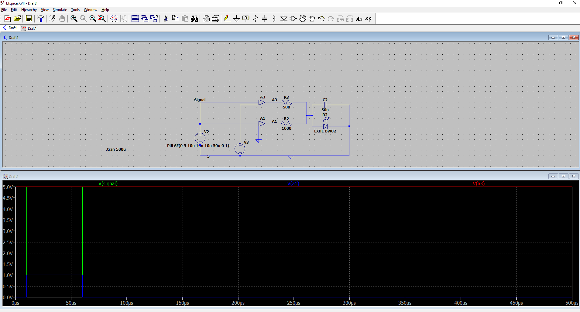
Hi

Ich versuche Aktuell eine Schaltung zu Simulieren. Aber aus einem mir
unbekannten Grund verhalten sich die Buffer nicht wie gedacht. Ich
dachte das der Mittlere Hintere Pin der Signal Eingang, der untere
Enable und der Rechte Ausgang ist. In dieser Schaltung sende ich ein
einzelnes Rechteck als Signal. In diesem Beispiel Sollte der obere
Buffer Enabled sein und der Untere nicht. Wie man aber am
Spannungsverlauf sieht ist das nicht wirklich der Fall.

Habe ich ein Falsches Modell für die Buffer (Standard Ltspice Buffer)
oder ist etwas an der Schaltung falsch was ich nicht erkenne.
Angehängte Dateien:
-

Unbenannt.png
41 KB
INV, BUF, AND, OR, and XOR are generic idealized behavioral gates. All
gates are netlisted with eight terminals. These gates require no
external power. Current is sourced or sunk from the complementary
outputs, terminals 6 and 7, and returned through device common, terminal
8. Terminals 1 through 5 are inputs. Unused inputs and outputs are to be
connected to terminal 8. The digital device compiler recognizes that as
a flag that that terminal is not used and removes it from the
simulation. This leads to the potentially confusing situation where AND
gates act differently when an input is grounded or at zero volts. If
ground is the gate's common, then the grounded input is not at a logic
false condition, but simply not part of the simulation. The reason that
these gates are implemented like that is that this allows one device to
act as 2-, 3-, 4- or 5- input gates with true, inverted, or
complementary output with no simulation speed penalty for unused
terminals. That is, the AND device acts as 12 different types of AND
gates.
Generell sind die Eingänge links. Der Pin ganz unten links ist der Pin
für das Bezugspotential. Wenn man an den nichts anschließt, dann ist das
Bezugspotential GND.
Im Gegensatz zu realen ICs sollte man in LTspice bei A-devices an
unbenutzte Pins bewusst nichts anschließen und zwar auch nicht GND. GND
wird eh immer ignoriert.

Im Anhang ist eine Datei die zeigt was man bei einem Gatter oder
D-flipflop so einstellen kann. In Flipflops muss immer mindestens einer
der Parameter td oder trise gesetzt sein damit die Flipflops zuverlässig
funktionieren.
Bitte melde dich an um einen Beitrag zu schreiben. Anmeldung ist kostenlos und dauert nur eine Minute.
Bestehender Account
Schon ein Account bei Google/GoogleMail? Keine Anmeldung erforderlich!
Mit Google-Account einloggen
Mit Google-Account einloggen
Noch kein Account? Hier anmelden.