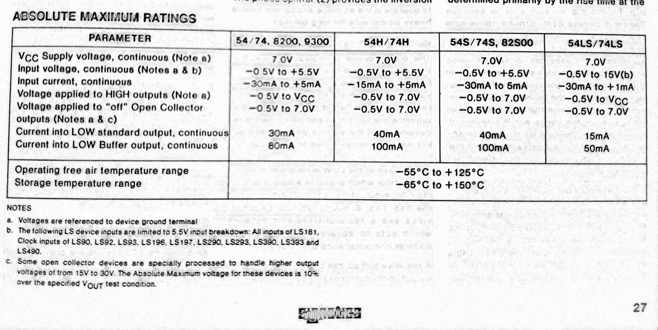
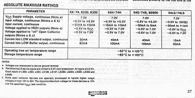
Input current, continuous
-30mA to +5mA
-15mA to +5mA
-30mA to 5mA
-30mA to +1mA
Voltage applied to HIGH outputs (Note a)
-0.5V to VCC
-0.5V to 7.0V
-0.5V to 7.0V
-0.5V to VCC
Voltage applied to "off" Open Collector outputs (Notes a & c)
-0.5V to 7.0V
-0.5V to 7.0V
-0.5V to 7.0V
-0.5V to 7.0V
Current into LOW standard output, continuous
30mA
40mA
40mA
15mA
Current into LOW Buffer, continuous
80mA
100mA
100mA
50mA
Operating free air temperature range
-55°C to +125°C
Storage temperature range
-65°C to +150
is activated every six oscillator periods except during external data memory access. PSEN remains high during internal program e x e c u t i o n . E A When held at a TIL high level, the 8051AH executes instructions from the i n t e r n a l Rw h e n t h PC is less t h a n 4096. W h e nheld at a TTL~-low
not, maybe reinstalling the app could fix things. Or perhaps changing the display settings to a higher contrast mode would help the new one with better visibility. Wait, what about the firmware? Maybe that's where the problem lies. I'll need to check if there are any known issues or patches for my specific
21621 Wrong / missing warning "skipping two-word instruction" 2.29.x 21849 Locate .progmemx.* at a higher address 2.29.x 21683 Support __gcc_isr pseudo-instruction 2.29 21583 Move .jumptables to a higher address 2.29 21569 Merge avr.sc and avrtiny.sc 2.29 21472 Add new emulation for ATtiny416 et al. (don't
Support ACCUMULATE_OUTGOING_ARGS 4.7.0 50775 Register allocator sets up frame and frame pointer with low register pressure 4.7.0, ra 50616 ICE: lto1.exe: invalid resolution in the resolution file 4.7.0, lto, mingw32 50566 Add support for better logging by means of -mlog= 4.7.0 50465 Use insn attribute
(z.B. Einzelne Zellpotenziale für die VC5 VC1=16.8V, VC2=12.6V, Überwachung VC3=8.4V...) DO (Pin HIGH (Spannung nahe VCC oder Entlade-MOSFET ist durchgeschaltet / 14) interner Reglerspannung, z.B. freigegeben >10V) CO (Pin HIGH (Spannung nahe VCC oder Lade-MOSFET ist durchgeschaltet / 15) interner Reglerspannung
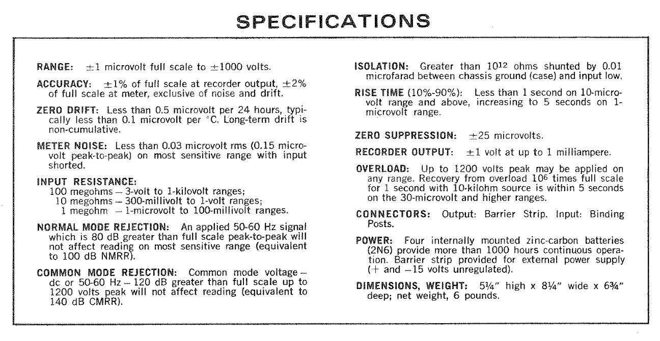
any range. Recovery from overload 10^6 times full scale within 5 seconds on the 30-microvolt and higher ranges.
CONNECTORS: Output: Barrier Strip. Input: Binding Posts.
POWER: Four internally mounted zinc-carbon batteries (2N6) provide more than 1000 hours continuous operation. Barrier strip provided for external power supply (+ and - 15 volts unregulated).
DIMENSIONS, WEIGHT: 5 1/4" high x 8 1/4" wide x 6 3/4" deep; net weight, 6 pounds.
: Target frequency 25 kHz, acceptable operational range 21 kHz to 28 kHz Maximum voltage for logic low: VIL = 0.8 V Absolute maximum current sourced: Imax = 5 mA (short circuit current) Absolute maximum voltage level: VMax = 5.25 V (open circuit voltage) This signal must be pulled up to a maximum of
2O04 93]f03[3]CP PINNING D HEF 401748 DotoDs datainputs 7 MR Og Do Dy 0; -D2 O02 Vss5 _ _ clockinput (LOW toHIGH edgetriggered) : [6] 8] MR masterresetinput(activeLOW) Pinningdiagram OotoOg bufferedoutputs F U N C T I O N T A B L E lcelo [im | o J |H H H J L H L : L I X H no change X |X PL L i, H = HIGH
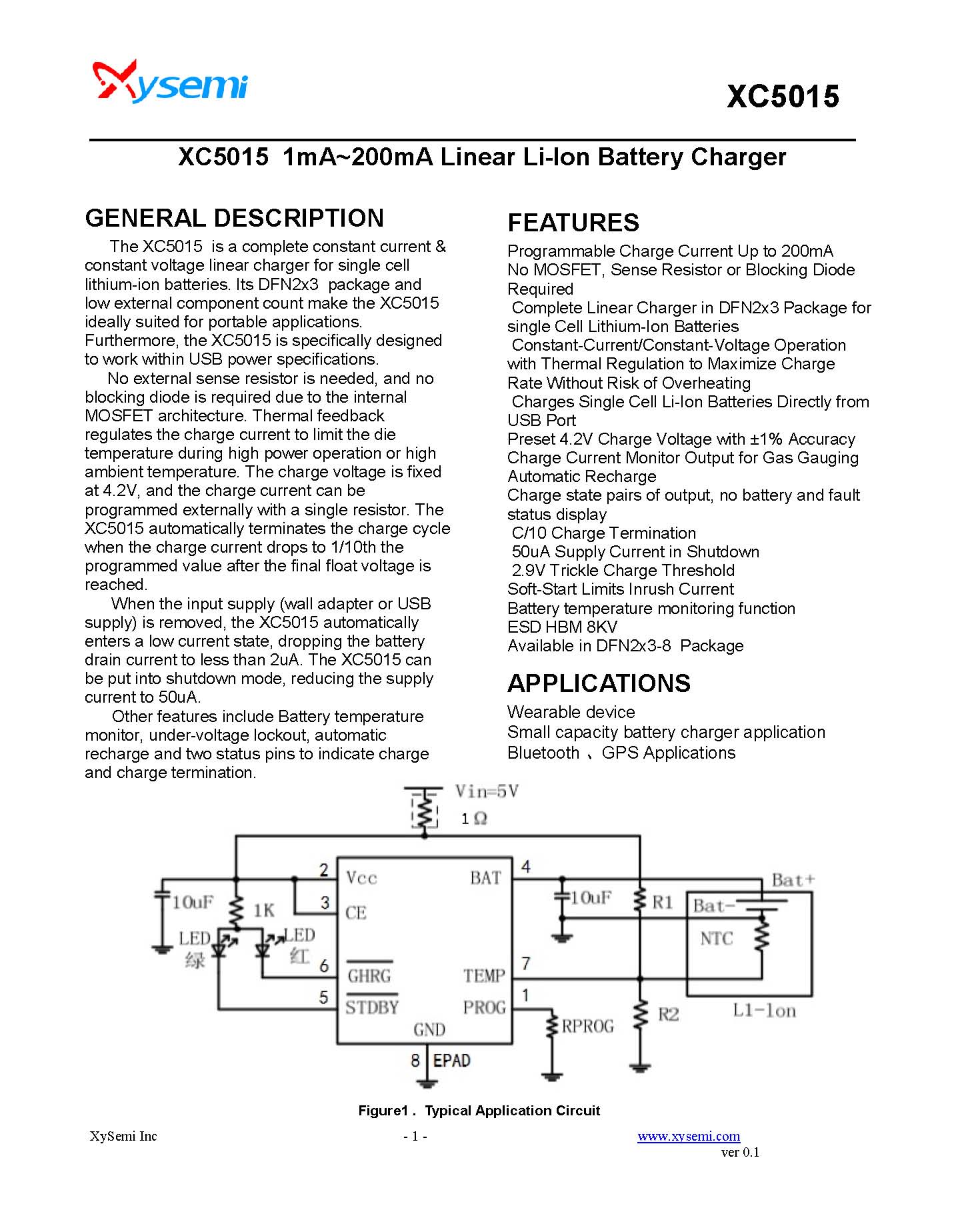
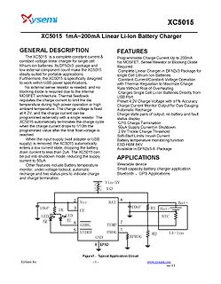
current & constant voltage linear charger for single cell lithium-ion batteries. Its DFN2x3 package and low external component make the XC5015 ideally suited for portable applications. Furthermore, the XC5015 is specifically designed to work within USB power specifications. No external sense resistor is needed
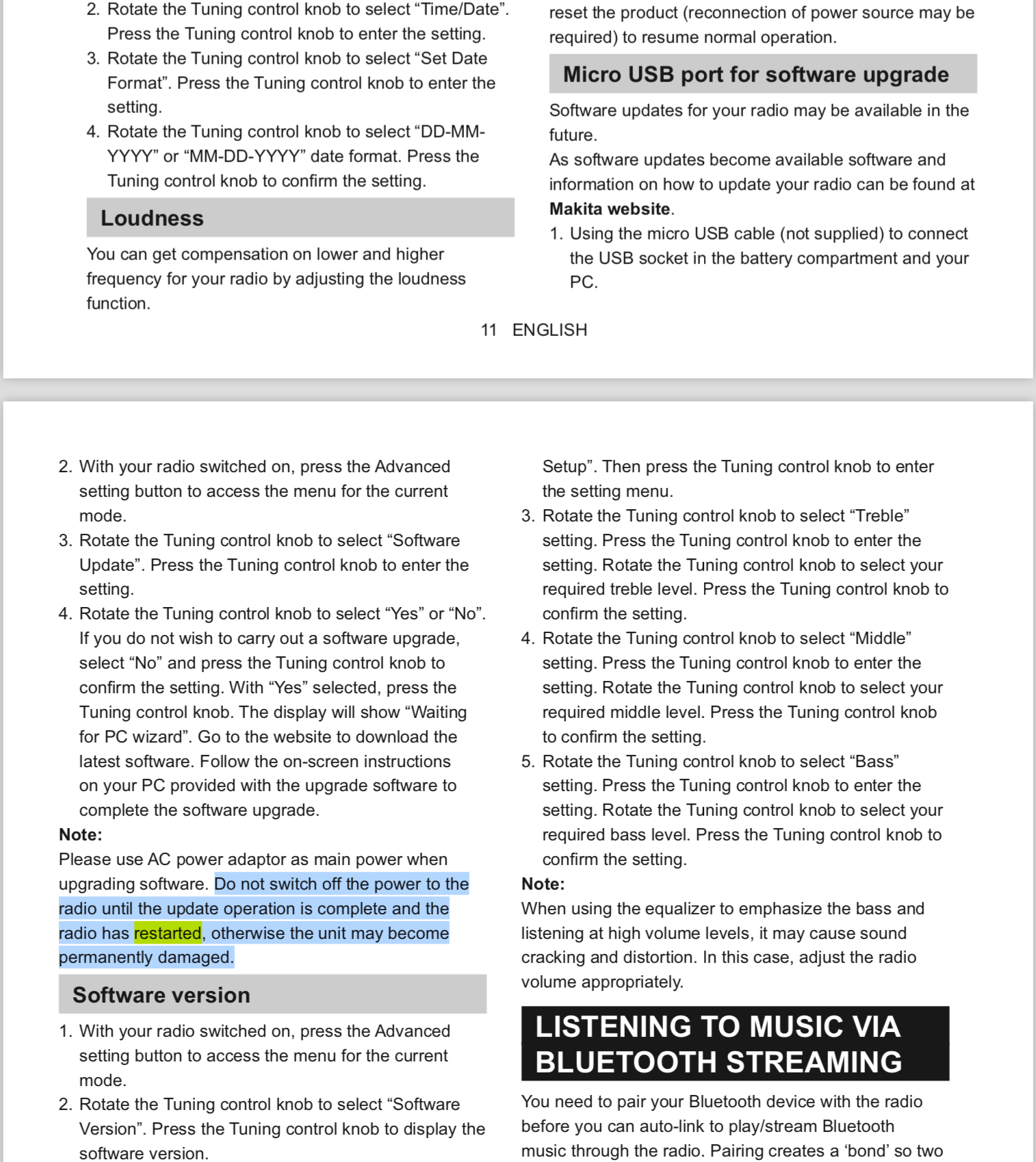
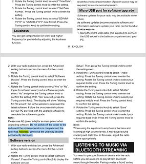
format. Press the Tuning control knob to confirm the setting. Loudness. You can get compensation on lower and higher frequency for your radio by adjusting the loudness function. Micro USB port for software upgrade. Software updates for your radio may be available in the future. As software updates become
reset voltage V DD= 6 V; no load; − 1.3 2.4 V V I V DDor VSS note 1 Input SCL; input/output SDA VIL LOW level input voltage −0.5 − +0.3VDD V V HIGH level input voltage 0.7V − V + 0.5 V IH DD DD OL LOW level output current V OL= 0.4 V 3 − − mA L leakage current V I V DDor VSS −1 − +1 A Ci input capacitance
Slave mode. Configure the method is as follows: PI0 (4)--soft/hardware master-slave set port: set low (or impending) for hardware Settings master-slave mode, set 3.3 V high level for software installed master-slave mode; If choose hardware Settings master-slave mode, can use the PIO (5) to set; If choose
stm32wba25ce.pdf Im Bereich des Funkmoduls hebt STMicroelectronics die folgenden Attribute hervor: [c] High‑performance radio delivering stable connectivity with +10 dBm max output power Supports Bluetooth® LE, Zigbee, and Thread for broad protocol compatibility Programmable Tx power in 1 dB steps
precisely tune energy consumption and extend battery life Flexible power‑control leveraging ultra-low-power STM32 MCU architecture for longer battery life [/c] Interessant ist, dass sich im Abschnitt zu den geringen Kosten nach folgendem Schema auch ein Hinweis auf die Optimierung des Layouts
150 RMI www.vishay.com Vishay BCcomponents Aluminum Electrolytic Capacitors Radial Miniature, Low Impedance FEATURES • Very long useful life: 4000 h to 10 000 h at 105 °C, high stability, high reliability • Very low impedance and low ESR in smaller case sizes than the 136 RVI series • Excellent
through the core. Sheathing There are three kinds of optical fiber: a) All-plastic fiber (APF) Cladding (low refractive index for confinement of light) b) Plastic-cladding silica Fiber (PCF) c) Silica fiber Core (high refractive index for transmission of light) APF is used for short-distance data transmission
resistors series have 8 sizes from 5W to 12W. Because with a ceramic substance, producing a resistor with high all our resistors are fully welded they can be used in electrical qualities and excellent mechanical strength. commercial as well as in industrial equipment. The terminals are made of nickel silver,
Datasheet Snubberless™, logic level and standard 16 A Triacs A2 Features • Medium current T riac G • Low thermal resistance with clip bonding A1 • Low thermal resistance insulation ceramic for insulated BTA A2 • High commutation (4Q) or very high commutation (3Q, Snubberless™) capability • BTA series UL1557
CA-C03 Specifications Features 1. Small size SMD patch antenna with size only 5.5 X 2.0 X 1.0 mm. 2. Low energy loss, high antenna efficiency. 3. High stability under temperature and humidity changes. Structure 1. Antennafeeder 2. Feeder identificationmark 3. Antenna welding fixed end Size Three View symbol
Icon links: offener Schalter MCU: ModA und ModB über Jumper auf Gnd ziehen Reset: 2. Icon von links: Low Pulse -> rote LED blitzt ->File -> Save Procect as... -> save in: [xc68hc711e20cfn] File name: [xc68hc711E20cfn_8MHz] Test: > L 0 -> liest 16 bytes ab RAM Adresse 0 > L 0 2ff -> liest das gesamte RAM
Ethos NPU, die bis zu 1,8 eTOPS erreicht. Das integrierte IW610-Tri-Radio vereint Wi-Fi® 6, Bluetooth® Low Energy sowie 802.15.4-Konnektivität und unterstützt Implementierungen von Matter und Thread. Dadurch entfallen aufwendige HF-Abstimmungen und Koexistenzprobleme, die Entwicklungs- und Zertifizierungsprozesse
undersampling-based RF measurements, and adds a new 5-slot Multi-Instrument Mode for running more high-speed instruments simultaneously. [/c] ### KiCad 10.0 verfügbar Die Weiterentwicklung der quelloffenen PCB-Software KiCad schreitet plangemäß voran. Unter der URL https://www.kicad.org/blog
) on-chip Calculation Unit as well as by the interrogating bit 31 bit 0 system. IDE Page 0 b31 SK (low) b0 Page 1 7.1.2 Password Basestation, PSW B X b47 SK (high) b32 Page 2 The Password Basestation, PSW , is apBlicable in TMCF b23 PSW T b0 Page 3 Password mode only (ENC = 0). The Password USER 0 Page
Extended IDs. 2004 von infineon abgekündigt, ohne Nachfolgeprodukt Bustreiber (CAN-Transceiver). High-Speed. MCP2551. von Microchip PDIP8 und SOIC VCC = 4,5...5,5V kostet rund 1 Datenblatt Eagle-Lib PCA 82C250. ABGEKÜNDIGT! In Produktion: NXP Orderlist von NXP (ex. Philips) PDIP8 und SO8 VCC = 4,5..
Base Chip (SBC) SO28 Serial Interface (SPI) Spannungsregler (LDO) CAN Repeater. AMIS-42700. Dual High-Speed CAN Transceiver High speed (up to 1Mbit/s) SOIC-20 vgl. Alternative. zwei Transceiver Schaltung Anmerkung: Diese Schaltung ist Quatsch und funktioniert nicht. -Zum Senden eines Zeichen, muss beim
there is only one active performance mode: 792 MHz. b) In standby/DSM mode the datasheet defines lower operating conditions for VDD_ARM_IN and VDD_SOC_IN, reducing power consumption and junction temperature. In this mode, the voltage and temperature are set low enough so that the effect on the lifetime
stehen die vier folgenden neuen Funktionen zur Verfügung: [c] • Modulino Latch Relay – Switch high-power loads with a simple signal • Modulino Light – Detect ambient brightness and react to changes in lighting • Modulino Joystick – Add intuitive interactive control to your gaming or robotics
nRF54L Series. . . . Uniquely, the nRF54LV10A is also the world’s first Bluetooth LE SoC to combine low voltage with Bluetooth Channel Sounding support. – via https://www.nordicsemi.com/Nordic-news/2025/12/Nordic-unveils-nRF54LV10A-a-breakthrough-low-voltage-Bluetooth-LE-SoC [/c] Ebenda findet sich
leads to Eisen Banddi- stat. striktion stand cke • kleinere Ummagnetisierungsverluste bei hohen In- • lower magnetic losses at high inductions Average Satu- Stat. Satu- spec. duktionen • higher permeability Main values ration for tape Permeability ration coerci- magne- Curie- electri- Density • höhere Permeabilität
, , 1 a 0 m ø , 2 1,0 All dimensions in mm typical APPLICATIONS DESCRIPTION IoT The MS1V-T1K is a low frequency surface mount technology Quartz Metering Crystal Unit that incorporates a tuning fork Quartz Crystal Resonator. It Wearables operates under vacuum in a hermetically sealed square-bodied metal Health Care can package. Consumer Electronics FEATURES High stability is guaranteed by hermetic sealing. High shock and vibration resistant. Proven surface mount technology package for reflow soldering. Excellent lead coplanarity for surface mounting. RoHS-compliant
XNOR: u out= 0.5· 1 + ui,m (11.270) m The above-mentioned functions model devices with 0V as logical low-level and 1V as logical high- level. Of course, they can be easily transformed into higher voltage levels by multiplying the desired high-level voltage to the output voltage uoutand dividing the input
Einführung Introduction Herzlichen Glückwunsch zum Erwerb dieser Congratulations on purchasing this high-tech High-Tech Entlötstation von ERSA. ERSA desoldering station. SieverwendendieseGerätekombinationvorzugs- We recommend that you use this combination weise zum Entlöten bedrahteter Bauelemente unit
Glass-Passivated Junctions for Parameter Uniformity and Stability • Small, Rugged Thermowatt Construction for Low Thermal G A K Resistance, High Heat Dissipation and Durability • Low Trigger Currents, 200 mA Maximum for Direct Driving from Integrated Circuits • Pb−Free Packages are Available* MAXIMUM RATINGS (TJ
industry, the EDM sealed tact keyswitches are used in a variety of instrument panels, giving users a high-performance, long-lasting switch with great tactile feedback. EDM keyswitches are built for short travel and are self-cleaning, with three actuation forces available. Features & Benefits ■ Short travel
mode. The temperature in the sauna room is lower (approx. 40 to 65 °C) than in sauna mode, with the relative humidity being considerably higher, spanning 35% to approximately 70%. The maximum humidity level which can be set depends on the temperature of the sauna. The higher the sauna temperature, the lower the maximum humidity level which can be set. The indicator light4 , 5 and b -g are green during climate mode. WORLD OF WELLNESS Heruntergeladen von manualslib.de Handbücher-Suchmachiene
1029 U, S III, S IV 111-1, IV-1 7-5, 10-12 Uan6 H {>n III-2, IV-2 6-5, 11-12 L IUp) Steuerspannung HIGH: $ USH = 3,3 V Eingangssperrstrom HIGH: sh = 1 PA 11 Steuerspannung LOW: USL =2,1 V i Steuerstrom LOW: - /SL = 200 pA i Schalter- Steuerung Schaltersteuerung TDA 1029 11 11 11 Eingeschaltete Durchgeschaltete
Supply (+5V) I Register Select: "1" = Command Register, “0” = Data Register I Read Select (Active Low) - MPU ⇐ T6963C I Write Select (Active Low) - MPU ⇒ T6963C I Chip Enable (Active Low) DB0 I/O Bi-directional Data Bus Line 0 DB1 I/O Bi-directional Data Bus Line 1 DB2 I/O Bi-directional Data Bus Line
ports will change according to various patterns, depending on the reference weight limit and on the lower and upper weight limits. Example: Control lines used only within check range: Lower limit 30%; upper limit ∞% from setpoint Menu code: 4 3 2* 30% Setp. Min. Setpoint Max. “L” “H” LOW < OK = HIGH > SET Note: When not in use, the voltage level is high: >2.4 V/+2 mA. When in active use, the voltage level is low: <0.4V/–2 mA. Caution: the output ports are not protected against short circuits! 4–17 Pin Assignment Chart for12-pin Round Connector Interface
bi-directional transparent data transmission. It is easy to use, along with features like fast data rate, low power consumption, high stability, suits applications such as safety & security, IoT, and so on. More (http://www.waveshare.com/2-CH-UART-TO-ETH.htm) (http://www.waveshare.com/2- CH-UART-TO-ETH.htm?
2 N 3 8 2 0 2N3820 P-Channel General Purpose Amplifier This device is designed primarily for low level audio and general purpose applications with high impedance signal sources. Sourced from process 89. 1 TO-92 1. Drain 2. Gate 3. Source Epitaxial Silicon Transistor Absolute Maximum Ratings* TC

 Bild
 Bild

 Bild
 Bild
 Bild
 Bild
 Bild
 Bild
 Bild
 Bild
 Bild