Application Note 50
Vishay Semiconductors
Using the IL300 Optocoupler
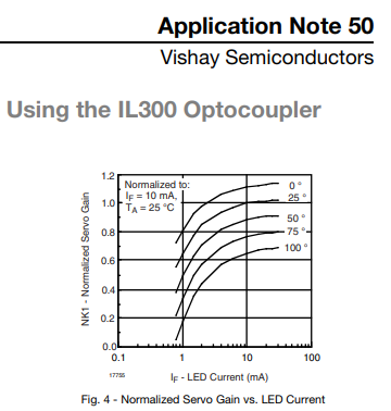
1.2
1.0
0.8
0.6
0.4
0.2
0.0
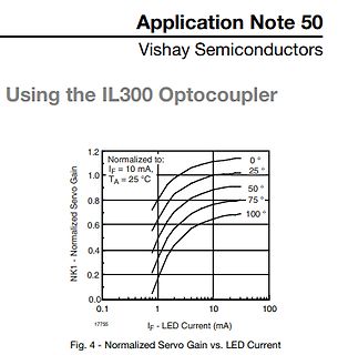
NK1 - Normalized Servo Gain
0°
25°
50°
75°
100°
Normalized to:
IF = 10 mA,
TA = 25 °C
0.1
1
10
100
IF - LED Current (mA)
Fig. 4 - Normalized Servo Gain vs.
footprint and electrical schematic process control system.Their low level DC and AC signal must of the IL300.The following sections discuss the key operating be accurately measured in the presence of high common characteristics of the IL300.The IL300 performance character- mode noise.The IL300’s 130 dB common
Ratings Rated voltage after 5 minuets Equivalent Series Refer to Standard Ratings Measurement freq. : 300kHz-500kHz Resistance (ESR) Permissible Ripple Current Refer to Standard Ratings Measurementfreq. : 300kHz-500kHz, sinewave Δ C/C tan δ LC Surge voltage test +20%〜−20%oftheinitialvalue Within IL Within
Man braucht keinen > Super-Duper Optokoppler plus Beschaltung. Quatsch. Dein Video nutzt den IL300. Es vergleicht Feedback mit solchen linearen Optokopplern mit dem digitalen Feedback eines TL431. Die Schleifenkompensation muss dann eben auf die Sekundärseite. Ein TL431 ist ein Komparator
Beitrag #8036436: > Quatsch. In der Tat. Das ist deine Kernkompetenz. > Dein Video nutzt den IL300. Du solltest es bis zum Ende anschauen. > Es vergleicht Feedback mit solchen linearen Optokopplern mit dem > digitalen Feedback eines TL431. Schon wieder falsch. Der TL431 hat eine lineare
http://cq-cq.eu/DJ5IL_rt006.pdf mit der Bildersuche entdeckt. DJ5IL_rt006.pdf Originalversion: 22.12.2014 https://vm.schwaben-tech-park.de/telefunken-virtuelles-museum/buschbeck-messinstrument https://50ohm.de/photos
nicht zu den Fotos, denn da sind auf 10 cm immerhin 4 LEDs, das wären dann mit einem Dreisatz auf 300 cm schonmal 120 LEDs.
nicht zu den Fotos, denn da sind auf 10 cm > immerhin 4 LEDs, das wären dann mit einem Dreisatz auf 300 cm schonmal > 120 LEDs. Schau mal im Beitrag #7990870. Ich habe mich korrigiert. 130 Stück sind es.
ACPL-C870 Vollintegrierter, optischer, analoger Trennverstärker, arbeitet intern jedoch digital Vishay IL300 Solid State Optronics SLC800 mit Applikationshinweis Isolink OLH7000 IXYS (Clare) LOC211P (Anti)Dual Linear Optocoupler IXYS (Clare) LOC210P (Anti)Dual Linear Optocoupler IXYS (Clare) LOC117 Single
Verpolungs- und Überspannungsschutz mit Photo-MOS Forumsbeitrag: Lineare Spannungsübertragung mit IL300 Forumsbeitrag: Hinweise zum ACPL-C870 Forumsbeitrag: Lebensdauer Optokoppler Forumsbeitrag: warum hier zwei Vorwiderstände (Gleichtaktstörungen bei schnellen Gatetreibern mit Digitalkoppler) Forumsbeitrag
Serienwiderstand (Größenordnung 150 Ohm) und die Haupt-Magnetisierungs-Induktivität (Größenordnung 300 mH) ein LR-Hochpass bildet. Man muss die Übertrager also unbedingt niederohmig ansteuern. Noch besser: Serienwiderstand kompensieren durch eine NIC-Schaltung. Beispielschaltungen weiter unten auf
Internet findet man vieles, was einfach aussieht und einfach nichts taugt. Die nutzen nicht mal einen IL300.
Komparatoren Schaltplan A A a 08 08b Qi3a . Giâbl Ghe 4 a 29|] | o3 pr pa & . gr 25 Uhr 9 Az 022 | az pe IL) 05 06 0» lu [E Nein u R3 [in2 er PR Geben TERMINALKONFIGURATION (Draufsicht) NC. Li LI] [a] NC Ne. —2 ne ML mc. ne RO Il IN n pe nu O O ve NUL Li NC Ne —s m izquiere IN —2 7 n-Q Oesire v- —s snm INe—p
Dafür gibt es diverse Standardlösungen. a) Isolationsverstärker, entwerder selbst gestrickt (Z.B. IL300 Optokoppler) oder vollintegriert (ACPL-C870). https://www.mikrocontroller.net/topic/431716#5087308 b) Current sense amplifier, kann man auch selber bauen (OPV + PNP Transistor) oder fertig kaufen
± 20 % R Rated RMS ripple current at 100 kHz, 105 °C Nominal case size: Ø 10 mm x 12 mm; Form TFA IL2 Max. leakage current after 2 minRat U tan δ Max. dissipation factor at 100 Hz Ordering code: MAL215035471E3 Former 12NC: 2222 150 35471 Z Max. impedance at 100 kHz Note • Unless otherwise specified,
Therefore, the peak current IL(P)seen by the inductor is calculated with Equation 5. ’IL(P P) L(P) IL(DC)▯ 2 (5) Inductor values can have ±20% tolerance with no current bias. When the inductor current approaches saturation level,
6. Il y a des pièces défectueuses dans l’ensemble de (déformations, fissures, signes de gondolement, etc.) production et de transmission de micro-ondes. de la plaquette avant de la cavité. 7. Il y a des détériorations
6. Il y a des pièces défectueuses dans l’ensemble de (déformations, fissures, signes de gondolement, etc.) production et de transmission de micro-ondes. de la plaquette avant de la cavité. 7. Il y a des détériorations
Analog Output Voltage range VAVx IV 0 2.9 V Digital Inputs Logic compatibility CMOS Logic “0” voltage V IL I 0 0.8 V Logic “1” voltage V IH I 2.3 VCC V Logic “0” current IL I -10 0 µA Logic “1”current IH I 0 10 µA TPE logic “0” voltage IILPE 1 -10 0 µA TPE logic “1” voltage IHTPE 1 0 100 µA Digital Outputs
200 ms reset. Serial Interface CMOS (Asynchronous) 3.3V-level signals. Rate is software selectable (300 bps to 921600 bps) Serial Line Formats 7 or 8 data bits, 1-2 Stop bits, Parity: odd, even, none Modem Control DTR/DCD, CTS, RTS Flow Control XON/XOFF (software), CTS/RTS (hardware), none Programmable
200 ms reset. Serial Interface CMOS (Asynchronous) 3.3V-level signals. Rate is software selectable (300 bps to 921600 bps) Serial Line Formats 7 or 8 data bits, 1-2 Stop bits, Parity: odd, even, none Modem Control DTR/DCD, CTS, RTS Flow Control XON/XOFF (software), CTS/RTS (hardware), none Programmable
der Sonne ist, dessen Radio laut läuft und sich selber weiter aufheizt und das vielleicht gerade 300km über die Autobahn gefahren ist und die Hitze aus dem Motorraum langsam durch die Spritzwand dringt - Da könnte ich mir schon 100°C im Autoradio als Worst Case vorstellen und da plane ich zur Sicherheit
15 15.5 mA Input current II VI=VDDV SS —— —— ±1 µA V IH DIN,ET 0.7VDD —— —— V Input voltage level V IL DIN,ET —— —— 0.3 DD V Hysteresis voltage V D SET —— 0.35 —— V H IN, Switching Characteristics(T =-20~+70℃, V =4.5~5.5V, V =0V, unless otherwise specified) A DD SS Parameter Symbol Condition Min Tpy Max
- Mode V CC E G W DQ7 Power Deselect V X X High Z Standby IH WRITE 4.75 to 5.5 V V X V D Active or IL IL IN READ VIL V IL V IH D OUT Active 4.5 to 5.5 V READ VIL VIH V IH High Z Active (1) Deselect V SO to PFD (min) X X X High Z CMOS standby (1) Deselect ≤ VSO X X X High Z Battery backup mode 1. See
s, NRZ) (nm) (m) (1) (ns)(1) (V) (°C) (µm) with Fiber-Optic Connectors TODX296 Up to 1000 PCF (200/300) TOCP200Q - BTOCP200X - B DC to 6 800 ± 55 5 ± 0.25 – 40 to 85 Up to 800 H PCF(200/230) CF-2071 Series (5) TODX298 (2) Up to 1000 PCF (200/300) TOCP200Q - BTOCP200X - B DC to 8 800 ± 42 5 ±0.25 – 40
A recessive (VINH= VBAT; V LIN= VBAT; V = V ; NWAKE BAT V TXD= 0 V; VNSLP= 0 V) standby mode; bus 300 900 2000 A dominant (VBAT = 12 V; V INH= 12 V; LIN= 0 V; V = 12 V; NWAKE V TXD= 0 V; V NSLP= 0 V); note 3 low slope mode; bus 100 400 1000 A recessive (VINH= VBAT; V LIN= VBAT; V NWAKE = VBAT; V TXD
Programmtexten liegt der Schwerpunkt völlig anders. Da ist – im besten Fall – eine klare Unterscheidung IlL1, 0O, usw. wichtig. Man kann schön sehen, wie 'zerrissen' der Serifenlose Text erscheint.
Frank war vollkommen ok. Man sieht ja wie sich der Thread weiterentwickelt. Aus dem Thread könnten 300 Kommentare gelöscht werden, ohne dass der Thread irgendeinen Schaden nimmt. Soviel Unselbstständigkeit einiger User wie in diesem Thread ist mir lange nicht begegnet.
Logic “0” voltage VIL I 0 0.8 V Logic “1” voltage V I 2.3 VCC V IH Logic “0” current I I -10 0 µA IL Logic “1”current I I 0 10 µA IH TPE logic “0” voltage I TPE 1 -10 0 µA IL TPE logic “1” voltage IIHPE 1 0 100 µA Digital Outputs Logic compatibility CMOS Logic “0” voltage1) VOL I 0.6 V Logic “1” voltage1
°C +125 °C Min Typ Max Min Max Min Max 74HC4851 R ON resistance V = V to GND; E = V ON(peak) I CC IL (peak) VCC = 2.0 VSWI= 2 mA - 400 650 - 670 - 700 Ω VCC = 3.0 VSWI≤ 2 mA - 215 330 - 360 - 380 Ω VCC = 3.3 VSWI≤ 2 mA - 120 270 - 305 - 345 Ω V = 4.5 V; I≤ 2 mA - 76 210 - 240 - 270 Ω CC SW VCC = 6.0 VSWI≤ 2 mA - 59 195 - 220 - 250 Ω ΔR ON ON resistance VI= 0.5 × CC; E = IL mismatch between VCC = 2.0 VSWI= 2 mA - 4 10 - 15 - 20 Ω V = 3.0 V; I≤ 2 mA - 2 8 - 12 - 16 Ω channels CC SW VCC = 3.3 VSWI≤ 2 mA - 2 8 - 12 - 16 Ω VCC = 4.5 VSWI≤ 2 mA - 2 8 - 12 - 16 Ω VCC = 6.0 VSWI
HEXADECIMAL DISPLAY WITH INTEGRAL TTL CIRCUIT TO ACCEPT, STORE, AND DISPLAY 4-BIT BINARY DATA D 0.300-Inch (7,62-mm) Character Height D Internal TTL MSI Chip With Latch, Decoder, D High Brightness and Driver D Operates from 5-V Supply D Left-and-Right-Hand Decimals D Constant-Current Drive for Hexadecimal
C [µFR*U [V]+6RA[µA] , c Usefullife3000h @85°C;U ;I R R Requirements o ΔC/C≤30% ofinitialvalue;ESR≤300%ofspecified; n u limitIL≤specifiedlimit t w Endurancetest2000h@85°C,U R Requirements t ΔC/C≤20%ofinitialvalue;ESR≤130%ofspecified; e limitI ≤specifiedlimit o L r , ClimaticcategoryIEC60068 40/085/56
C [µFR*U [V]+6RA[µA] , c Usefullife3000h @85°C;U ;I R R Requirements o ΔC/C≤30% ofinitialvalue;ESR≤300%ofspecified; n u limitIL≤specifiedlimit t w Endurancetest2000h@85°C,U R Requirements t ΔC/C≤20%ofinitialvalue;ESR≤130%ofspecified; e limitI ≤specifiedlimit o L r , ClimaticcategoryIEC60068 40/085/56
Adjust the under a max. temperature of 30 °C, 60 % RH after temperature of the soldering iron below 300 °C opening the dry pack envelope • Finish soldering within 3 s • Set the furnace temperatures for pre-heating and heating • Handle products only after the temperature has cooled off in accordance with
Differential Input, 600 kΩ Receiver Input Capacitance CRFI f=77.5 kHz 1.1 pF Input Levels IN |<0.5 µA V IL 0.35 V V IH VDD0.35 Output Current |OUT 5 15 µA V <0.2 V ;V >0.8 V OL DD OH DD DCF77 Output Pulses T 100ms 1 µVrms ≤ V IN 95 ms T 200ms 20 mVrms, see note below! 195 MSF Output Pulses T 1 µVrms ≤ V ≤
llu n g d e r M eßprotokolle und zu r Durchführung d e r E i n s t e l l a rb e ite n am R e g e lte il ( im ausgebautem Z u s ta n d ) , e r f o lg t d ie Strom versorgung am S t i f t 8 m it + 30V von einem e x te rn e n S trom versorg g u n g sg erät. Dokum entieren S ie Ih re A rb e it. Sehen S ie
lfürge fährUchee der interenUmsc hlagseite. Spannnungen. Weite re Infor ationen zur Sicherheitshinweise IL I Sicherhheit ud zum Ge - räuschpegell bef nden sich uf Allgemein s de hi nteren U mschllagseite. Symbol ür Erde. Vo r er Inbetriebnahme h at derB enuttzer diesss Prodxdct sowie die dazugehörigen un
V OUT VIN C IN 976 K COUT +E 4.7µF V 10µF I EN FB A K 562 K A - GND L1 4.7µH VOUT V IN SW 5.0V @ 300 mA 3.0V to 4.2V V OUTS VIN V OUTP 976 K + CIN C OUT N 4.7µF EN VFB 10 µF O I 309 K L - P GND SGND Efficiency vs. I OUT for 3.3V OUT 100.0 VIN 2.5V ) % 80.0 y c e c VIN 0.8V VIN 1.2V f E 60.0 40.0
Power CC Deselect V X X X High Z Standby IH Deselect 4.75 to 5.5 V X VIL X X High Z Standby WRITE or V IL VIH X VIL DIN Active READ 4.5 to 5.5 V V V V V D Active IL IH IL IH OUT READ V IL VIH V IH VIH High Z Active Deselect V SO to PFD X X X X High Z CMOS standby (min)1) (1) Deselect ≤ VSO X X X X High Z
VI= V SS - 4.4 5 pF I/Os V IL LOW-level input voltage 0.5 - +0.8 V V IH HIGH-level input voltage 2.0 - 5.5 V I LOW-level output current V = 0.4 V OL OL VDD = 2.3 V [3]9 - - mA VDD = 3.0 V [3]12 - - mA [3] VDD = 5.0 V 15 - - mA VOL
separaIely) V –2.5 7.5 V High-level input voltaIH, V D, R 2 V Low-level input voltage, V D, R 0.8 V IL Differential input volIDg(see Figure 5) –6 6 V Input voltage(Rs) 0 VCC V Input voltage for standby or s(Rs), V 0.75 VCC VCC V Wave-shaping resistance, Rs 0 100 kΩ Driver –40 High-level output currOHt
voltages than 5 Volt, e.g. 12 Volt. The I/O levels for fixed level devices are: LOW level input voltage V IL min. -0.5V max. 1.5V HIGH level input voltage V IH min. 3.0V max. V DDmax+0.5V LOW level output voltage V OL1 min. 0V max. 0.4V HIGH level output voltage V OH open drain output, determined by V DDvia
voltages than 5 Volt, e.g. 12 Volt. The I/O levels for fixed level devices are: LOW level input voltage V IL min. -0.5V max. 1.5V HIGH level input voltage V IH min. 3.0V max. V DDmax+0.5V LOW level output voltage V OL1 min. 0V max. 0.4V HIGH level output voltage V OH open drain output, determined by V DDvia
package. For applications with input voltage 6V or below, see MIC37xxx LDOs. Package Types MIC29150/300/500 MIC29151/301/501/751 3-Lead TO-220 (T) 5-Lead TO-220 Fixed Voltage (T) (Top View) (Top View) 5 FLG 3 OUT 4 OUT A 2 GND B T T 3 GND 1 IN 2 IN 1 EN 2016-2019 Microchip Technology Inc. DS20005685B-page

 Bild
Bild