-
Bild
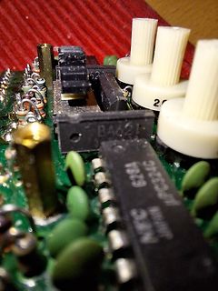
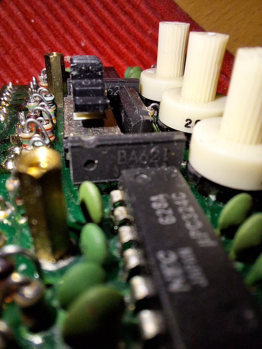
Nahaufnahme einer Leiterplatte mit integrierten Schaltkreisen
BA621 628A MPC324C JAPAN
in „Pinlayout des BA621 von Rohm“ · Analoge Elektronik und Schaltungstechnik · · Platinenfotos
-
Datei
c64.asm
; C64 includes ; SID SID_FREQLO1 = $D400 SID_FREQHI1 = $D401 SID_PWLO1 = $D402 SID_PWLHI1 = $D403 SID_CR1 = $D404 SID_AD1 = $D405 SID_SR1 = $D406 SID_FREQLO2 = $D407 SID_FREQHI2 = $D408 SID_PWLO2 = $D409 SID_PWLHI2 = $D40A SID_CR2 = $D40B SID_AD2 = $D40C SID_SR2 = $D40D SID_FREQLO3 = $D40E SID_FREQHI3 = $D40F SID_PWLO3 = $D410 SID_PWLHI3 = $D411 SID_CR3 = $D412 SID_AD3 = $D413 SID_SR3 = $D414 SID_FCLO = $D415 SID_FCHI = $
in „Wettkampf Opa(MOS6502) gegen Frischling(ATmega)“ · Mikrocontroller und Digitale Elektronik ·
-
PDF
FD6287T_fortiorEnglish.pdf
ratings (unless otherwise specified, all pins are referenced to COM). parameter symbol scope unit High-side floating absolute voltage -0.3ÿ275 In VB1,2,3 High-side floating offset voltage, VS1,2,3 VB1,2,3-25ÿVB1,2,3+0.3 In high-side output voltage, VHO1,2,3 VS1,2,3-0.3ÿVB1,2,3+0.3 In low-side supply voltage
in „hc-160a s2 Datenblatt?“ · Mikrocontroller und Digitale Elektronik ·
-
PDF
C906560.pdf
Thermistor 17 NU Low−side Emitter Connection − Phase U 18 NV Low−side Emitter Connection − Phase V 19 NW Low−side Emitter Connection − Phase W 20 W Phase W Output / High−side Floating Supply Offset Voltage 22 VBW High−side Floating Supply Voltage − Phase W 26 V Phase V Output / High−side Floating Supply Offset Voltage 28 VBV High−side Floating Supply Voltage − Phase V 32 U Phase U Output / High−side Floating Supply Offset Voltage 34 VBU High−side Floating Supply Voltage − Phase U 38
in „Ersatz für ON-Semi STK5Q4U362J-E / STK5Q4U363J-E bzw. passt da NFAQ1060L33T / NFAQ1060L36T“ · Analoge Elektronik und Schaltungstechnik ·
-
Bild
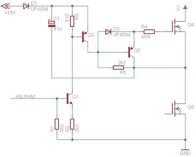
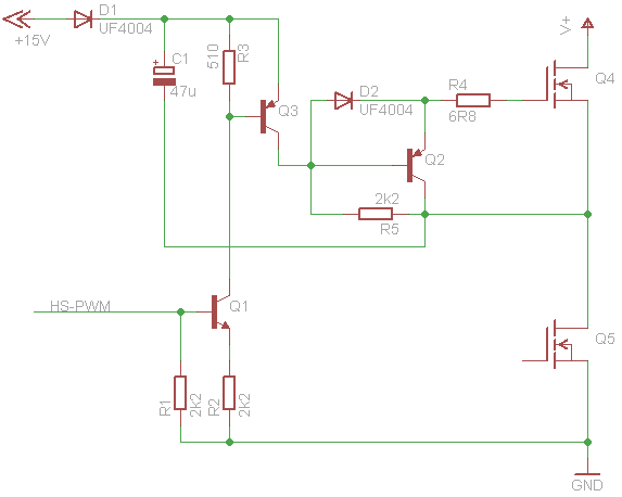
Schaltplan einer Transistorbeschaltung
+15V D1 UF4004 C1 47u R3 510 Q3 D2 UF4004 R4 Q4 V+ Q2 2k2 R5 HS-PWM Q1 R1 2k2 R2 2k2 Q5 GND
in „Gate Treiber diskret“ · Analoge Elektronik und Schaltungstechnik · · Schaltpläne
-
Bild
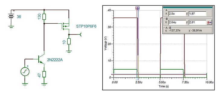
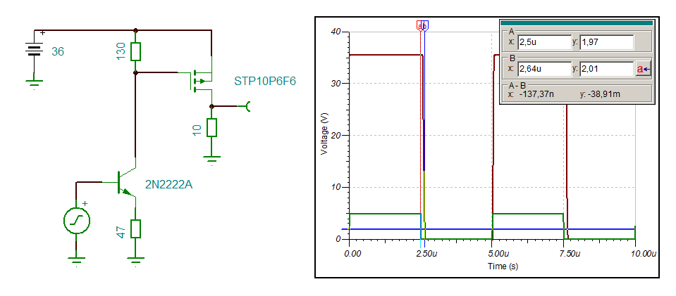
Schaltplan und Oszilloskop-Messkurve
36 130 STP10P6F6 10 2N2222A 47 40 30 20 10 Voltage (V) 0.00 2.50u 5.00u 7.50u 10.00u Time (s) A x: 2,5u y: 1,97 B x: 2,64u y: 2,01 A - B x: -137,37n y: -38,91m
in „Gate Treiber diskret“ · Analoge Elektronik und Schaltungstechnik · · Screenshots
-
Bild
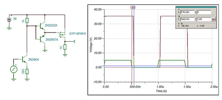
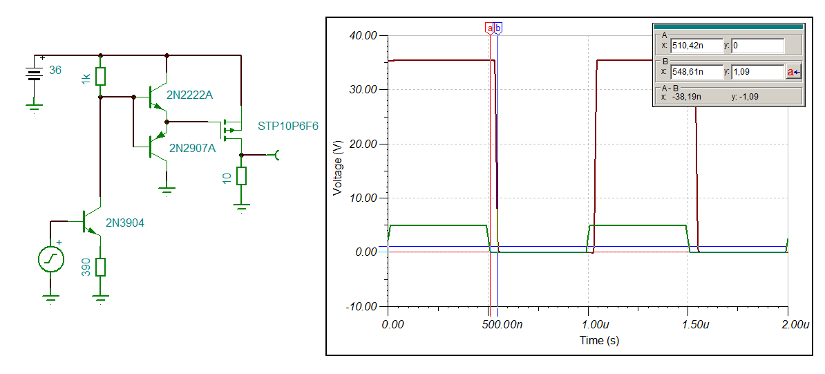
Schaltplan und Oszilloskop-Messkurve
36 1k 2N2222A STP10P6F6 2N2907A 10 2N3904 390 40.00 30.00 20.00 10.00 0.00 -10.00 Voltage (V) 0.00 500.00n 1.00u 1.50u 2.00u Time (s) A x: 510,42n y: 0 B x: 548,61n y: 1,09 A - B x: -38,19n y: -1,09
in „Gate Treiber diskret“ · Analoge Elektronik und Schaltungstechnik · · Screenshots
-
Bild
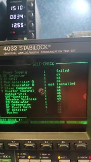
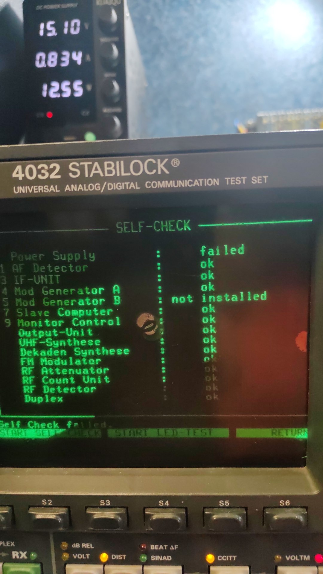
Display eines Stabilock Kommunikations-Testsets mit Fehlermeldung
15.10 0.834 12.55 4032 STABILOCK UNIVERSAL ANALOG/DIGITAL COMMUNICATION TEST SET SELF-CHECK Power Supply failed 1 AF Detector ok 3 IF-UNIT ok 4 Mod Generator A ok 5 Mod Generator B not installed 9 Slave Computer ok Monitor Control ok Output-Unit ok UHF-Synthese ok Dekaden Synthese ok FM Modulator ok RF Attenuator ok RF Count Unit ok RF Detector ok Duplex ok Self Check failed. START SELF CHECK START LED-TEST RETURN S2 S3 S4 S5 S6 DUPLEX RX VOLT DIST SINAD CCITT VOLTM
in „Willtek Schlumberger Stabilock 4031 4032“ · HF, Funk und Felder · · Fotos
-
PDF
NFAQ1060L33T-D.PDF
Diagram www.onsemi.com 3 NFAQ1060L33T Table 1. PIN FUNCTION DESCRIPTION Pin Name Description 1 VSS Low−Side Common Supply Ground 2 VDD Low−Side Bias Voltage for IC and IGBTs Driving 3 HIN(U) Signal Input for High−Side U Phase 4 HIN(V) Signal Input for High−Side V Phase 5 HIN(W) Signal Input for High−Side
in „Ersatz für ON-Semi STK5Q4U362J-E / STK5Q4U363J-E bzw. passt da NFAQ1060L33T / NFAQ1060L36T“ · Analoge Elektronik und Schaltungstechnik ·
-
PDF
NFAQ1560R43T-D.PDF
Block Diagram www.onsemi.com 3 NFAQ1560R43T PIN FUNCTION DESCRIPTION Pin Name Description 1 VSS Low−Side Common Supply Ground 2 VDD Low−Side Bias Voltage for IC and IGBTs Driving 3 HIN(U) Signal Input for High−Side U Phase 4 HIN(V) Signal Input for High−Side V Phase 5 HIN(W) Signal Input for High−Side
in „Ersatz für ON-Semi STK5Q4U362J-E / STK5Q4U363J-E bzw. passt da NFAQ1060L33T / NFAQ1060L36T“ · Analoge Elektronik und Schaltungstechnik ·
-
PDF
STK5Q4U362J-E-D.PDF
DESCRIPTION Pin Name Description 1 GND Negative Main Supply 2 VDD +15 V Main Supply 3 HINU Logic Input High Side Gate Driver - Phase U 4 HINV Logic Input High Side Gate Driver - Phase V 5 HINW Logic Input High Side Gate Driver - Phase W 6 LINU Logic Input Low Side Gate Driver - Phase U 7 LINV Logic Input Low Side
in „Ersatz für ON-Semi STK5Q4U362J-E / STK5Q4U363J-E bzw. passt da NFAQ1060L33T / NFAQ1060L36T“ · Analoge Elektronik und Schaltungstechnik ·
-
Bild
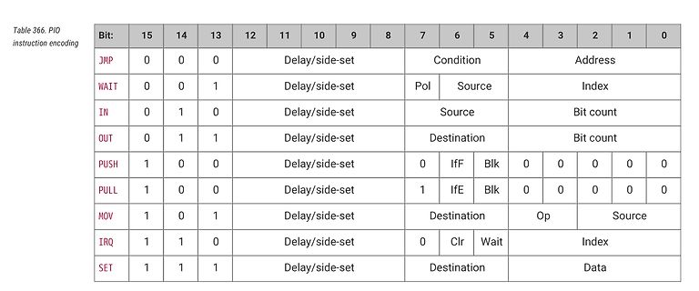
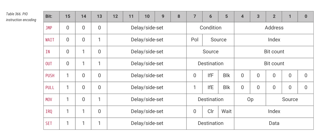
Tabelle der PIO Befehlskodierung
Table 366. PIO instruction encoding Bit: 15 14 13 12 11 10 9 8 7 6 5 4 3 2 1 0 JMP 0 0 0 Delay/side-set Condition Address WAIT 0 0 1 Delay/side-set Pol Source Index IN 0 1 0 Delay/side-set Destination Bit count OUT 0 1 1 Delay/side-set Destination Bit count PUSH 1 0 0 Delay/side-set 0 IfF Blk 0 0 0 PULL 1 0 0 Delay/side-set 1 IfE Blk 0 0 0 MOV 1 0 1 Delay/side-set Destination Op Source IRQ 1 1 0 Delay/side-set 0 Clr Wait Index SET 1 1 1 Delay/side-set Destination Data
in „PiPico PIO programmieren“ · Mikrocontroller und Digitale Elektronik · · Screenshots
-
PDF
slva963.pdf
running at 8-A continuous output, and left for a period of time to come to thermal equilibrium. The top-side plot was recorded from above while the bottom was recorded from below, looking up. Figure 16. Layout 1 - Single Sided, All Components Top Side Figure 17. Layout 2 – Double Sided, Inductor Top Side, IC Bottom Side Figure 18. Layout 3 – Double Sided, Inductor Top Side, IC Bottom Side 8 Reduced Size, Double-Sided Layout for High-Current DC/DC Converters SLVA963–April 2018 Submit Documentation Feedback Copyright
in „Überlappende Bauteile auf Top und Bottom Layer“ · Platinen ·
-
PDF
MP6528.pdf
phase A. Connect a ceramic capacitor to SHA. 5 BSTA See Applications Information section. 6 SHA High-side source connection phase A. 7 GHA High-side gate drive phase A. 8 GLA Low-side gate drive phase A. 9, 10, NC No connection. Leave these pins open. 11, 12 13 BSTB Bootstrap phase B. Connect a ceramic capacitor to SHB. See Applications Information section. 14 SHB High-side source connection phase B. 15 GHB High-side gate drive phase B. 16 GLB Low-side gate drive phase B. 17 LSS Low-side source connection. 18 PWMB PWM input pin for phase B. High drives phase B high; low
in „H-Brücke 48V, PWM 50kHz, Möglichkeit 100% Duty Cycle on“ · Analoge Elektronik und Schaltungstechnik ·
-
PDF
LiIonCharger_BQ2057C_extMOSFETorPNP.pdf
100 110 121 BQ2057T and BQ2057W, 108.1 130 143 Low-side current sensing configuration CHARGE TERMINATION DETECTION Voltage at pin SNS, relative to Vfor high-side Charge termination current CC I(TERM) detect threshold sensing, and to SS for low-side sensing
in „LiIon Charger BQ2057 - wozu dieser Widerstand?“ · Analoge Elektronik und Schaltungstechnik ·
-
PDF
OB2502.PDF
OB2502x High Precision CC/CV Primary-Side Power Switch GENERAL DESCRIPTION FEATURES OB2502x is a high performance offline PSR power Primary-side sensing and regulation without switch for low power AC/DC charger and adapter TL431 and opto-coupler
in „SNT Gartenbeleuchtung defekt, pulst aber“ · Analoge Elektronik und Schaltungstechnik ·
-
PDF
innoswitch3-ep_family_datasheet.pdf
for the The InnoSwitch3-EP combines a high-voltage power switch, along controller on the secondary-side and provide secondary protection. with both primary-side and secondary-side controllers in one device. FORWARD (FWD) Pin (Pin 7) The architecture incorporates a novel inductive coupling feedback The
in „Fritz Repeater 2400“ · Analoge Elektronik und Schaltungstechnik ·
-
PDF
ISL88731.PDF
VDDP and a 1µF ceramic capacitor from VCC to High-Side Power MOSFET Driver Output. Connect to the high-side ground. N-channel MOSFET gate. VDDP LGATE Linear Regulator Output. VDDP is the output of the 5.2V linear Low-Side Power MOSFET Driver Output. Connect
in „Chip gesucht“ · Mikrocontroller und Digitale Elektronik ·
-
PDF
siplace-s27hm.pdf
fixed conveyor side for conveyor track 2 (in example of S-27 HM) Key (1) Fixed side - conveyor track 1 (4) Fastening screw (2) Fixed side - conveyor track 2 (5) Moving the fixed side - conveyor track 2 (3) Side flange
in „Siplace 80 Potentialverteiler“ · Mikrocontroller und Digitale Elektronik ·
-
PDF
EUP3482.pdf
Configurations Package Type Pin Configurations SOP-8 Pin Description PIN PIN NAME DESCRIPTION 1 BS High-Side Gate Drive Boost Input. BS supplies the drive for the high-side N-Channel DMOS switch. Connect a 0.01µF or greater capacitor from SW to BS to power the high side switch. Input Supply Pin. IN supplies
in „Sony Soundbar HT-CT260H nicht mehr einschaltbar - EUP3482A defekt“ · Analoge Elektronik und Schaltungstechnik ·
-
PDF
EA8252.pdf
buck regulator, designed to operate from 4.5V to 18V input voltage range. Built-in low R high/low side Power-MOSFETS not only reduce external components and has DS(ON) up to 95% efficiency, ideal for 2A output current applicatiThe EA8252 is designed to take into account the light load mode operation.
in „Kurioser DC-DC Step Down Converter“ · Analoge Elektronik und Schaltungstechnik ·
-
Bild
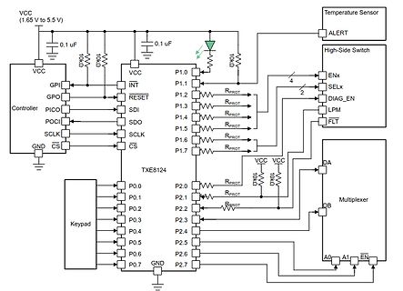
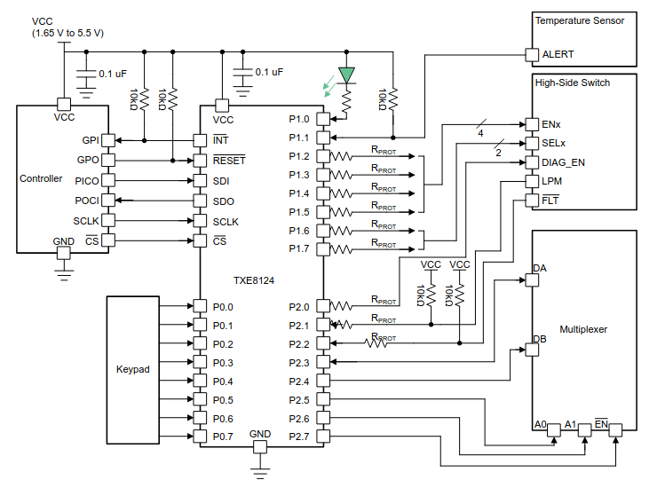
Schaltplan mit Mikrocontroller, Keypad und High-Side Switch
, Controller, PICO, SDI, SDO, SCLK, CS, GND, INT, RESET, TXE8124, Temperature Sensor, ALERT, High-Side Switch, ENx, SELx, DIAG_EN, LPM, FLT, Multiplexer, DA, DB, A0, A1, EN, Keypad, P0.0 bis P0.7, P2.0 bis P2.7
in „Neue Bauteile – kleine Relais, nicht durchbrennende LED-Serienschaltungen und Co“ · Analoge Elektronik und Schaltungstechnik · · Schaltpläne
-
PDF
Aufbau__Signalanlage_KiBa.pdf
→ dieser Impuls setzt gleichzeitig das bistabile Relais und den CD4017 zurück. Warum PNP als High-Side-Schalter: Da beide Minuspole des Relais dauerhaft an Masse liegen, kann die Ansteuerung nicht low-side (über GND) erfolgen. Der Treiber muss stattdessen den Pluspol der jeweiligen Spule pulsförmig auf
in „Lichtschranken-Rundenzähler (12V).“ · Mikrocontroller und Digitale Elektronik ·
-
PDF
BL8028_V1.13_en.pdf
BL8028 BLOCK DIAGRAM DETAILED DESCRIPTION TheBL8028high-efficiencyswitchingregulatorisa internal high-side P-channel MOSFET turns off, small, simple, DC-to-DC step-down converter andtheinternallow-sideN-channelMOSFETturns capableofdelivering upto1.5A ofoutput current. on. The inductor releases the stored
in „Küchenwaage ohne Funktion“ · Mikrocontroller und Digitale Elektronik ·
-
Bild
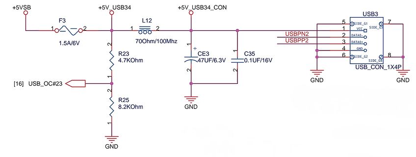
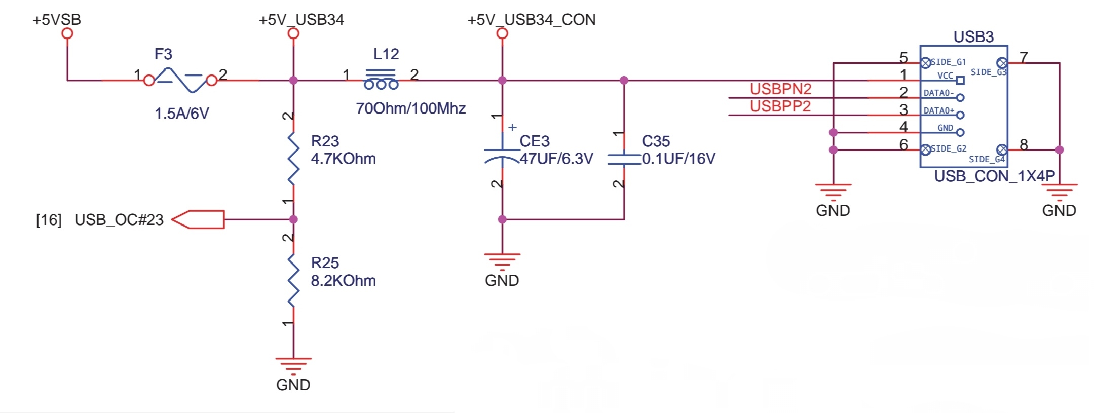
Schaltplan einer USB-Stromversorgung
5V_USB34_CON, R23, 4.7Kohm, CE3, 47UF/6.3V, C35, 0.1UF/16V, USB3, USBPN2, DATA-, DATA+, USBPP2, GND, SIDE_G1, SIDE_G3, SIDE_G2, SIDE_G4, USB_CON_1X4P, [16] USB_OC#23, R25, 8.2Kohm
in „USB-A Shield und Ground verbinden?“ · HF, Funk und Felder · · Schaltpläne
-
PDF
E461201_BA_Rev17_Touch-it_XELO.pdf
......................................................................11 2.3 Interfaces Connector Side (CPU T56N).....................................................................................................12 2.4 Interfaces Connector Side (CPU GX-415GA / i5-4300U).............................
-
PDF
STK625-728.pdf
possible.(Hi Active). • Single power supply drive is possible through the use of a built-in upper-side power-supply bootstrap circuit (Needs external capacitors). • Built-in simultaneous upper/lower ON prevention circuit to prevent arm shorting through simultaneous ON input for the upper and lower side
in „KI gefuehrte Fehlersuche an Waschmaschine Panasonic NA-168VG3“ · Analoge Elektronik und Schaltungstechnik ·
-
PDF
info-uiir2156.pdf
measured under board mounted and still air conditions. Symbol Definition Min. Max. Units VB High side floating supply voltage -0.3 625 VS High side floating supply offset voltage VB- 25 VB+ 0.3 V High side floating output voltage V - 0.3 V + 0.3 V HO S B VLO Low side output voltage -0.3 V CC+ 0.3 IOMAX
in „Leuchtstoffröhren Vorschaltgerät 24V Reparatur-Tipp gesucht“ · Fahrzeugelektronik ·
-
Bild
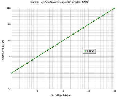
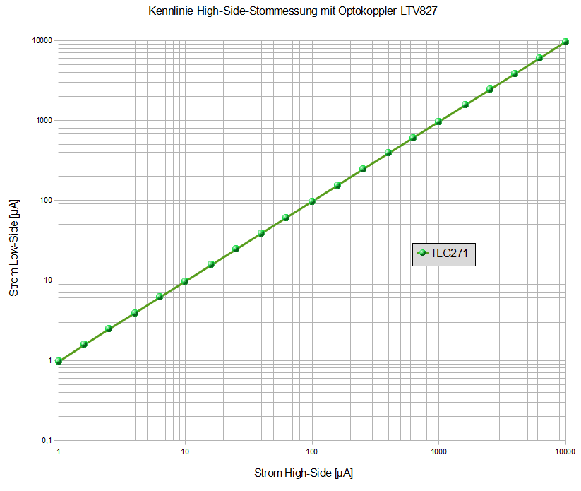
Kennlinie High-Side-Strommessung mit Optokoppler LTV827
Kennlinie High-Side-Strommessung mit Optokoppler LTV827 10000 1000 100 10 1 0,1 Strom Low-Side [µA] Strom High-Side [µA] TLC271
in „Isolierte Spannungsversorgung“ · Analoge Elektronik und Schaltungstechnik · · Diagramme
-
Bild
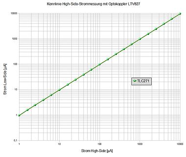
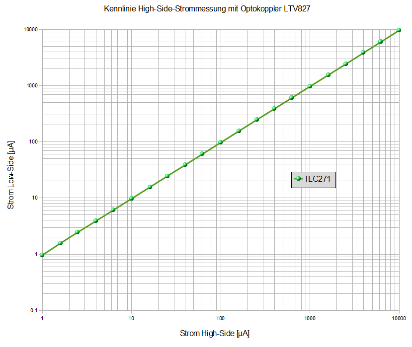
Kennlinie High-Side-Strommessung mit Optokoppler LTV827
Kennlinie High-Side-Strommessung mit Optokoppler LTV827 10000 1000 100 10 1 0,1 Strom Low-Side [µA] 1 10 100 1000 10000 Strom High-Side [µA] TLC271
in „Lineare High-Side-Strommessung mit Optokopplern“ · Analoge Elektronik und Schaltungstechnik · · Diagramme
-
PDF
JW1501ABr0.4_C371169.pdf
JW1501A/B Multi-Mode Primary-Side Regulation (PSR) Parameters Subject to Change Without Notice DESCRIPTION FEATURES JW1501A/B is a high performance Primary Side ● Integrated with 650V MOSFET Regulation (PSR) power switch with high ●
in „SNT Gartenbeleuchtung defekt, pulst aber“ · Analoge Elektronik und Schaltungstechnik ·
-
PDF
I2C_Wandler_an97055.pdf
may have a vast range, depending on the used MOS-FET, e.g. down to 2 Volt at the “Lower voltage” side and up to 10 Volt or more at the “Higher voltage” side of the level shifter. An additional function of the level shifter is that it can isolate a powered-down section in a bus system, without obstructing
in „3.3 Volt vs 5 Volt“ · Mikrocontroller und Digitale Elektronik ·
-
PDF
I2C_Wandler_an97055.pdf
may have a vast range, depending on the used MOS-FET, e.g. down to 2 Volt at the “Lower voltage” side and up to 10 Volt or more at the “Higher voltage” side of the level shifter. An additional function of the level shifter is that it can isolate a powered-down section in a bus system, without obstructing
in „BSS138 vs 2N7002“ · Mikrocontroller und Digitale Elektronik ·
-
Datei
main.py
args, **kwargs) self.btn = T.Button(self, text=f'Name_{index}', command=self.onclick) self.btn.pack(side=T.TOP) def onclick(self, event=None): print('%s called on %s'%(event, self.index)) class MainWin(T.Tk): def __init__(self, *args, **kwargs): super().__init__(*args, **kwargs) self.btns = [BtnFrame(self, i, *args, **kwargs) for i in range(5)] for btn in self.btns: btn.pack(side=T.TOP) self.btnExit = T.Button(self, text='Exit', command=self.destroy) self.btnExit.pack(side=T.BOTTOM) if __name__ == '__main__': MainWin().mainloop()
in „Kopien von tkinter-Frames erstellen und auswerten (python)“ · Softwareentwicklung ·
-
Bild
Schaltplan und Diagramme eines Drucksensors
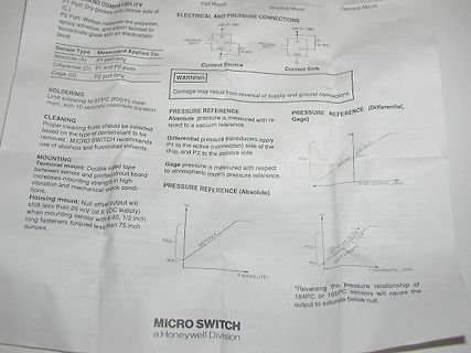
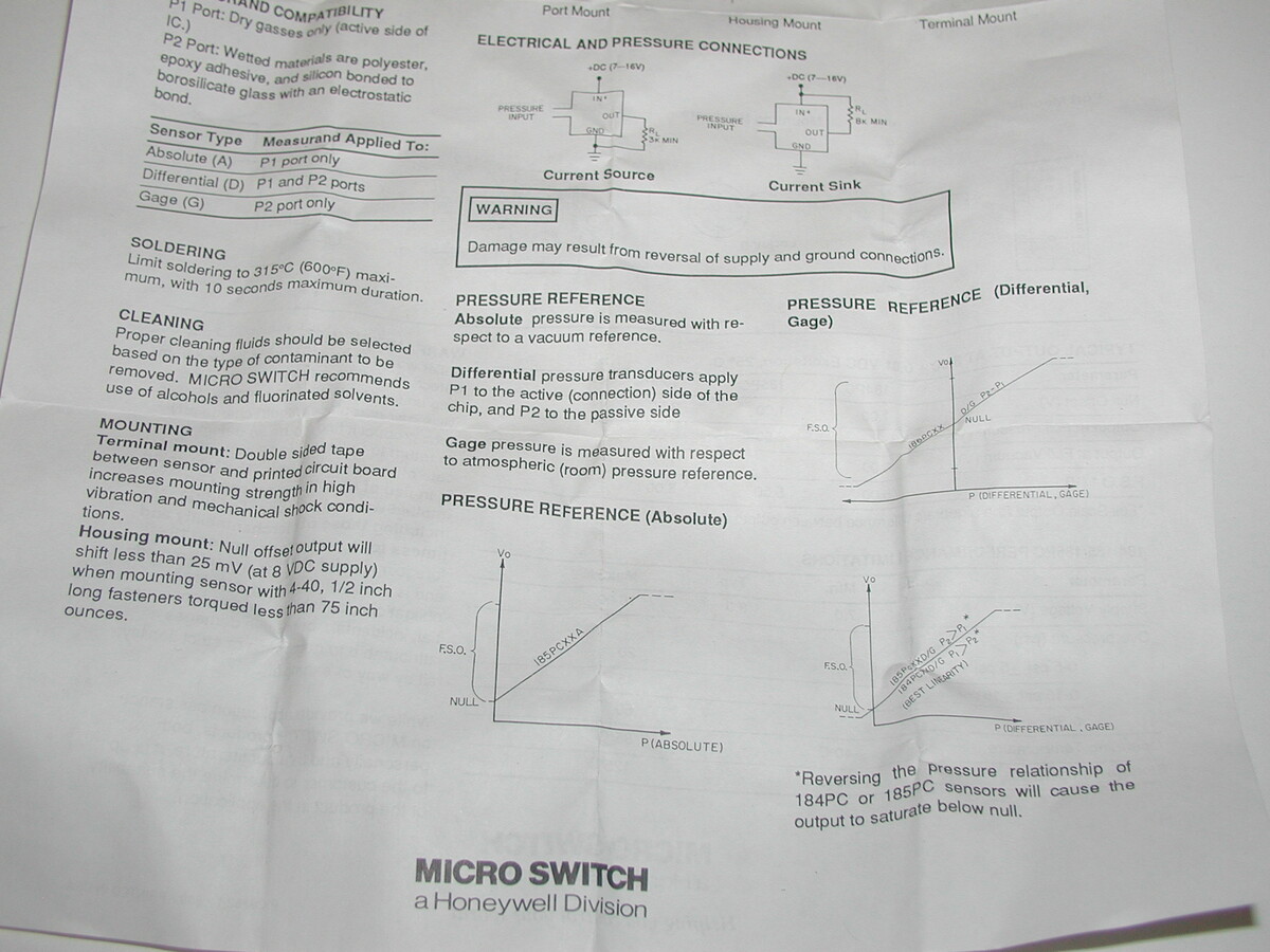
PORT AND COMPATIBILITY P1: Port: Dry gases (only active side of (C.) P2: Port: Wetted materials are polyester, epoxy adhesive, and silicon bonded to a borosilicate glass with an electrostatic bond. ELECTRICAL AND PRESSURE CONNECTIONS PRESSURE INPUT PRESSURE INPUT
in „[VS] verschenke Differential Drucksensor 186PC05DT, +/- 5,0 psi“ · Markt · · Screenshots
-
PDF
Modbus_Messaging_Implementation_Guide_V1_0b.pdf
Client to initiate a transaction, A MODBUS Indication is the Request message received on the Server side, A MODBUS Response is the Response message sent by the Server, A MODBUS Confirmation is the Response Message received on the Client side The MODBUS messaging services (Client / Server Model) are used
in „Modbus RTU Terminal, Freeware Programm“ · Mikrocontroller und Digitale Elektronik ·
-
Bild
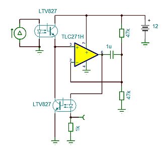
Schaltplan mit Operationsverstärker und Optokopplern
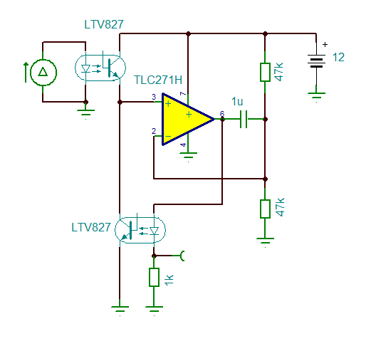
LTV827 TLC271H 1u 47k 12 47k 1k
in „Lineare High-Side-Strommessung mit Optokopplern“ · Analoge Elektronik und Schaltungstechnik · · Schaltpläne
-
PDF
DOC004015493.pdf
CN1 2 6 3 HS3 7 8 FS2 CN2 CN901 M2 CN901 LED 4 -ψ 1234 5 117 35 127 PS/ON 5mA(max.) GND 4 3 . a m 3 Side View File Name:RPT-160-SPEC 2018-01-12 145W Reliable Triple Output Medical Grade RPT-160 series Enclosed Type: RPT-160(G)-C Case No.247A Unit:mm Side View Side View Side View c Air flow Top View m direction FAN 20.5CFM 5 126 120 6 4-M 5 8 3 3L=4 7 R 1 75 110.5 15.5 Side View 130 5 2 1 3 L= 3 4- 120 6 5 0 Bottom View File Name:RPT-160-SPEC 2018-01-12 145W Reliable Triple Output Medical Grade RPT-160 series ※ Mounting Instruction Hole No. Recommended Screw Size MAX.
in „Willtek Schlumberger Stabilock 4031 4032“ · HF, Funk und Felder ·
-
PDF
TJA1020.pdf
between pin INH or BAT on period of time (tNWAKE ) this will also result in a local wake-up. one side and pin LIN on the other side (see Fig.7). A falling edge at pin LIN followed by a LOW level Being in the sleep or standby mode, the TJA1020 enters maintained for a certain time period (t ) and a rising
in „[S] MCP2004 LIN Tranceiver oder andere gesucht“ · Markt ·
-
PDF
3RM13023AA04_datasheet_en.pdf
snap-on mounting onto 35 mm DIN rail height 100 mm width 22.5 mm depth 141.6 mm required spacing ● with side-by-side mounting — forwards 0 mm — backwards 0 mm 3RM13023AA04 9/23/2025 Subject to change without notice Page 3/6 © Copyright Siemens — upwards 50 mm — downwards 50 mm — at the side 0 mm ● for grounded parts — forwards 0 mm — backwards 0 mm — upwards 50 mm — at the side 3.5 mm — downwards 50 mm Ambient conditions installation altitude at height above sea level maximum 4 000 m; For derating see manual ambient temperature ● during operation -25 ... +60 °C ● during storage
-
PDF
C17410452.pdf
------------------------------------------------------- 21 11.1.6 Peripheral Circuit of Secondary-side Shunt Regulator------------------------------ 21 11.1.7 Transformer---------------------------------------------------------------------------------- 21 11.2 PCB Trace Layout and Component Placement
in „Test in der Schaltung STR3A400“ · Analoge Elektronik und Schaltungstechnik ·
-
PDF
manual_en_2015-10-27.pdf
pull forward will gentle rocking (B) Directional Switch – Lever has eight contact motion from back side of panel easing switch out. positions and will operate in horizontal, vertical, and Install new switch and secure using clip retainer on in four intermediate directions. back side of control panel.
in „LED Ersatz für Sealed Beam H9405 gesucht“ · Fahrzeugelektronik ·
-
PDF
PMT_handbook_v4E.pdf
hysteresis. PMT Light hysteresis HL (%) Voltage hysteresis Hv (%) Tube diameter (mm) R6350 0.8 3.0 13mm side-on R11568 0.5 1.0 28mm side-on R928Voltage hysteresis 0.5 1.0 28mm side-on R12421ɹɹ 0.3 1.0 13mm head-on R6095 0.4 2.0 28mm head-on R1306 0.07 0.06 52mm head-on Table 4-5:Typical hysteresis data for
in „Suche nach geeignetem OpAmp als Impedanzwandler“ · Analoge Elektronik und Schaltungstechnik ·
-
PDF
3265fa.pdf
(5mm × 3mm) (Reference LTC DWG # 05-08-1955 Rev Ø) 0.65 ±0.05 3.50 ±0.05 1.65 ±0.05 2.20 ±0.05 (2 SIDES) PACKAGE OUTLINE 0.25 ± 0.05 0.50 BSC 4.40 ±0.05 (2 SIDES) RECOMMENDED SOLDER PAD PITCH AND DIMENSIONS APPLY SOLDER MASK TO AREAS THAT ARE NOT SOLDERED R = 0.115 5.00 ±0.10 TYP 0.40 ±0.10 (2 SIDES) 10 18 R = 0.20 TYP 3.00 ±0.10 1.65 ±0.10 (2 SIDES) (2 SIDES) PIN 1 PIN 1 TOP MARK NOTCH (SEE NOTE 6) (DHC18) DFN 0713 REV Ø 9 1 0.25 ±0.05 0.200 REF 0.75 ±0.05 0.50 BSC 4.40 ±0.10 0.00 – 0.05 (2 SIDES) BOTTOM VIEW—EXPOSED PAD NOTE: 1. DRAWING PROPOSED
in „einfache, kostengünstige Erzeugung einer symmetrischen Spannungsversorgung bei geringer Leistung“ · Analoge Elektronik und Schaltungstechnik ·
-
PDF
Platine_Muster__40x15.pdf
40 10 7,5 5 17,5 2,5 2,5 15 5 Front Side 2,5 2,5 Back Side
-
Bild
Grafik eines Wireless-Tag Moduls mit Stamp-Hole Design
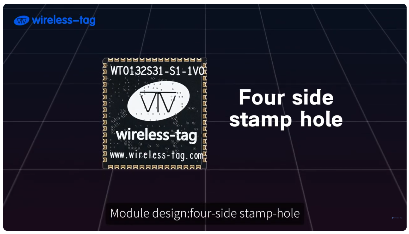
wireless-tag WT0132S31-S1-1V0 Four side stamp hole Module design:four-side stamp-hole www.wireless-tag.com
in „ESP32-S31-Module verfügbar, WiFi HaLow am Vormarsch, uptonitische Quartalszahlen uvam“ · Mikrocontroller und Digitale Elektronik · · Screenshots
-
Bild
Werbeständer für Versaflow Five Selektives Löten
Produce Soldering applications for high flexibility and high throughput independently of each other side by side. Board sizes up to 685 mm. CAD expert mode. High Five for Ultimate Selective Soldering.
in „Productronica – KI, Werkzeuge, Löttechnik und mehr“ · Mikrocontroller und Digitale Elektronik · · Fotos
-
Bild
Pinbelegungstabelle RS-232 Verbindung
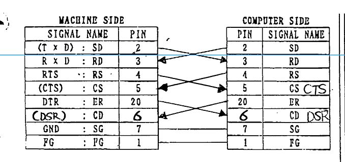
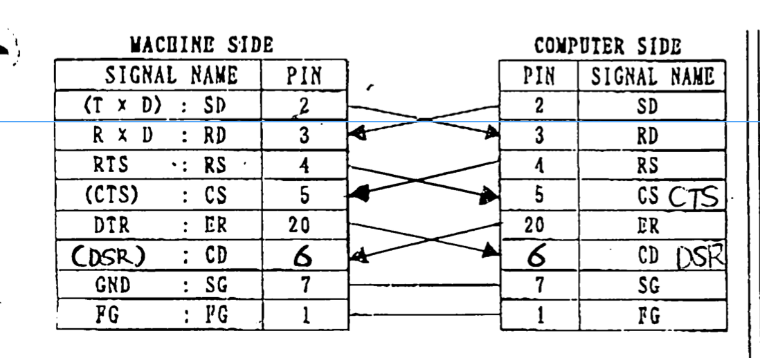
MACHINE SIDE SIGNAL NAME PIN (T x D) : SD 2 R x D : RD 3 RTS : RS 4 (CTS) : CS 5 DTR : ER 20 (DSR) : CD 6 GND : SG 7 FG : FG 1 COMPUTER SIDE PIN SIGNAL NAME 2 SD 3 RD 4 RS 5 CS CTS 20 ER 6 CD DSR 7 SG 1 FG
in „RS32 Kabel für alte Stickmaschine“ · PC Hard- und Software · · Diagramme
-
PDF
1540fb.pdf
R = 0.125 0.40 ±0.10 TYP 5 8 0.70 ±0.05 3.5 ±0.05 1.65 ±0.05 3.00 ±0.10 1.65 ±0.10 2.10 ±0.05 (2 SIDES) (4 SIDES) (2 SIDES) PIN 1 TOP MARK PACKAGE (NOTE 6) OUTLINE (DD8) DFN 0509 REV C 4 1 0.25 ±0.05 0.200 REF 0.75 ±0.05 0.25 ±0.05 0.50 0.50 BSC BSC 2.38 ±0.10 2.38 ±0.05 0.00 – 0.05 BOTTOM VIEW—EXPOSED
in „Komparator Aufbau - diskret oder über µC?“ · Mikrocontroller und Digitale Elektronik ·
-
Bild
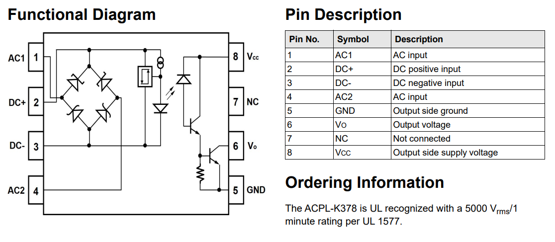
Funktionsdiagramm und Pinbelegung eines Optokopplers
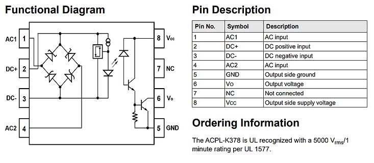
Description 1 AC1 AC input 2 DC+ DC positive input 3 DC- DC negative input 4 AC2 AC input 5 GND Output side ground 6 Vo Output voltage 7 NC Not connected 8 Vcc Output side supply voltage Ordering Information The ACPL-K378 is UL recognized with a 5000 Vrms/1 minute rating per UL 1577.

in „Neue Bauteile: MCX W72, RF-Absicherungsbauteile und intelligentes Hühnerfutter“ · Mikrocontroller und Digitale Elektronik · · Screenshots