
-
PDF
TC4420.pdf
TC4420/TC4429 6A High-Speed MOSFET Drivers Features General Description • Latch-Up Protected: Will Withstand >1.5A The TC4420/TC4429 are 6A (peak), single-output Reverse Output Current MOSFET drivers. The TC4429 is an inverting driver
in „Peltier-Driver Flyback-Diode“ · Mikrocontroller und Digitale Elektronik ·
-
PDF
TC4426.pdf
M TC4426/TC4427/TC4428 1.5A Dual High-Speed Power MOSFET Drivers Features General Description • High Peak Output Current – 1.5A The TC4426/TC4427/TC4428 are improved versions of the earlier TC426/TC427/TC428 family of MOSFET • Wide Input Supply Voltage Operating
in „Mosfet Treiber TC4426 + IRF IRF3205S (Ersatz gesucht)“ · Analoge Elektronik und Schaltungstechnik ·
-
PDF
IRLR7843C.pdf
PD-96058 IRLR7843CPbF IRLU7843CPbF ® Applications HEXFET Power MOSFET l High Frequency Synchronous Buck V DSS R DS(on) max Qg Converters for Computer Processor Power 30V 3.3m : 34nC l High Frequency Isolated DC-DC Converters with Synchronous Rectification for Telecom
in „H-Brücke - 30A - MOSFET“ · Analoge Elektronik und Schaltungstechnik ·
-
PDF
irlr3717.pdf
PD - 94718B IRLR3717 IRLU3717 Applications HEXFET Power MOSFET l High Frequency Synchronous Buck Converters for Computer Processor Power V DSS R DS(on) max Qg l High Frequency Isolated DC-DC 20V 4.0m : 21nC Converters with Synchronous Rectification for Telecom
-
PDF
2210280930_Diodes-Incorporated-AP63300WU-7_C2158012.pdf
VIEW wide input voltage range of 3.8V to 32V. The device fully integrates a 75mΩ high-side power MOSFET and a 40mΩ low-side power MOSFET to provide high-efficiency step-down DC-DC conversion. FB 1 6 BST The AP63300/AP63301 device is easily used by minimizing the external component count due to its adoption
in „Step-Down-Wandler pfeift sehr laut, was tun?“ · Digitale Signalverarbeitung / DSP / Machine Learning ·
-
PDF
AND9674-D.PDF
current during QG (eq. 20) switching is I ): SINKw 1.5 SW, OFF G Q G where: IG.AV.SW+ T (eq. 16) Q = MOSFET gate charge at V = V ; sw_on ń off G GS DD 2. The maximum gate charge, Q , is read from the tSW_ON/OFF = MOSFET switch turn−on / turn−off time; G and 1.5 = empirically determined factor (influenced
in „Bootstrap Kondensator richtig wählen“ · Analoge Elektronik und Schaltungstechnik ·
-
PDF
WebenchReportsServlet.pdf
dissipation 25. L Pd 796.875 m W Power Inductor power dissipation 26. M1 Pd 858.692 m W Power M1 MOSFET total power dissipation 27. M1 PdCond 138.815 m W Power M1 MOSFET conduction losses 28. M1 PdSw 719.877 m W Power M1 MOSFET switching losses 29. M2 Pd 319.225 m W Power M2 MOSFET total power dissipation 30. M2 PdCond 163.551 m W Power M2 MOSFET conduction losses 31. M2 PdSw 155.674 m W Power M2 MOSFET switching losses Copyright © 2012, Texas Instruments Incorporated 2 ti.com/webench WEBENCH ® Design Report LM3150MH : LM3150MH 21.0V-32.0V
in „LM3150 zu geringe Ausgangsspannung“ · Analoge Elektronik und Schaltungstechnik ·
-
PDF
JSM6333C.pdf
JSM6333C N&P-Channel Complementary Power MOSFET Product Summary ● VDS 30V ● RDDS(ON)at GS=10V) <95mohm ● R DS(ON)at GS=4.5V) <150mohm PMOS ● IDS -2.5A ● R DS(ON)at GS=-10V) <220mohm ● R DS(ON)at GS=-4.5V) ● 100% ▽V DSTested r General Description
in „Identifizierung Bauteil“ · Analoge Elektronik und Schaltungstechnik ·
-
PDF
270247_1.pdf
AF4407P P-Channel 30-V (D-S) MOSFET Features General Description -Low rDS(on)rovides Higher Efficiency and Extends These miniature surface mount MOSFETs utilize Battery Life High Cell Density process. Low r DS(on)assures -Miniature SO
in „Suche alternative zu Mosfet“ · Analoge Elektronik und Schaltungstechnik ·
-
PDF
sepic-wanlder.pdf
input voltage. The ripple current flowing in equal value inductors L1 and L2 is given by: Power MOSFET Selection The parameters governing the selection of the MOSFET are the minimum threshold voltage V , the on-resistance R th(min) DS The inductor value is calculated by: (ON),gate-drainchargeQ GD,andthemaximumdraintosource
in „Sepic-Wandler“ · Analoge Elektronik und Schaltungstechnik ·
-
PDF
irl7833.pdf
PD-94668B IRL7833 IRL7833S IRL7833L ® Applications HEXFET Power MOSFET l High Frequency Synchronous Buck V R max Qg Converters for Computer Processor Power DSS DS(on) l High Frequency Isolated DC-DC 30V 3.8m : 32nC Converters with Synchronous Rectification for Telecom
in „Beschaltung Mosfet für Brushless-Regler“ · Analoge Elektronik und Schaltungstechnik ·
-
PDF
PSMN3R7-100BSE.pdf
PSMN3R7-100BSE N-channel 100 V, 3.95 mΩ, standard level MOSFET in D2PAK 3 September 2018 Product data sheet 1. General description Standard level gate drive N-channel enhancement mode MOSFET in a D2PAK package qualified to 175 °C. Part of Nexperia's "NextPower
in „Mysteriöser Mosfet-Tod und der Spirito-Effekt“ · Analoge Elektronik und Schaltungstechnik ·
-
PDF
LTC3824fg.pdf
SS 5μA 3824fg 8 LTC3824 applications information Inductor Selection The power dissipated by the MOSFET when the LTC3824 is in continuous mode is given by : The maximuminductor current is determined by : V V IRIPPLE P = OUT+ D (I ) (1+δ)R IL(MAX) =IOUT(MAX) + MOSFET V IN D OUT DS(ON) 2 (VIN V OUT )•D
in „DC/DC Wandler Vin 15-50V, Vout 12V 9A!“ · Analoge Elektronik und Schaltungstechnik ·
-
PDF
mp1584.pdf
for battery powered cycle starts. If, in one PWM period, the current applications. in the power MOSFET does not reach the COMP set current value, the power MOSFET remains on, saving a turn-off operation. MP1584 Rev. 1.0 www.MonolithicPower.com 7 8/8/2011 MPS Proprietary Information. Unauthorized Photocopy
in „Spannungsregelung mit MP1584 und MP2307“ · Mikrocontroller und Digitale Elektronik ·
-
PDF
MP1584.pdf
for battery powered cycle starts. If, in one PWM period, the current applications. in the power MOSFET does not reach the COMP set current value, the power MOSFET remains on, saving a turn-off operation. MP1584 Rev. 1.0 www.MonolithicPower.com 7 8/8/2011 MPS Proprietary Information. Unauthorized Photocopy
-
PDF
mp1584.pdf
for battery powered cycle starts. If, in one PWM period, the current applications. in the power MOSFET does not reach the COMP set current value, the power MOSFET remains on, saving a turn-off operation. MP1584 Rev. 1.0 www.MonolithicPower.com 7 8/8/2011 MPS Proprietary Information. Unauthorized Photocopy
in „Step Down - Stabil 5V 3A“ · Analoge Elektronik und Schaltungstechnik ·
-
PDF
mp1584.pdf
for battery powered cycle starts. If, in one PWM period, the current applications. in the power MOSFET does not reach the COMP set current value, the power MOSFET remains on, saving a turn-off operation. MP1584 Rev. 1.0 www.MonolithicPower.com 7 8/8/2011 MPS Proprietary Information. Unauthorized Photocopy
in „Empfehlung Step Down Converter IC“ · Analoge Elektronik und Schaltungstechnik ·
-
PDF
C17410452.pdf
Off-Line PWM Controllers with Integrated Power MOSFET STR3A400 Series Data Sheet Description Package The STR3A400 series are power ICs for switching DIP8 power supplies, incorporating a MOSFET and a current mode PWM controller IC. The low standby power
in „Test in der Schaltung STR3A400“ · Analoge Elektronik und Schaltungstechnik ·
-
PDF
PanasonicPhotomosRelayPSpiceSimulationofPhotoMOSRelays.pdf
least 0.4 mm away. The nonlinear source is used for driving the gates of With the help of a control MOSFET, this two source-coupled DMOSFET providing bi- photoelectric voltage drives the gates of two directional switching capability. The model of the source-coupled DMOSFET. Hence the output of the DMOSFET contains a simple MOSFET, capacitors, relay is controlled. resistors, and diodes. Since the PSpice models for MOSFETs were developed for lateral structured field effect transistors, the vertical structure of the DMOSFET transistor
in „Photo_MOS Panasonic AQY212“ · Analoge Elektronik und Schaltungstechnik ·
-
PDF
96151.pdf
V FEATURES AND BENEFITS V FB/OLP . . . . . . . . . –0.5 V to +10 V■ Rugged 650 V Avalanche-Rated MOSFET Package Power Dissipation, PD SimplifiedSurgeAbsorption control (CC × CC(ON)) . . . . . 0.15 W No V Derating Required MOSFET (V DSS × D ). . . . . . 1.35 W ■ Choice of r (3.95 Ω or 6 Ω maximum) total. . . . . . . . . . . . . . . . . . . . 1.5 W DS(on) MOSFET Channel Temp., T . +J50°C ■ Two Operational Modes by Automatic Switching: Internal Frame Temp., TF. . . . +125°C PRC Mode for Normal Operation OpeTat. . . . . . . .-20°C to +125°C† Burst Mode for Stand-By
-
PDF
IRL540N-UMW.pdf
R UMW IRL540N N-Channel Enhancement Mode Power MOSFET Description The UMW IRL540N uses advanced trench technology and design to provide excellenDS(ON)ith low gate charge. It can be used in a wide variety of applications. General Features ● V DS = 100V
in „Problem mit Mosfet IRL540 an 52V, öffnet nicht mehr“ · Analoge Elektronik und Schaltungstechnik ·
-
PDF
MPVD7N65.pdf
MPVD7N65 Power MOSFET SWITCHING REGULATOR APPLICATIONS Features Drain-Source breakdown voltage: BV =650V (Min.) DSS PIN Connection Low gate charge: Q =g0nC (Typ.) D Low drain-source On resistance: R DS(on)1.35 Ω (
in „Unbekannte Bauelemente“ · Analoge Elektronik und Schaltungstechnik ·
-
 Bild
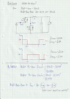
Handschriftliche Berechnung der Verluste in einem Buck-Converter
Buck-Converter Calculate the losses Given: Mosfet1: rDson = 50mΩ Mosfet1 Body-Diode VDF = 1,1 V, RDF = 20mΩ T1 IT1(t) IT2(t) 3A 0,3T T IT1,rms = 1,643A IT1,avg = 0,9A 3A T IT2,rms = 2,5A IT2,avg = 2,1A My Solution: Mosfet1: PT1 = rDson * IT1,rms^2 = 50mΩ * (1,643A)^2 = 0,1349W Mosfet2: PT2 = rDson * IT2,rms^2 = 50mΩ * (2,5A)^2 = 0,315W Mosfet Body-Diode 1: Pbody,1 = VDF * Iavg + RDF * Irms^2 Which current should I use and why?
in „Mosfet Verluste“ · Analoge Elektronik und Schaltungstechnik · · Fotos
-
PDF
en.CD00254735.pdf
function is not used, the pin is left open. Input to the PWM comparator. The current flowing in the MOSFET is sensed through a resistor, the resulting voltage is applied to this pin and compared with an internal reference to determine MOSFET turn-off. The pin is equipped with 150 ns min. blanking time after
in „Flybackcontroller“ · Analoge Elektronik und Schaltungstechnik ·
-
PDF
rd70hvf1c.pdf
Silicon RF Power MOS FET (Discrete) > RD70HVF1C RoHS Compliance, Silicon MOSFET Power Transistor, 175MHz 70W , 520MHz 50W DESCRIPTION OUTLINE DRAWING RD70HVF1C is a MOS FET type transistor specifically designed for VHF/UHF High power amplifiers 25.0±0.3 applications. 7.0±0.5 11.0
in „HF Transistoren“ · Analoge Elektronik und Schaltungstechnik ·
-
PDF
2307271031_Shenzhen-Fuman-Elec-2302P-D_C7495028.pdf
深圳市富满电子集团股份有限公司 SHEN ZHEN FINE MADE ELECTRONICS GROUP CO., LTD. 2302P (文件编号:S&CIC1975) N-Channel Trench Power MOSFET Description General Description Product Summary ● Trench Power LV MOSFET technology ● VDS 20V ● High Power and current handing capability ● ID 3.2A ● RDS(ON)( at VGS=4.5V) <52mohm ● RDS(ON)( at VGS
in „MosFET schaltet PWM Signal nicht“ · Analoge Elektronik und Schaltungstechnik ·
-
PDF
2202251530_Shenzhen-Fuman-Elec-2302P_C2834503.pdf
深圳市富满电子集团股份有限公司 SHEN ZHEN FINE MADE ELECTRONICS GROUP CO., LTD. 2302P (文件编号:S&CIC1975) N-Channel Trench Power MOSFET Description General Description Product Summary ● Trench Power LV MOSFET technology ● VDS 20V ● High Power and current handing capability ● ID 3.2A ● RDS(ON)( at VGS=4.5V) <52mohm ● RDS(ON)( at VGS
in „MosFET schaltet PWM Signal nicht“ · Analoge Elektronik und Schaltungstechnik ·
-
PDF
lm3150.pdf
specified in the electrical characteristics C Omin = 70 / (500 kHz x 1.65 µH) = 169 µF table. The MOSFET gate charge Q is gathered from reading The maximum ESR allowed to prevent over-voltage protec- the V GS vs Qgcurve of the MOSFET datasheet at the V GS = tion during normal operation is: 5V for the high-side, M1, MOSFET and V GS = 6V for the low- side, M2, MOSFET. ESR max = (80 mV x L x Af / ET The Renesas MOSFET RJK0305DPB has a gate charge of A f V OUT / 0.6 without a feed-forward capacitor 10 nC at V = 5V, and
in „LM3150 zu geringe Ausgangsspannung“ · Analoge Elektronik und Schaltungstechnik ·
-
PDF
AN-1484_National.pdf
input voltage. The ripple current flowing in equal value inductors L1 and L2 is given by: Power MOSFET Selection The parameters governing the selection of the MOSFET are the minimum threshold voltage V , the on-resistance R th(min) DS The inductor value is calculated by: (ON),gate-drainchargeQ GD,andthemaximumdraintosource
in „Stepup/-down: Konstante 5V aus 4xMonozelle“ · Analoge Elektronik und Schaltungstechnik ·
-
PDF
AN-1484_National.pdf
input voltage. The ripple current flowing in equal value inductors L1 and L2 is given by: Power MOSFET Selection The parameters governing the selection of the MOSFET are the minimum threshold voltage V , the on-resistance R th(min) DS The inductor value is calculated by: (ON),gate-drainchargeQ GD,andthemaximumdraintosource
in „Längsregler (mit Transistor, Z-Diode, Widerstand)“ · Analoge Elektronik und Schaltungstechnik ·
-
PDF
SEPIC.pdf
input voltage. The ripple current flowing in equal value inductors L1 and L2 is given by: Power MOSFET Selection The parameters governing the selection of the MOSFET are the minimum threshold voltage V , the on-resistance R th(min) DS The inductor value is calculated by: (ON),gate-drainchargeQ GD,andthemaximumdraintosource
in „SEPIC-Mosfet Problem“ · Analoge Elektronik und Schaltungstechnik ·
-
PDF
rd15hvf1-1.pdf
FET ELECTROSTATIC SENSITIVE DEVICE OBSERVE HANDLING PRECAUTIONS RD15HVF1 RoHS Compliance, Silicon MOSFET Power Transistor, 175MHz520MHz,15W DESCRIPTION OUTLINE DRAWING ▯▯▯ʶ▯▯▯ RD15HVF1 is a MOS FET type transistor specifically ▯▯▯ʶ▯▯▯ designed for VHF/UHF High power amplifiers applica ▯ -tions. ▯ ▯▯▯ʶ
in „RD15HVF1 Fake oder nicht Fake das ist hier die Frage ;)“ · Analoge Elektronik und Schaltungstechnik ·
-
PDF
ME8311-Microne.pdf
determined by EA output and current sense signal at pin 4. 4 CS Current sense input pin. Connected to MOSFET current sensing resistor node. HV MOSFET Drain Pin. The Drain pin is connected to the primary lead of the 5,6 DRAIN transformer 7,8 GND Ground Absolute Maximum Ratings Parameter Rating Unit Voltage
in „Schaltkreis 8311A“ · Analoge Elektronik und Schaltungstechnik ·
-
PDF
LNK605etc_linkswitch_ii_family_datasheet-1512164.pdf
operate concurrently in the CC region. The current limit circuit senses the current in the power MOSFET. Constant Voltage (CV) Operation When this current exceeds the internal threshold (I LIMIT the power As the FEEDBACK pin approaches V from the constant current MOSFET is turned off for the remainder
in „Bauknecht Mikrowelle MW59MB Überspannung Spannungswandler“ · Analoge Elektronik und Schaltungstechnik ·
-
PDF
slua149.pdf
part number. NOTE 2: Cout must be low ESR and ESl. NOTE 2: Cout must be low ESR and ESl. NOTE 3: MOSFET ratings and part number. NOTE 3: MOSFET ratings and part number. LOGIC LEVEL gate threshold. LOGIC LEVEL gate threshold. 14 APPLICATION NOTE U-133A OFF-LINE APPLICATIONS: UCC380X OTHER APPLICATIONS
in „Boost Konverter“ · Mikrocontroller und Digitale Elektronik ·
-
PDF
UCC27210.pdf
Matching to 0.9 Ω, thereby allowing for driving large power • Symmetrical Under Voltage Lockout for MOSFETs with minimized switching losses during the transition through the MOSFET’s Miller Plateau. The High-Side and Low-Side Driver input structure is now able to directly handle -10 • All Industry Standard
in „"Pseudo-CMOS Input" oder "TTL Input"“ · Mikrocontroller und Digitale Elektronik ·
-
PDF
semi_eng_apv.pdf
Photovoltaic MOSFET Driver Photovoltaic MOSFET drivers of wide variation FEATURES High-speed switching 6.4 High insulation 8 . 3.9 DIP type: 5,000 Vrms, SOP type: 2,500 Vrms, SSOP type: 1,500 Vrms 8 8 6.4 4.3 4.4 2 .5
in „Gibt es Optokoppler mit Öffner Kontakt?“ · Analoge Elektronik und Schaltungstechnik ·
-
PDF
HMYX_D8575N.pdf
D8575N Datasheet V2.0 30V N-Channel Power MOSFET BV DSS 30 V D8575N D @V GS0V, T =2C°C 60 A RDSON , C =25°C Typ Max 100% ΔV ds TESTED! @V =GSV, I =D5A 6.7 8.0 mΩ 100% UIS TESTED! @V GS.5V, I =D0A 9.5 12 Features ● Super Low Gate Charge ● Green Device
in „Lidl kann auch anders (Lötstation)“ · Mechanik, Gehäuse, Werkzeug ·
-
PDF
MP1584.pdf
for battery powered cycle starts. If, in one PWM period, the current applications. in the power MOSFET does not reach the COMP set current value, the power MOSFET remains on, saving a turn-off operation. MP1584 Rev. 1.0 www.MonolithicPower.com 7 4/7/2009 MPS Proprietary Information. Unauthorized Photocopy
in „COMP PIN MP1584“ · Mikrocontroller und Digitale Elektronik ·
-
PDF
AppNoteRthdetermination.pdf
the thermal resistance R th(CA) of an appli- cation. by Stefan Burges, Christian Arndt If a power MOSFET in used in an application in which high power losses occur (e.g. linear control), it must be ensured that the losses that are dissipated via the heatsink do not lead to thermal overload of the MOSFET
in „Wärmewiderstand Rthg - Rthgk“ · Analoge Elektronik und Schaltungstechnik ·
-
PDF
STK681-332-E.pdf
This reduced DD voltage threshold level is set to 4V (typ.), and the MOSFET gate voltage specification is 5V ±5%. So, a current flow through the output when V DD is rising results in the power stress to the MOSFET due to insufficient gate voltage. To prevent this power stress
in „Thermische Berechnung bei H-Brückentreiber“ · Mikrocontroller und Digitale Elektronik ·
-
PDF
a6252.pdf
flyback converters. They incorporate a primary control and drive circuit with avalanche-rated power MOSFETs. The STR-A6252 featureshigherallowableswitchingcurrentandloweron-resistance. The STR-A6251 is also available for 67 kHz operation. Covering the power range from below 21 watts or 24 watts for a 230
in „FSC Monitor 24" P24-1W schaltet sich immer AUS und AN“ · Analoge Elektronik und Schaltungstechnik ·
-
PDF
irsf3010.pdf
Provisional Data Sheet No.PD-6.0027A IRSF3010 FULLY PROTECTED POWER MOSFET SWITCH General Description: Rating Summary: The IRSF3010 is a three terminal monolithic V ds(clamp) 50 V SMART POWER MOSFET with built in shortcir- cuit, over-temperature, ESD and over-voltage pro-
in „PIC steuert High Side Switch“ · Mikrocontroller und Digitale Elektronik ·
-
PDF
rd15hvf1-1.pdf
< Silicon RF Power MOS FET (Discrete) > RD15HVF1 RoHS Compliance, Silicon MOSFET Power Transistor, 175MHz, 15W DESCRIPTION OUTLINE DRAWING RD15HVF1 is a MOS FET type transistor specifically 9.1+/-0.7 1.3+/-0.4 . designed for VHF/UHF High power amplifiers applica / . -tions. 3 3.6
in „RD15HVF1 Fake oder nicht Fake das ist hier die Frage ;)“ · Analoge Elektronik und Schaltungstechnik ·
-
Datei
Fehlermeldung.txt
N005. This node is used by R8. Instance "m:u1:73": Length shorter than recommended for a level 3 MOSFET. Instance "m:u1:53": Length shorter than recommended for a level 3 MOSFET. Instance "m:u1:55": Length shorter than recommended for a level 3 MOSFET. Instance "m:u1:71": Length shorter than recommended for a level 3 MOSFET. Instance "m:u1:61": Length shorter than recommended for a level 3 MOSFET. Direct Newton iteration for .op point succeeded. Date: Thu Jun 13 09:23:43 2013 Total elapsed time: 0.125 seconds. tnom =
in „LT Spice meldet Fehler/Ignor-Meldung“ · Analoge Elektronik und Schaltungstechnik ·
-
PDF
MC.pdf
MOSFET gate. A 12-V zener clamp insures that the MOSFET gate-source voltage never exceeds 12 V. Series 10-Ω gate resistors tame gate reactance, preventing oscillations and minimizing ringing. The oscillator
in „Ansteuerung BrusslessDC Motor mit MSP430“ · Mikrocontroller und Digitale Elektronik ·
-
PDF
DM6852HR_BDM610010026C.pdf
Output Interface 48 Pin Header Layout (Signals are Paired) Pin Designation Signal Name Sx Source for MOSFET x (ground) Dx Drain for MOSFET x Px +VS supply for MOSFET switch x (required) Figure 7 MosFET Output Schematic DM5852HR/DM6852HR Isolated Digital I/O Module User’s Manual 7 Isolated Input Connector
-
PDF
ncp1200.pdf
the internal IC . 0.16 = 256 mW. If for design reasons this contribution is consumption and the MOSFET’s gate charge, Qg. If we still too high, several solutions exist to diminish it: select a MOSFET like the MTD1N60E, Qg equals 11 nC 1. Use a MOSFET with lower gate charge Qg (max). With a maximum switching
in „NCP1200D6 Schaltnetzteil IC“ · Mikrocontroller und Digitale Elektronik ·
-
PDF
NCP1200.pdf
the internal IC . 0.16 = 256 mW. If for design reasons this contribution is consumption and the MOSFET’s gate charge, Qg. If we still too high, several solutions exist to diminish it: select a MOSFET like the MTD1N60E, Qg equals 11 nC 1. Use a MOSFET with lower gate charge Qg (max). With a maximum switching
in „Datenblatt gesucht DAP07“ · Analoge Elektronik und Schaltungstechnik ·
