Ein Tipp: nimm GROSSBUCHSTABEN nur für konstante Werte wie z.B. Defines. BTW2: diese Zeile [c] if (ADC_CH0_PIN >= (ADCA_CH_PIN_Anzahl + 1)) ... [/c] wäre so leichter les- und verstehbar: [c] if (ADC_CH0_PIN > ADCA_CH_PIN_Anzahl) ... [/c] BTW3: Dieser Kommentar sieht mir recht dubios nach einem hingebastelten Workaround aus: [c] //nur wenn größer Offsetwert um echten O Wert bekommen zu können [/c]
A 15 C C A A 5 0 0 0 0 17 U n s t a b l e 6 0 0 0 0 18 C C A A 7 CCAA 19 0000 8 7743 20 Unstable 9 C96F 21 0000 11 C631 23 CCAAA A 12 0000 24 CCAA RESS YS2 1 @ ®) The next signatures must be megsured on test
signalappliedtogether. ECO L : l y — 5 V —5V -0VCOUNTER B Z mise a | 7 p i ) F “ve GND _ Vapr813 (f] : — 7C E T ]OF T4LS10 2 02 A2 2 iY ! 3 3 A3 sh 2 3 Z E. G pg2_ ? T C eio1 Z) ; | | 15 i [ a Te C E P TL24 a D AT; CO:T i a CET sz Z : D1 01Kz 7BI BIs Z o e s | 3 03e ]83 35 Z i ; PE AcVCC GND VSS GND : 74LSI6I
D0. Ebb oa a oe es g g ei ) 6 . Fig. 2.10. A D C 2 4 4 24, — D I G I T A L S E C T I O N 24.1, A D C interface ‘Theinformationtransport tothisdeviceisby meansofan 12Ccompatibleinterface(see2.4.3.). This A D C interface isactivated by a start conditiosno
accumulated. Internally, this signal will travel down through chain reduce the number of items by half at each level as the shift registers to indicate the last partial sum at each level. N shown in Fig. 4. Each adder takes two inputs and produces Since 2 ▯ L, it is guaranteed that the data arrival interval
example shows plateau characteristic taken at 25 °C along with those obtained at 150 °C, 175 °C, and 200 °C. Because the gain of the photomultiplier tube decreases as the temperature increases, the supply voltage at which the signal appears (corresponding
Christie schrieb im Beitrag #8035192: > Erfahrungswerte haben wir testweise gesammelt: bie -18°C lief der Logger > ohne Watchdog 14 Tage, bei Zimmertemperatur 42. Zum Vergleich: Atmega328, NRF24+-Funkmodul, DS18B20(-Klon) und SHT21 laufen hier seit 1256 Tagen an zwei NiMH AA LSD-Zellen, und
Beitrag #8035212: > Christie schrieb: >> Erfahrungswerte haben wir testweise gesammelt: bie -18°C lief der Logger >> ohne Watchdog 14 Tage, bei Zimmertemperatur 42. > > Zum Vergleich: Atmega328, NRF24+-Funkmodul, DS18B20(-Klon) und SHT21 > laufen hier seit 1256 Tagen an zwei NiMH AA LSD-Zellen
send by MCU, and D2, D3, D4 through pixel internal reshaping amplificat.on to transmit Composition of 24bit Data G7 G6 G5 G4 G3 G2 G1 G0 R7 R6 R5 R4 R3 R2 R1 R0 B7 B6 B5 B4 B3 B2 B1 B0 Note: Data transmit in order of GRB, high bit data at first. TypicalApplication Circuit: No need extra filter capacitor
2.5 Interfaces Connector Side (CPU i5-7300U) USB 4 x USB Host 3.0 (Type A) 1 x USB Host 3.1 (Type C) Ethernet 2 x 1 Gbit Ethernet (Intel I219LM + I211AT) Communication 1 x RS-232 / RS422 / RS-485 (BIOS setting) (RJ50 10P10C) Video 1 x DisplayPort WLAN 1 x 802.11 ac/a/b/g/n 2.4 GHz, 5 GHz, (optional
nmap -sn 192.168.178.0/24 Starting Nmap 7.95 ( https://nmap.org ) at 2026-03-31 13:10 CEST Nmap scan report for aaa (192.168.178.1) Host is up (0.00095s latency). Nmap scan report for bbb (192.168.178.31) Host is up (0.00024s
0.0055s latency). Nmap scan report for 192.168.178.123 Host is up (0.00046s latency). Nmap done: 256 IP addresses (4 hosts up) scanned in 3.02 seconds ping -4 -c 5 192.168.178.123 PING 192.168.178.123 (192.168.178.123) 56(84) bytes of data. 64 bytes from 192.168.178.123: icmp_seq=1 ttl=128 time
IEC 134) VSS = 0V; VSSA= 0V; VSSPA= 0V PARAMETER MIN MAX UNIT Operating temperature range -40 +85 °C Storage temperature range -55 +125 °C Voltage at any I/O and BATpin to SS -0.5 3.6 V Voltage at PAOUT pin to SS -0.5 7.2 V Voltage at any I/O pin tSSV -0.5 V BAT+0.3 V Peak output current port P1x and
nicht davon weg, dass man verstehen muss, was programmiert werden soll. Das ganze für Embedded C und C#
präferierte online-KI zu befragen: den prompt hab ich ähnlich wie hier vorgemacht wurde knapp gehalten: "C-code for ATmega48, RTC @ 32768 Hz, power saving mode, LED blinking at 50ms interval" ich kenn den Atmega48 nicht, bin entfernt vertraut mit den Megas, kann den ausgespuckten Code also nicht wirklich
connected toSS : BS0, BS2, CL, D[7:3], E, R/W#, CS#, D/C#, BGGND, LS Pin internally connected toDD : BS1, CLS VBAT, C1P, C1N, C2P, C2N, FR should be left open. C1, C2: 2.2uF (1) C3: 1.0uF (1) RP: Pull up resistor Voltage at I = V – 3V. For V = 12V, I = 30uA
schrieb: >Ach ja, die 5V ergeben sich daraus, dass das Ganze als >Hardware-Erweiterung an einem C64 laufen soll :) Der C64 hat auch noch 9V~ , daraus kann man mit einen Spannungsverdopplungsgleichrichter auch 18V machen. Siehe hier Seite 84: http://www.homecomputerworld.at/literatur/c64/Hardware_Basteleien_zum_C64_and_C128_(DE).pdf
connected toSS : BS0, BS2, CL, D[7:3], E, R/W#, CS#, D/C#, BGGND, LS Pin internally connected toDD : BS1, CLS VBAT, C1P, C1N, C2P, C2N, FR should be left open. C1, C2: 2.2uF (1) C3: 1.0uF (1) RP: Pull up resistor Voltage at I = V – 3V. For V = 12V, I = 30uA
receives the necessary RTCM data from the base station, maintaining high-precision positioning even at a distance. [/c] ### Microchip PIC32CM * PL10 – mit AVR Dx kompatibler 32-Bitter Microchip möchte Nutzern der AVR Dx-Familie einen Weg zum Umstieg auf 32bit-MCUs geben. Deshab lanciert man sehr
vorgesehene MCX W-Serie gibt es neue Evaluationsboards. Hier eine kleine Liste relevanter SKUs: [c] MCX A173 and A174 => FRDM-MCXA174 MCX A175, A176, A185, A186, A255, A256, A265, and A266 => FRDM-MCXA266 MCX A343 and A344 => FRDM-MCXA344 MCX A355, A356, A365, and A366 =>
9EUR). Beim Bestellen des MC sollte man einen CAN-BUS-Treiber gleich mitbestellen: z. B. Philips PCA82C250. Jedoch auf vorhandene Versorgungsspannungen achten (AT90CAN128 "kann mit" VCC=2,7...5,5V, PCA82C250 lt. Datenblatt für VCC=4,5...5V). CANopen software protocol stacks at Freier CANopen stack: <!-
weil die Anstiegszeit des TX-Signals zu schlecht ist. Freescale MC9S08. D Serie Freescale MC9S12. B, C, D, G und H Serie NXP LPC11CXX. 32-bit ARM Cortex-M0 LPC11C12 16KB flash, 8KB SRAM, 1x C_CAN LPC11C14 32KB flash, 8KB SRAM, 1x C_CAN LPC11C22 16KB flash, 8KB SRAM, 1x C_CAN, on-chip CAN transceiver LPC11C24
boot: ESP-IDF v5.5.2-dirty 2nd stage bootloader I (23) boot: compile time Mar 6 2026 14:55:48 I (24) boot: chip revision: v0.2 I (24) boot: efuse block revision: v0.3 I (27) boot.esp32c6: SPI Speed : 80MHz I (31) boot.esp32c6: SPI Mode : DIO I (35) boot.esp32c6: SPI Flash Size : 2MB
I (253) heap_init: Initializing. RAM available for dynamic allocation: I (259) heap_init: At 40816320 len 000662F0 (408 KiB): RAM I (264) heap_init: At 4087C610 len 00002F54 (11 KiB): RAM I (270) heap_init: At 50000000 len 00003FE8 (15 KiB): RTCRAM I (276) spi_flash: detected chip: generic
above 25⋅C at the following rates: D-14 package at 7.8mW/⋅C D-8 package at 6.3mW/⋅C N-14 package at 11.5mW/⋅C N-8 package at 9.3mW/⋅C April 15, 1992 251 Philips Semiconductors RF Communications Products Product
ab. https://www.spiegel.de/ausland/china-humanoide-roboter-zeigen-kung-fu-im-staatsfernsehen-a-746c4dec-ac7c-437d-ba39-6934f04b1a18
Michael K. schrieb im Beitrag #8017995: > Nur das C3PO nicht Rücken bekommt und dann KK und Staat noch ne Mio > kostet bis er sich zu Tode säuft. Kauft der C3PO auch einen Kleinwagen? Wenn also alle Produktiv leistenden Arbeitende von C3PO Kopien
haben. - 2.2 - CONITEC l H Christian LotDatensysteme G R I P - B e f e h l s s a t z D O P P E L E S C A P E - S E Q U E N Z E N K o n f i g u r a t i o n ESC ESC "0" a Spezifiziere V24-Empfängerbaudrate ESC ESC "l" a Spezifiziere V24-Senderbaudrate ESC ESC "3" a Spezifiziere serielle Tastatur-Baudrate
by MCU, and D2, D3, D4 through pixel internal reshaping amplification to transmit. Composition of 24bit data G7 G6 G5 G4 G3 G2 G1 G0 R7 R6 R5 R4 R3 R2 R1 R0 B7 B6 B5 B4 B3 B2 B1 B0 Note: Data transmit in order of GRB, high bit data at first. 5 / 6 http://www.world-semi.com WS2812D-F8_15mA Intelligent control LED integrated light source Typical application circuit D N 75R L1 C1 4 Din 3 GND 2 VDD 104 1 Dout 5V WS2812D 75R L2 C2 4 3 Din GND 2 VDD 104 1 Dout 5V WS2812D 75R Ln Cn 4 Din 3 GND 2 VDD 104 1 Dout 5V o WS2812D t Modify Records Version № Status Bar Modify Content Summary
±.10] c No. of Dimensions Part Numbers I Positions A B C 15.24 Centerline g 25.10 27.94 30.48 r 24 .988 1.100 1.200 390263-7 e i 28 30.12 33.02 35.56 390263-1 n 1.190 1.300 1.400 E 32 35.20 38.10 40.64 390263
32,768 Hz. The devices are tested not to exceed 35 ppm (parts per million) oscillator frequency error at 25°C, which equates to about ±1.53 minutes per month. With the calibration bits properly set, the accuracy of each M48T58/Y improves to better than +1/–2 ppm at 25°C. The oscillation rate of any crystal
Blitzrate: 1-7 Hz Anzahl der Farben: Farbrad 1: 7 dichroitische + weiß Farbrad 2: 2 Korrekturfilter + weiß 24 mögliche Farbmischungen Maße (LxBxH): 1220 x 440 x 410 mm Gewicht: 38,5 kg Maximale Umgebungstemperatur T : 45° C a Maximale Leuchtentemperatur im Beharrungszustand T :B 95° C Sicherung: F 10 A, 250
Beitrag #8006164: > Den SoC (MEDIATEK MT7621AT) und den DRAM (NANYA NT5CC256M16ER-c) habe Den DRAM gibt es aber nur bis speed grade DDR3L-1866 (933 MHz). Vielleicht wird der Stage 1 bootloader oder dessen Konfig falsch aus
DRAMC calibration failed > > Versucht DDR3L Kalibrierung bei 1200MHz. > Jan schrieb: >> Den SoC (MEDIATEK MT7621AT) und den DRAM (NANYA NT5CC256M16ER-c) habe > > Den DRAM gibt es aber nur bis speed grade DDR3L-1866 (933 MHz). > Vielleicht wird der Stage 1 bootloader oder dessen Konfig falsch
transmitted as a one if the operating voltage has dropped below the low voltage trip point, typically 3.8V at 25°C. This Vsignal is If the supply voltage drops below the low voltage trip transmitted so the receiver can give an indication to the point, the LED output will be toggled at approximately user that
zusammen? Braucht man "einfach nur" eine größere GPU? Welche genau? PS: Da die LLMs ja Probleme mit C und C++ haben - hilft es, den Code erst in Python erstellen und dann nach C / C++ konvertieren zu lassen?
Garnicht so übel. Mein AtMega8535 wollte einfach nicht so richtig bei TWI. Und Fehler in Google eingegeben, KI Antwort: Zitat: "...Nutzen Sie innerhalb von i2c_write für die TWI-Steuerung und die Warteschleife ein anderes
glitch capture (100 ns dual channel) from 5 s/div to 50 s/div Average Number of averages selectable at 8, 64, and 256 Roll Mode At sweep speeds of 200 ms/div and slower, waveform data moves across the display from right to left with no dead time. Display can be either free-running (non-triggered) or triggered
a-high-quality-essential-accessory/ Als neuestes Werkzeug schickt man einen USB-Stick ins Rennen, der mit entweder 128 oder 256 GB Kapazität verfügbar ist: [c] It can sustain a write speed of 75MB/s (128GB variant) or 150MB/s (256GB variant), and our thorough testing has made sure it can handle the demands of real life when
this map peaks at less than 300Mb and is less than 40Mb when the app is idle. [/c] Die im Rahmen der Aussendung mitgelieferte Karte präsentiert sich dann wie in der Abbildung gezeigt. .textContent = data.internal + ' °C'; [/c] aber wenn das '°' Zeichen eingefügt ist, macht der Browser aus mir unerklärlichen
bezüglich des "deep sleep". Hier der Sendercode für einen BME280 und die Ergebnisse der Strommessung. [c] ESP32 sender for BME280 with sleep Measured values on a ESP32 WROOM development board 5V power supply at Vin, red power on board led on 11 mA ESP Sleep (red power LED on) 40 mA ESP ON, Wifi
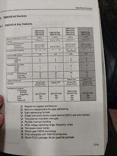
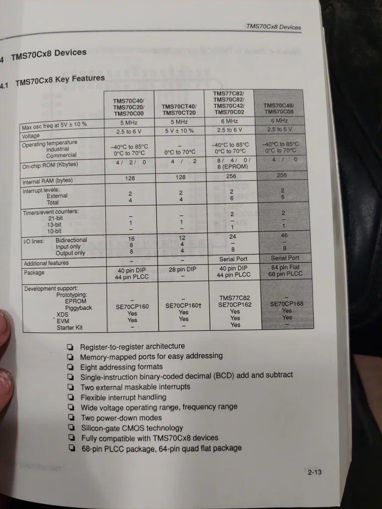
TMS70Cx8 Devices
4.1 TMS70Cx8 Key Features
TMS70C40/TMS70C20/TMS70C00
Max osc freq at 5V ± 10%
5 MHz
Voltage
2.5 to 6 V
Operating temperature
Industrial
Commercial
-40°C to 85°C
0°C to 70°C
TMS70CT40/TMS70CT20
5 MHz
5V ± 10%
128
Internal RAM (bytes)
128
256
256
TMS70C82/TMS70C82/TMS70C42/TMS70C02
6 MHz
2.5 to 6 V
-40°C to 85°C
0°C to 70°C
TMS70C48/TMS70C08
6 MHz
2.5 to 6 V
-40°C to 85°C
0°C to 70°C
Interrupt levels:
External
Total
2
6
2
6
2
6
2
6
I/O lines
just outside the detection band will switch the output > stage on and off at the beat frequency, or the output may pulse > on and off during the turn-on transient. If C3 is too large, turn-on > and turn-off of the output stage will be delayed until the voltage > on C3 passes
outputs. If C3 is too small, > frequencies just outside the detection band will switch the output > stage on and off at the beat frequency, or the output may pulse > on and off during the turn-on transient. If
analog-to-digital converters (ADCs) with up to 17 external channels • 14-bit effective resolution at 250ksps with hardware averaging • One 12-bit 1Msps digital-to-analog converter with integrated output buffer (DAC) • Two zero-drift zero-crossover chopper op-amps (OPA) – 0.5µV/°C drift with chopping
on page 1–24. H The instrument must have had a warm-up period of at least 20 minutes. H The instrument must have had its signal-path-compensation routine last executed after at least a 20 minute warm-up period at
Cascade method: D1 D2 D3 D4 DIN DO DIN DO DIN DO PIX1 PIX2 PIX3 Data transmission method: re se t c o d e > = 5 0 u s re se t c o d e D a ta re fre sh c y c le 1 D a ta re fre sh c y c le 2 se c o n d se c o n d D 1 first 2 4 b 2 4 b ith ird 2 4 b it first 2 4 b2 4 b itth ird 2 4 b it s2 4 b ith ird
at C:/Users/localuser/esp/v5.5.1/esp-idf/components/newlib/src/init.c:18 D (384) cpu_start: calling init function: 0x42001530 on core: 0 --- 0x42001530: __esp_system_init_fn_init_flash at C:/Users/localuser
cpu_start: calling init function: 0x420003a0 on core: 0 --- 0x420003a0: __esp_system_init_fn_init_efuse at C:/Users/localuser/esp/v5.5.1/esp-idf/components/efuse/src/esp_efuse_startup.c:158 D (416) efuse: BLK0 REG2 [24-27], len=4 bits D (420) efuse: BLK0 REG2 [28-31], len=4 bits D (424) efuse: BLK0 REG3
applied to theTVS without operation V Breakdown Voltage -- Maximum voltage that flows though theTVS at a specified test current (I ) BR T V Clamping Voltage -- Peak voltage measured across theTVS at a specified Ippm (peak impulse current) C IR Reverse Leakage Current -- Current measured at V R VF Forward

 Bild
Bild