würdet Ihr empfehlen? So etwas vielleicht: https://cdn-reichelt.de/documents/datenblatt/C300/GC_IC02-24P3XX_DB-EN.pdf Danke https://www.elektrikerwissen.de/strombelastbarkeit-von-steckdosen/
https://www.amazon.de/Ladeschukosteckdose-Wasserdichte-Au%C3%9Fensteckdose-Auto-Hybrid/dp/B0GHR3FHJT/ref=asc_df_B0GHR3FHJT https://www.amazon.de/Legrand-Elektrofahrzeuge-Hybridfahrzeuge-Elektroautos-SAT00194/dp/B07XZM2KQ4/ref=asc_df_B07XZM2KQ4 wenn dir gute Schuko (Gira, Jung) zu windig sind.
Ich sehe immer noch keinen Unterschied. Nur das Manual hat unterschiedliche Nummern: "Manual Ref. 0022381" (A-Version) Erstellt: Mo 03 Jun 2019 09:11:28 +02:00 "Manual Ref. 0029699" (ohne A) Erstellt: Do 03 Jul 2025 11:56:36 +02:00 Also das A wurde später entfernt, das ist die neuere Bezeichnung
Time T 150 250 400 μs SIP CONTROL OUTPUT VOLTAGE(OD&OC) OD Pin Output “H” Voltage V DH VDD-0.1 VDD-0.02 V OD Pin Output “L” Voltage V DL 0.2 0.5 V OC Pin Output “H” Voltage V CH VDD-0.1 VDD-0.02 V OC Pin Output “L” Voltage V 0.2 0.5 V CL 0V BATTERY CHARGE FUNCTION Charger start Available 0V voltage(available
T ES W I T O F FM A I NB E F O R E M O V IP A R T S . 6.2.1 Parts on the PCB - Dismantle PM2534 (refer to section 4.1) - Remove screening 6.2.2 LX- display, window and interconnection rubber - Ddismantle PM2534 (refer to section 4.1) - Remove screening (refer to section 4.2) - Remove front assembly
E Specification of the inputs and outputs of the OQ0063 V [Ravo[sene [ O a r Vss G N DV d d 1 Irs Ref,currentadjustment WithRstheoutputcurrentcanbeadjusted. 17 a L R [16 2 Cs Smoothing Capacitor Smoothing capacitor for the switched currents. 12 . i . 3lie T T 3 Irc |Ref.Common Commonc onnctiono fRsandR
sec vec e e e s e v e s s e e e s s s e e e t e e s s s s e e s e e e2s3 23, Functional section... 02. c eee c e e e e e e e e e c e e e t e e t e e e s e e e s e2n4 2 B N General e e e e e e e e v e r e e r e c t rete et teen een een eee e ns B f 232, Analog section... eevee cece eee eeceeee een eee
higher and lower pulsed light at sufficiently low light levels, the peak currents are Ip a01 Ip res02ctivelyTHBV4_0429EAatio of Ip02Ip 01 proportional to the pulse amplitude; thus Ip02 Ip 014 ................................................................................................ (Eq. 4-13) When
Aussage: Rico schrieb im Beitrag #8034428: > mit drücken sind es 0,02A Demnach hast du dich bis 0,02A "hochgearbeitet". Wenn der Strom nicht weiter steigt, liegt nichts stark niederohmiges vor, somit kann auch nichts warm werden... Das bedeutet: entweder ein anderer
Ersatz zu bekommen wird nicht einfach sein - Gehäuse,Ref Spannung usw. müssen auch stimmen. Hat jemand eine Idee ?
URL https://blog.armbian.com/armbian-q1-2026-technical-milestones-and-the-road-to-embedded-world/?ref=n berichtet man darüber, was in der Welt des quelloffenen Linux-Prozessrechnersystem an Neuigkeiten gibt. Besonders hervorzuheben sind Aktualisierungen der verwendeten Kernelversionen: [c] Kernel
◦ Radxa Rock 4D & ODROID M2: These boards were elevated to the stable support tier within the 26.02 release. • Firmware Updates: U-Boot was bumped to v2026.01 for several platforms. Notably, boot delays on the Orange Pi 5 series were addressed via updated U-Boot candidates (#9450). [/c] ##
revision to include BRD5001A Rev. A07. B03 2020-01-14 New revision to include BRD5001A Rev. A06. B02 2019-12-06 New revision to include BRD5001A Rev. A05. B01 2017-12-19 New revision to include BRD5001A Rev. A04. B00 2015-03-23 New revision to include BRD5001A Rev. A03. A02 2015-02-11 New revision to include BRD5001A Rev. A02. A01 2014-12-18 New revision to include BRD5001A Rev. A01. A00 2014-12-01 Initial Kit Revision. 11.2 Errata There are no known errata at present. silabs.com | Building a more connected world. Rev. 1.0
CS is brought high at any other time, the write operation will 3.2 Read Sequence not be completed. Refer to Figure 3-2 and Figure 3-3 The part is selected by pulling CS low. The 8-bit READ for more detailed illustrations on the byte write instruction with the A8 address bit is transmitted to the sequence
[0x0009 – 0x000E] [0x00] SHAR configures the source hardware address. Ex) In case of “00.08.DC.01.02.03” 0x0009 0x000A 0x000B 0x000C 0x000D 0x000E 0x00 0x08 0xDC 0x01 0x02 0x03 SIPR (Source IP Address Register) [R/W] [0x000F – 0x0012] [0x00] SIPR configures the source IP address. Ex) In case of “192.168.0.2
number of display clocks per row. The value is derived by K = Phase 1 period + Phase 2 period + K =02 + 2 + 99 = 103 at power on reset (i.e. K 0 99) Please refer to Section 6.6 for the details of the “Phase”. Number of multiplex ratio is set by command A8h. The power on reset value is 63 (i.e. 64MUX
number of display clocks per row. The value is derived by K = Phase 1 period + Phase 2 period + K =02 + 2 + 99 = 103 at power on reset (i.e. K 0 99) Please refer to Section 6.6 for the details of the “Phase”. Number of multiplex ratio is set by command A8h. The power on reset value is 63 (i.e. 64MUX
also direkt mit den Ausgängen kurzschließen -LM723 ersetzen durch einfache Spannungsregler oder Ref-Spannungen. -Basisstromquelle eigene Spannungsquelle mit Enable-Eingang (so kann der Basisstrom beim Ausschalten zuerst abgeschaltet werden). -Neuere Opamps sollten nicht schaden, hier am besten
Ich hatte mal vor Jahren dieses Platine neu aufgelegt : https://media.elv.com/file/1996_02_10_netzteilplatine.pdf Grund war etwas Pech und keine Verfügbarkeit mehr über ELV. Meine neue Platine hatte ich bis max. 2A und bis max. 10V ausgelegt. Für die meisten Anwendungen im MC Bereich
CP50 GND 6 bk 4 1 BUS-card GND 7 bk GND A9 GND 8 bk 9 -5V br 10 rd +5V 11 rd +5V +5V 12 rd 454 143/02R bk L1 1 bl N 2 CP1 3 gn/ye 4 6 3 Overview of measuring functions of each test step Test step Functions involved Test as described in section Engine power Acceleration of support roller Roller signals
[0.25] .004-.010 0 - 8 [0.11-0.25] .016-.050 [0.41-1.27] DETAIL A (.041) TYPICAL [1.04] 4214825/C 02/2019 NOTES: 1. Linear dimensions are in inches [millimeters]. Dimensions in parenthesis are for reference only. Controlling dimensions are in inches. Dimensioning and tolerancing per ASME Y14.5M. 2.
ø2 0 2x M1,6 2 deep ø0,2 A A ø0,05 A 0,02 ø10 150 ±10 1 6 ±0,3 2 5x1 25,4 ±0,5 7±0,3 6 1 1525 U ... BRC Option, cable and connection information Example product designation: 1525U012BRC tion e e i tion onne tion e F n tion n t o t t e i tion
user control 0.21 registers, Delete the Section 4.6 Audio Encryption for Privacy , Modify the Vcc 02/23/09 value ;modify the pin FMO back RFO; 0.22 Modify Table 6: match the notes with the parameters; add “at maximal power” 03/18/09 0.23 Add Ordering Information 03/19/09 2 0.24 Modify Figure 11: save
doch nicht, das hat nur einmal funktoniert, dann wieder nicht mehr. Aber ich hab noch was anderes im Ref Manual des 407 gefunden: Peripheral-mode features The OTG_FS interface main features in peripheral-mode are the following: ● 1 bidirectional control endpoint0 ● 3 IN endpoints (EPs) configurable
0x82U /* EP2 for CDC commands First Instance */ #define SECOND_CDC_OUT_EP 0x02 /* EP2 for CDC data OUT Second Instance */ #define SECOND_CDC_IN_EP 0x83 /* EP4 for CDC data IN Second Instance */ #define SECOND_CDC_CMD_EP 0x84 /* EP5
https://www.orientdisplay.com/wp-content/uploads/2021/02/SSD1315.pdf Seite 15
mit zufälligem Inhalt. In diesem Fall musst du im > Quelltext von OLED::display() eine 0x00 auf 0x02 ändern. Die Stelle ist > mit einem Kommentar gekennzeichnet." ist mir auch schon mal begegnet
. g Open Frame r e i Material and Finish: n [2.80]ef. A n Housing — Glass-filled thermoplastic e 0.02Typ. Ref. t Contacts — Beryllium copper [0.50] . w w 0 C B .189 2 [4.80]ef. - 5 2 0 8 : D e A .176 .100 l [4.46]ef. [2.54]yp. c L e s No. of Type/ Dimensions Part u Positions Centerline A B C D Numbers
012 Cl—I 01 013 vcOOuT Cl —2 5 FYI 014 RXI 014100 C1 1 1MHz RX2 CD4060 S T 1 ( X ) - ZENER Rege isp, ref f ST2 II 1C3 12 9 01 I 02 RESET,: : 0 0 n 03 Pt V 04 ST3 05 5T7 +5V bis +15V 06 f out 07 C5 + c C 7 1 c 08 09 010 SIB OCn lOOn 011 k e r jk e r Ik e r 012 Bud 2: Schaltbild der mit dem CD4046 aufgebauten
14 INT OUT RUN/HOLD 4 25 D3 -1.2V COMP IN 5 24 D D, COMP OUT 2 13 +BUFF IN 4 crop V- 6 23 B8(MSB) REF CAP 3 12 +INT IN REFERENCE 7 22 B4 esso REF BYPASS 4 11 -INT IN REF. CAP. 18 21 B2 GND 5 VREF 10 -BUFF IN REF. CAP. 29 20 B1(LSB) erfa REF OUT 6 9 BUFF OUT ANALOG IN 10 19 D5(MSD) ICL8052A/ ANALOG GND
operation can resume rec after CC exceeds V PFD (max). For more information on battery storage life refer to the application note AN1012. 14/33 Doc ID 2412 Rev 8 M48T58, M48T58Y Clock operations 6 Clock operations 6.1 Reading the clock Updates to the TIMEKEEPER registers (see Table 5) should be halted
M48Z02, M48Z12 5 V, 16 kbit (2 Kb x 8) ZEROPOWER® SRAM Datasheet -production data Description The M48Z02/12 ZEROPOWER® RAM is a 2 K x 8 non-volatile static RAM which is pin and function compatible with the
COM0A1)|(0<<COM0A0)|(1<<COM0B1)|(0<<COM0B0)|(1<<WGM01)|(1<<WGM00) ;TCCR0A out TCCR0A, AL ldi AL, (0<<WGM02)|(0<<CS02)|(0<<CS01)|(1<<CS00) ;TCCR0B /1 out TCCR0B, AL clr AL ;kein INT sts TIMSK0, AL ; Counter 2 Mode 3 ldi AL, (1<<COM2A1)|(0<<COM2A0)|(1<<COM2B1)|(0<<COM2B0)|(1<<WGM21)|(1<<WGM20) ;TCCR2A sts TCCR2A
device. Maintenance and service operations are only to be carried out by authorized dealers. Please refer to the instructions under "Installing/Replacing the lamp". Replacing the fuse If the fine-wire fuse of the device fuses, only replace the fuse by a fuse of same type and rating. Before replacing the
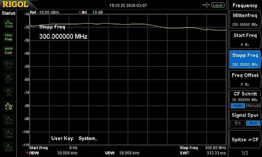
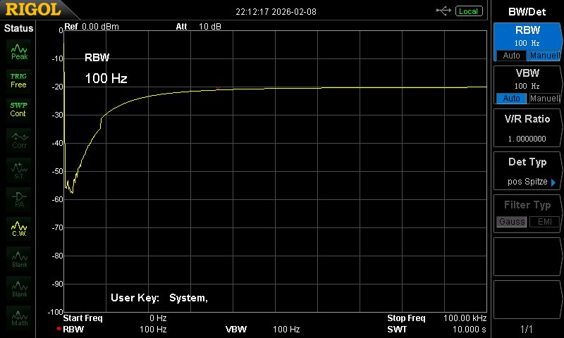
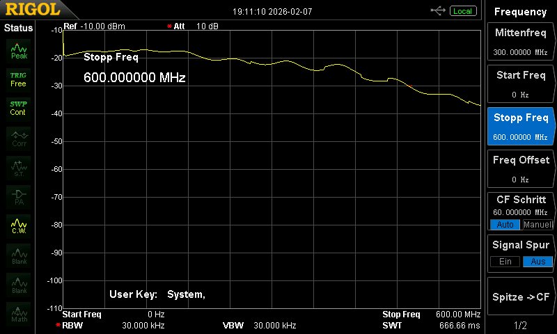
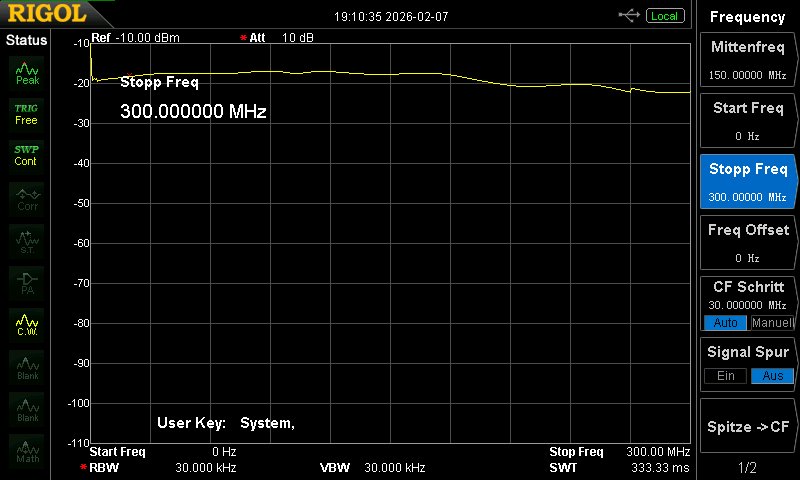
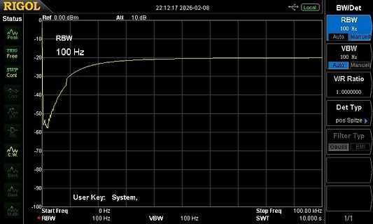
RIGOL 22:12:17 2026-02-08 Local BW/Det Status Ref 0.00 dBm Att 10 dB 100 Hz RBW Peak -10 RBW 100 Hz Auto Manuell -20 TRIG SWP -30 Cont V/R Ratio -40 Corr 1.0000000 Det Typ -50 S.T. pos Spitze -60 PA Gauss EMI -70 C.W. Filter

 Bild
Bild
 Bild
Bild
 Bild
Bild
 Bild
Bild
 Bild
Bild
 Bild
Bild
 Bild
Bild
 Bild
Bild
 Bild
Bild