. TEMPERATURE 0 1.8 t 1.5 t SDA = SCL = CC, V+ = 15.5V 5 5 2 1.6 RW, RH, AND RL ARE FLOATING D D 1.4 1.4 A A ( 1.2 ( N N 1.3 E 1.0 E U U Y 0.8 Y L L 1.2 U 0.6 U S S 0.4 1.1 0.2 SDA = SCL = VCC= 5V, V+ = 15.5V RW, RH, AND RL ARE FLOATING 0 1.0 2.5 3.0 3.5 4.0 4.5 5.0 5.5 -40 -20 0 20 40 60 80 100 SUPPLY
processing toolbox renders efficient designs in short time, a Matlab code that does it is Code 3.1.4 Fsl = 160e6; dm = fdesign.lowpass(‘Fp,Fst,Ap,Asf,20e6,79e6,0.1,105,Fsl); hm = design(dm); b13 = hm.numerator; b13 = b13/(sum(b13) + eps); Fp is the largest passband frequency at which the filter gain
war ich zwar noch nicht, aber die Idee mit dem Gras ausstopfen klingt gut! Merke ich mir. Roland E. schrieb im Beitrag #7390793: > Die Unplattbaren brauchen 3,5-4,5bar. Da kann man auch fast Vollgummi > fahren. 4 bar sollten Fahrradreifen immer haben, auch die normalen "Plattbaren". Erstens fährt
Dann bin ich auf Schwalbe Maraton Plus umgestiegen und hatte viele Jahre Ruhe. Auch jetzt mit dem E-Bike nutze ich Maraton Plus mit 4 Bar und bin sehr zufrieden. An einer Tankstelle: Beim aufpumpen meines Rades auf 4 Bar beobachtet mich ein Motoradfahrer und sagt mit erstauntem Gesicht: Bei Dir
1000 VGS TOP 15V TOP 10V 10V ) 8.0V ) 8.0V t 100 7.0V ( 7.0V n 6.0V n 6.0V r 5.5V r 5.5V u BOTTOM 4.5V u 100 BOTTOM 4.5V e 10 C r r o u - ≤60μs PULSE WIDTH S t 1 t i Tj = 25°C n r r 10 D D ,D 0.1 ,D I I 4.5V 4.5V ≤60μs PULSE WIDTH Tj = 175°C 0.01 1 0.1 1 10 100 1000 0.1 1 10 100 1000 VDS, Drain-to-Source
VC2. The test methods of 4-cell and 3-cell application are as same as 5-cell application. 1. Normal and Sleeping Current Consumption Test circuit 1 (1) Set V1=V2=V3=V4=V5=3.50V, the current flowing to GND is the normal operating
W) Bestückung l Röhre ECC 4 0 l Röhre EB 41 l Stabilisator STV 100/60 Z II l Schmelzeinsatz 0 ,4 DIN 41571 (0,4A ;50x20m m ) l Zwergglimmlampe 220V Abmessungen 315 x 227 x 226 mm (R&S-Normkasten Größe 35) Gewicht 10kg i e c d e
A 1 A 2 A3 bp c D E e H E L Lp Q v w y Z θ 0.3 2.45 0.49 0.32 13.0 7.6 10.65 1.1 1.1 0.9 mm 2.65 0.1 2.25 0.25 0.36 0.23 12.6 7.4 1.27 10.00 1.4 0.4 1.0 0.25 0.25 0.1 0.4 o 8o 0.012 0.096 0.019 0.013 0.51 0.30 0.419 0.043
use d together are placed into the equation . andit is resotv- 155 • N • C ' 2 0 R 1 ~L • C. T 0 6 5 4 P 3 3 3 R R R 0 B I " J - T 7 . 2 " 3 S ~ . c C C s ~ ~ ~ D n ~ - 3 0 e u 3 1 ~ R i ~ i h , r g 4 e T I 2 H g L O F C 0 0 P ' " VHF-COMMUNICATIONS 3184 ed according to the delay time, the following logarithmic
- 2 g t n e I ~ " T s ~ ; a n g c " ; w . , 5 1 p . 4 e m . r . 7 ; 4 , , I : 2 - I j 2 3 c : 1 " " o 9 L 0 . n v l , , M . ~ " s 0 M c 3 l : s i p 3 . C 4 2 9 n h 2 4 l f 4 l y g 4 - ; d w 0 I - a h . r - O e o
device driver, go through the following steps: 1. Ensure that you are logged on as a superuser. 2. Type sam <Enter> at the system prompt to bring up the System Administration Manager (SAM). 3. Choose the Peripheral Devices icon. 4. Choose the Terminals and Modems icon. 5. Select the driver you wish to remove (usually /dev/tty0p0). 6. Make a note of the Hardware Path, which has the format 8/12/4. This path will be needed to install the new driver. 7. Choose the Remove Modem or Remove Terminal command from the Actions menu. 8. Choose Exit (File menu). 9. Choose Exit SAM (File menu). NOTE: To
Development System & Software Data Sheet Multiple Platforms—The MAX+PLUS II software runs on Windows NT3.51or4.0,Windows95,or486-orPentium-basedPCs, and on Sun SPARCstations, HP 9000 Series 700/800, and IBM RISC System/6000 workstations. Full Integration—The MAX+PLUS II software design entry, processing, and
Translation here: some GPIO to spring connector https://dfimg.dfrobot.com/nobody/wiki/79daa2f3c729e78f0580b474fe33a5e3.pdf D13 1 2 3 K2 --> This means we can use a 3V3 transceiver and can be on the same 3V3 powerrail as the ESP. No need to go to 5V C18 PSM712-LF-T7 G5Q-14 DC24 D 1uF D12 D CN4 U14 TVS
im STM-Land ,) Tatsächlich habe ich auch keine Erfahrung mit dem SAMDx (wir nutzen verschiedene SAM4x-Baureihen). 1.) ich kann mir gut vorstellen, dass das setzen der Bits von Studio 7 NICHT funktioniert (Studio 7 nutzen wir aber nicht), da der Vorgang doch einigermassen komplex ist (jedenfalls komplexer
4000 MOQ = Minimum Order Quantity, consisting of 4 packing units. Further E series and intermediate capacitance values on request. Composition of ordering code + = Capacitance tolerance code: *** = Packaging code: K = ±10% 289 = Straight terminals, Ammo
stark erhitzt, fließt dort automatisch weniger Strom. Die Hersteller erlauben das explizit: https://e2e.ti.com/support/logic-group/logic/f/logic-forum/761864/faq-can-i-connect-two-outputs-from-a-cmos-logic-device-together-directly > It is possible to parallel channels of a device to increase drive > strength -- it is just important to ensure that both outputs are always > in the same state. The best way to achieve this is to use two channels > in the same device, and to directly connect the inputs together to > ensure they will always have the same state. Mit deinem 74HCT245
style -07, 1 A types (same dimensions as style -06) Connection style -07, 3 to 20 A types (same dimensions as style -06) Connection style -08, 20 and 30 A types 4 EMC/EMI Products Schaffner Group Datasheets 2016 Dimensions 1
xxxxxxxxxxxxxxxxxxxxxxxxx xxxxxxxxxxxxxxxxxxxx xxx N O r R M d 5 X P u 2 P N t S Y a ADDRESS DATA e P a m U s RX L e SA A0 A1 A2 A3 A4 A5 (1)R/W SO SA D0 D1 D2 D3 D4 D5 D6 D7 SO c C e o t n d u c o r ADDRESS s TX SA A0 A1 A2 A3 A4 A5 (1) R/W SO l f m o R p e v . d MX . n — s 1 o DTRQ 1 7 m 001aak589
// set WDCE to access prescaler WDTCR = 1 << WDP3; // set prescaler bits to 4s WDTCR |= 1 << WDTIE; // enable WDT interrupt interrupts (); // same as sei() sleep_cpu (); // sleep [/c] Und damit schläft der Controller
könnte auch ein ganz trivialer Grund sein: Er toggelt eine LED mit dem Interrupt und dann ist die 4s an und 4s aus und er wollte eigentlich eine Periode von 4s?
BITS C DB23 DB22 DB21 DB20 DB19 DB18 DB17 DB16 DB15 DB14 DB13 DB12 DB1 1 DB10 DB9 DB8 DB7 DB6 DB5 DB4 DB3 DB2 DB1 DB0 X X G1 B13 B12 B11 B10 B9 B8 B7 B6 B5 B4 B3 B2 B1 X X X X X X C2(0) C1(1) FUNCTION LATCH K - -2 C C E E T R 1 E T RESERVED EN CURRENT CURRENT TIMER COUNTER OD O B R T R MUXOUT E N TE
degraded accuracy can be observed. www.onsemi.com 18 NCP380, NCV380 t S o U D P V D D G N S U t o P 5 2 3 4 S ) + − U s D D N m e G e ( t S n 1 C B D o C V N D e V ] ] G 1 L i : : 3 B c L [ M U n T T 0 r C D J M T 6 T 2 1 C S 1 m 3 S 0 P 1 G S ] ] t r Y x 0x o l S T T H t U U 6 5 4 B n _ _O U C L A T I G R
TLC5940 www.ti.com SLVS515D –DECEMBER 2004–REVISED NOVEMBER 2015 6.7 Typical Characteristics 10−k 4−k 7.68−kΩ TLC5940PWP PowerPAD−Soldered - W TLC5940RHB ) m E − 3−k ( t − 1.92−kΩ R TLC5940NT r n s t s a e 1−k 0.96−kΩ s 2−k e i c 0.64−kΩ − r 0.48−kΩ e TLC5940PWP f 0.38−kΩ w PowerPAD−Unsoldered e P
Moe E. schrieb im Beitrag #7375553: > Ich glaube da ist mein Denkfehler. Woher weiß der FMC welche Bank er > ansteuern muss? Aufgrund der Zieladresse. Moe E. schrieb im Beitrag #7375553: > Oder übergebe
Moe E. schrieb im Beitrag #7375602: > HAL_SDRAM_Write_8b Warum jetzt wieder HAL?
0.1uF 过温::闪烁 5下,灭 2秒,一直循环 D2 LED R8 R2 Q1 JP4 3 6 510Ω C3 2.2K 8050 L 7F S 5 4 G D D 0.1u4 TLP-250 5 E A P X X N T T JP7 JP8 FANCTR RT1 R3 O N W D D D 0 1 17 U T E 死区选择 NTC/10K 200K 9 T R N 3 1 8 TFB 温度传感器 C5 C4 R4 R5 PWMTYP VVVF 2 2 7 0.1uF 16
4.7Ω V2 6 FRQADJ/VFB2 R R M C LCDDI 5 C9 C10 2SA1015 10 NC VB 7 R13 IRF840 R14 IRF840 V Q Q D D 0.1uF10uF/16V R37 +5V S 10uF/16V 2HO 10 10K 10K R E E E S N N L L R36 5.1K 11 VDD 0 VS 6 L1 正弦 220V输出 F 0
Modellpalette – die Fertigung erledigt durch die Bank TSMC im 22nm-Verfahren. 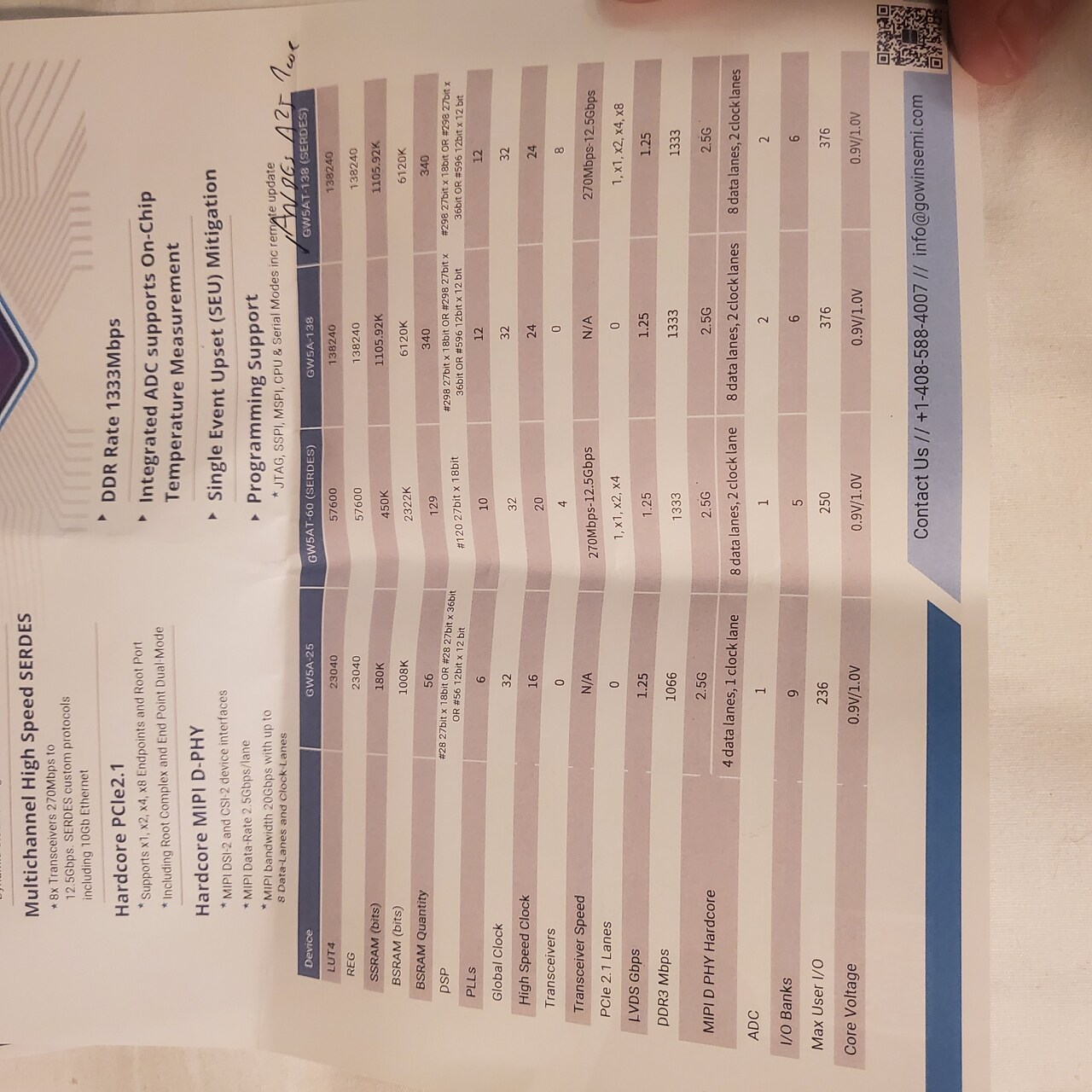 Exklusiv können wir dank CEO Jason Zhu berichten, dass die links gezeigten Modelle G5WA-25 und G5WAT neben dem RISCV-Kern auch einen auf Cortex M4 basierenden Mikrocontroller mitbringen werden
Low-End-Bereich: Renesas mit FPU, Texas Instruments mit „Menschenfreundlichkeit“. Renesas schickt mit dem RA4E2 einen neuen Low-End-Controller ins Rennen, der - das wird vom Standpersonal explizit zugegeben - zur „Bekämpfung“ des STM32C0 vorgesehen ist. Alleinstellungsmerkmal des Cores - mehr Informationen finden
100 ▯ B59451C1130B070 C750 260 360 25 ±25 115 1.0 100 X B59750C0120A070 C751 260 360 50 ±25 115 1.4 120 X B59751C0120A070 C755 560 800 500 ±25 110 1.4 120 X B59755C0115A070 Please read Cautions and warnings and Page 2 of 11 Important notesat the end of this document. Inrush current limiters Leaded
0 1 2 3 4 5 6 7 8 9 A B C D E F WST SECAM 000 AA AA FF FF E7 2E 20 A6 E4 B4 0E 0 7 0 10 0 WST SECAM 010 AA AA FF FF E7 2E 20 A6 E4 B4 0E 0 7 0 10 0 WST PAL B 020 AA AA FF FF 27 2E 20 AB A4 72 10 0 7 0 10 0 WST PAL B 030 AA AA FF FF 27 2E 20 AB A4 72 10 0 7 0 10 0 WST PAL C 040 AA AA FF FF E7 2E 20 22 A4 98 0D 0 0 0 10 0 WST PAL C 050 AA AA FF FF E7 2E 20 22 A4 98 0D 0 0 0 10 0 WST NTSC 060 AA AA FF FF 27 2E 20 23 63 93 0D 0 0 0 10 0
V4 p Power Save E - VDD COMS 2 uO n These are the COM output terminals for the indiBoth terminals output the same signal. S output by both master and slave.e not usWhen in master/slave mode, the same signal
USB cables, and a separate specification for low-speed cables exist. VDD USB_VREGO USB_VREGI 1 µF 4.7 µF USB_VBUSEN EFM32 USB Captive Cable USB_VBUS USB_DP 15 R VBUS D- USB_DM 15 R GND USB_DMPU 4k7 Cable shield USB_ID VSS Figure 2.4. USB Low-speed Device Schematics When designing hardware for a Low-speed
Frank E. schrieb im Beitrag #7363869: > Was ist eigentlich an meiner Frage gleich 4 mal "nicht lesenswert" > (18:21)? Threads nicht kapern, neuen Thread dazu anfangen.
Frank E. schrieb im Beitrag #7363869: > Was ist eigentlich an meiner Frage gleich 4 mal "nicht lesenswert" > (18:21)? Weil man von einem Forum Antworten erwartet und nicht noch mehr Fragen?! Weil
will show PB0 going high for a short period of time at each negative edge zero crossing (See Figure 4 and Figure 5). Figure 4. Screenshoot from Oscilloscope, Mains Input and PB0 Output 4 AVR182 2508B–AVR–01/04 AVR182 Figure 5. Screenshot from Oscilloscope, Mains Input and PB0 Output In a real application
Das Alter ist weitaus weniger als 15 Jahre. Unidentifizierte ICs: SAM_2301: Aufschrift: ADKKU 1D111B3, hängt am I²C. SAM_2302: Aufschrift: 52143A0 1A 1837 AJ6075
Peter N. schrieb im Beitrag #7361029: > SAM_2301: > Aufschrift: ADKKU 1D111B3, hängt am I²C. Neben I²C aber auch an was deutlich schnellerem (differenziell, kapazitiv gekoppelt, vmtl. Impedanzkontrolliert)... > SAM_2302: > Aufschrift
. Allgemein ist das Thema Gf-NE4 halt noch relativ unbekannt und damit sind Unsicherheiten bei den Kunden vorhanden. Wenn eine Gf-NE4 vorhanden ist nutzt eigentlich jeder Anbieter die gerne mit. Hmmm schrieb im Beitrag #7359516:
mal mein kleines Problem, daran hänge ich gerade leider etwas. Auf dem Arduino Due verfügt der SAM3X über erweiterte SPI-Fähigkeiten. Es ist möglich, diese erweiterten Methoden oder die AVR-basierten zu verwenden. Die erweiterte API kann die Pins 4, 10 und 52 für CS verwenden. Soweit ist das
Hallo zusammen, das Problem beim Due ist, dass der verwendete MC SAM3X8E zwar viel kann, aber die üblichen Arduino-Bibliotheken das nicht unterstützen. Verwendet man die Arduino-Biblioithek ist man selbst in der erweiterten SPI-Bibliothek auf die softwaremäßige Ansteuerung
I [N Tj = +105°C T : IE O5.025 i t : p r60 e m u t 5.000 s C o o s V 4.975 C B40 u n e t r b O 4.950 u n C E20 4.925 + 4.900 0 -40 0 40 80 120 0 10 20 30 40 50 Junction Temperature: Tj [°C] Input Voltage: V [V] IN Figure 3. Figure 4. Output Voltage
use d together are placed into the equation . andit is resotv- 155 • N • C ' 2 0 R 1 ~L • C. T 0 6 5 4 P 3 3 3 R R R 0 B I " J - T 7 . 2 " 3 S ~ . c C C s ~ ~ ~ D n ~ - 3 0 e u 3 1 ~ R i ~ i h , r g 4 e T I 2 H g L O F C 0 0 P ' " VHF-COMMUNICATIONS 3184 ed according to the delay time, the following logarithmic
is to obtain a required bannwi dth With a minimum of insertion loss. and Anenuation aIle' ae, = 36 -4 0 dB Upper cu t-ott trequency ' 0= 150 MHz at the same time 10 obta in the requiredauenu a Attenuation at le2 a 2 - 3 6 - 3B dB lion values for out-ot-nnno Signals (ultimate e auenuanon). Table 1: F,
was 11.5 dB with OIP3 = Ql,2: HEC 2SC1252 or 2H5109 with heat sink. Tl,2: wound on F a i r - R i t e 2843002402 balun +42 dBm and NF = 5.7 dB. The individual cores. Each turn i s one pass through BOTH stages had a 4.1-dB NF. The figure h o l e A l i three windings e xat same end. includes measured return
Figure 4. Temperature Coefficient from Figure 6. IGBT Output Characteristics for the Transconductance Curves NGTB15N60S1ETG By graphically determining the currents at gate voltages Figure 6 is one of those curves
V AC V DC % °C J/K s B750 260 360 25 ±25 115 1.0 100 X X B59750B0120A070 B751 260 360 50 ±25 115 1.4 120 X X B59751B0120A070 B752 260 360 80 ±25 115 1.4 120 X X B59752B0120A070 B753 440 620 120 ±25 115 1.4 120 X X B59753B0120A070 B754 440 620 150 ±25 115 1.4 120 X X B59754B0120A070 B755 560 800 500
