-
PDF
AD9235.pdf
Rev. C | Page 31 of 40 AD9235 F 1 0 0 C 0 µ F 3 . 4 0 C 0 +C 1 P 0 µ U D C 1 E N R 2 0 + S 7 D R Y 3 L R P D F D M D E N x N V 1 N A N E A R D 9 0 G V G T 2 C 0 A R G G E 3 5 F I O V R 2 1 S T O 4 0 A S E Ω C C 0 Y W R 0 D B O Y x T 7 µ H S L R A 4 . T C E x L C 0 A T D R C F L A N H 1 E O C C 0 H R T
in „Einstellen eines ADCs“ · Mikrocontroller und Digitale Elektronik ·
-
PDF
datasheet.pdf
# A15 A10 A9 A7 A6 A4 A2 A1 A0 V IH VIL R1, R2, R8, R9 R3, R4 R5, R6, R7 Manufacturer ID: Spansion L L H X X VID X L X L L L 00 X 01h 01h 01h Products A Cycle 1 L L H 22 X 7Eh 7Eh 7Eh 4 Cycle 2 H H L 22 X 0Ch 10h 13h 0 00h (-R4, L L L H X X VID X L X 9 Cycle 3 H H H 22 X 01h bottom boot) 01h 2 01h (-R3, top S boot) Cycle 1 L L H 22 X 7Eh 7Eh 2 Cycle 2 H H L 22 X 1Dh 1Ah 0 L L L H X X VID X L X 00h (-R4, 9 Cycle 3 H H H 22 X 00h bottom boot) 2 01h (-R3, S top boot) Sector Group Protection L L H SA X VID X L X L H L X X 01h
in „S29GL064A Flash Speicher auslesen“ · Mikrocontroller und Digitale Elektronik ·
-
PDF
Elektronische_Last_V1.1b_testing_revision.pdf
TLC274P C7 330p R18 1k 9 1 R R 1 GND SDA SCL V POWER SUPPLY MCU + R10 4k7 R11 4k7 V IC2 R12 12V 1 78L05Z 5 4 + + 5 U1 680R 3 I²C/TWI signal conditioning 1 3 VI VO 1 + 8 VCC PB0(MOSI) 5 SDA 2 2 GND PB1(MISO) 6 D +12V 1 2 C9 PB2(SCK/ADC1) 7 SCL CTRL E L 4 PB3(ADC3) 2 1 L B FAN 100n PB4(ADC2) 3 2 Testing
in „Prototyp Elektronischen Last (7A@15V)“ · Analoge Elektronik und Schaltungstechnik ·
-
PDF
BU208D.pdf
inch MIN. TYP. MAX. MIN. TYP. MAX. A 4.7 4.9 0.185 0.193 C 1.17 1.37 0.046 0.054 D 2.5 0.098 E 0.5 0.78 0.019 0.030 F 1.1 1.3 0.043 0.051 G 10.8 11.1 0.425 0.437 H 14.7 15.2 0.578 0.598 L2 – 16.2 – 0.637 L3 18 0.708 L5 3.95 4.15 0.155 0.163 L6 31 1.220 R – 12.2 – 0.480 Ø 4 4.1 0.157 0.161 E A C D L5 L6
in „Qualität heutiger Transistoren“ · Analoge Elektronik und Schaltungstechnik ·
-
PDF
MG_Model_B__C___D_3_phase_kw.pdf
MG71A2-C - 0.37 1.44 / 0.83 0.55 0.67 0.76 75.0 79.0 80.0 3470 1.04 650 350 400 MG71B2-C - 0.55 2.05 / 1.20 0.53 0.67 0.76 79.5 83.0 83.0 3460 1.54 600 390 430 MG80A2-C - 0.75 2.70 / 1.55 0.57 0.69 0.78 83.0 85.0 85.0 3470 2.10 740 380 440 MG80B2-C2 2 1.10 3.80 / 2.20 0.60 0.72 0.80 86.0 86.5 85.0 3450
in „3Phasen Motoer an FU - Lagergeräusche?“ · Analoge Elektronik und Schaltungstechnik ·
-
PDF
SPLC780D001BC.pdf
depicted as follows. 1-li1e di2play 3 80 4ispl5y ch6racters 79 80 Display position 00 01 02 03 04 05 4E 4F address data RAM ( Example ) 1-line display , 8 display characters l 00 01 02 03 04 05 06 07 Display data RAM i a ly address n t n ( i ) Left shift shift operation is performed , th( ii ) Right
in „LCD Display initialisieren oder geht das automatisch?“ · Mikrocontroller und Digitale Elektronik ·
-
PDF
splc780D.pdf
depicted as follows. 1-li1e di2play 3 80 4ispl5y ch6racters 79 80 Display position 00 01 02 03 04 05 4E 4F address data RAM ( Example ) 1-line display , 8 display characters l 00 01 02 03 04 05 06 07 Display data RAM i a ly address n t n ( i ) Left shift shift operation is performed , th( ii ) Right
in „2x16 LCD Batron Tabelle?“ · Mikrocontroller und Digitale Elektronik ·
-
PDF
SPLC780D.pdf
depicted as follows. 1-li1e di2play 3 80 4ispl5y ch6racters 79 80 Display position 00 01 02 03 04 05 4E 4F address data RAM ( Example ) 1-line display , 8 display characters l 00 01 02 03 04 05 06 07 Display data RAM i a ly address n t n ( i ) Left shift shift operation is performed , th( ii ) Right
in „LCD (HD44780) timing extrem träge“ · Mikrocontroller und Digitale Elektronik ·
-
PDF
SPLC780D001BC.pdf
depicted as follows. 1-li1e di2play 3 80 4ispl5y ch6racters 79 80 Display position 00 01 02 03 04 05 4E 4F address data RAM ( Example ) 1-line display , 8 display characters l 00 01 02 03 04 05 06 07 Display data RAM i a ly address n t n ( i ) Left shift shift operation is performed , th( ii ) Right
in „Bibliothek fuer SPLC780D“ · Mikrocontroller und Digitale Elektronik ·
-
PDF
SPLC780D.pdf
depicted as follows. 1-li1e di2play 3 80 4ispl5y ch6racters 79 80 Display position 00 01 02 03 04 05 4E 4F address data RAM ( Example ) 1-line display , 8 display characters l 00 01 02 03 04 05 06 07 Display data RAM i a ly address n t n ( i ) Left shift shift operation is performed , th( ii ) Right
in „Datenblatt zu HD44780 1602 LCD Modul Display Anzeigen 2X16 Zeichen“ · Mikrocontroller und Digitale Elektronik ·
-
PDF
lmh6642.pdf
O PP V −60 Distortion DG Differential GainNTSC, A = +2 V + 0.16% RL=150Ω to V /2 R = 1kΩ to V /2 0.05% L DP Differential NTSC, A V +2 Phase RL= 150Ω to V /2 0.05 deg RL= 1kΩ to V /2 0.01 CT Rej. Cross-Talk f = 5MHz, Receiver: 47 dB Rejection Rf= Rg= 510Ω, A V +2 TS Settling Time VO= 2V PP±0.1%, 8pF Load
in „Funkentstörung mobiler Kopfhörerverstärker“ · HF, Funk und Felder ·
-
 Bild
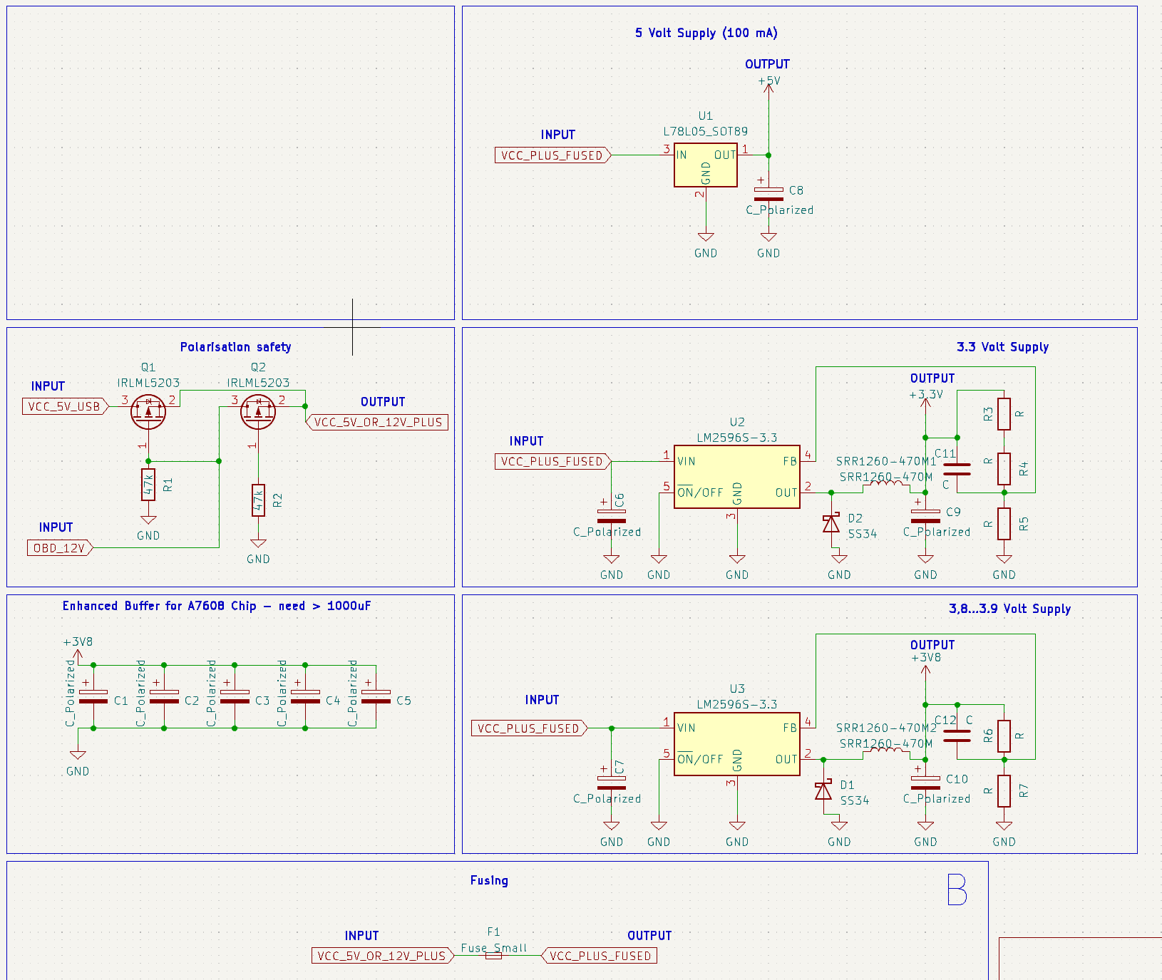
Schaltplan verschiedener Spannungsversorgungen
5 Volt Supply (100 mA) OUTPUT +5V U1 L78L05_5OT89 INPUT VCC_PLUS_FUSED IN OUT GND C8 C_Polarized GND Polarisation safety Q1 IRLML5203 Q2 IRLML5203 INPUT VCC_5V_DR_12V_PLUS OUTPUT GND R1 R2 OUTPUT 3.3 Volt Supply +3.3V U2 LM2596S-3.3 INPUT
in „Mosfet-P-Kanal“ · Analoge Elektronik und Schaltungstechnik · · Schaltpläne
-
 Bild
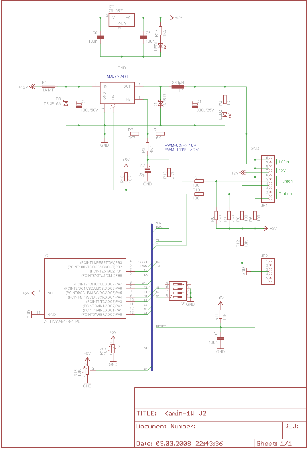
Schaltplan mit ATtiny24/44-84 Mikrocontroller und LM2575-ADJ Spannungsregler
IC2 78L05Z, VI, VO, +5V, GND, C5 100n, C6 100n, LED1 R17 10n, LM2575-ADJ, F1 1A MT, D3 P6KE15A, IN, OUT, 330uH L1, FB, D1 1N4937, C1 330u/25V, R4, R2 2K7, R1 4K7, PWM=0% => 10V, PWM=100% => 2V, GND, +5V, C3
in „DC/DC LM317 richtig einbauen“ · Analoge Elektronik und Schaltungstechnik · · Schaltpläne
-
PDF
ADNS-2700.pdf
only 0x2b 0x01 REV_ID Device Read only 0x01 0x02 MOUSE_STAT Device Read only Undefined 0x03 DELTA_X_L Device Read only 0x00 0x04 DELTA_Y_L Device Read only 0x00 0x05 DELTA_XY_H Device Read only 0x00 0x06 DZ Device Read only 0x00 0x07 SQUAL Device Read only 0x00 0x08 SHUT_HI Device Read only 0x00 0x09
in „USB Maus mit USART auslesen“ · Mikrocontroller und Digitale Elektronik ·
-
PDF
voltcraft_lsp1403_Maplin_N27GG_Manson_SSP-7080_Extech_382260_psu-adjustable-voltage-0-36-v-dc-0-5-a-80-w_sch.pdf
1 2 3 4 5 6 7 8 L1 NTC1 IN-N 120UH JNR13S2R5M CY1 1 L0 S1 CY6 L11 R1 CY3 DB1 2200PF 2200PF KBL407G R0 CX4 4700pF M1 680K/1W L3 4 2 GND 0.6mH 0.22uF CY7 CX1 20mH CX2 L4 HV SW DPST 20mH JVR-10N471K CY2 0.22UF 0.22UF 7mH
in „Voltcraft LSP-1403 Netztgerät zerschossen“ · Mikrocontroller und Digitale Elektronik ·
-
PDF
soft_clip.sch.pdf
100n 1k 47k P GND l GND GND GND GND GND U2 a C11 AT90S2313 22p i c 5 XTAL1 PB0(AIN0) 12 PB1nAIN1) 13 VCC B C12 X1 PB2 14 B 22p 10MHz PB3(OC1) 15 JP1 4 XTAL2 a PB4 16 1 PB5(MOSI) 17 2 1 RESET PB6(MISO) 18 3 GND c PB7(SCK) 19 4 VIN VCC 5 D3 U4 VeC PD0(RXD) 2 6 BAT43 78L05 PD1(TXD) 3 IN OUT 20 VCC PD2(INT0) 6 CLIP_DIG ISP CON2 GND M PD3(INT1) 7 CALL GND C14 PD4(T0) 8 C17 C15 C16 C18 - 100n PD5(T1) 9 +15...+20V 100u/25V 100n 100n 100u/16V VCC 10 GND PD6(ICP) 11 o r 2
in „CLIP Schaltplan; Protel->PDF Umwandlung bitte“ · Mikrocontroller und Digitale Elektronik ·
-
PDF
Bsp._1.pdf
D2 1N4148 IC3 +12V +5V IN OUT N G 78L05 C3 C2 R2 5 100NF 100NF C Binärausgang - N 10K 4 F 4 l 1 C1 1 N e W + D 1 R J 10µF IC1 PB0 VCC R1 T1 C4 PB1 PA0 C5 PB2 PA1 10K BC847 + PB3 PA2 IC2 100NF PB4 PA3 RS 485 VCC A PB5 PA4 1000µF B PB6 PA5
in „µC mit RS485 Treiber“ · Mikrocontroller und Digitale Elektronik ·
-
PDF
Bsp._2.pdf
D2 1N4148 IC3 +12V +5V IN OUT N G 78L05 C3 C2 R2 5 100NF 100NF C Binärausgang - N 10K 4 F 4 l 1 C1 1 N e W + D 1 R J 10µF IC1 PB0 VCC R1 T1 C4 PB1 PA0 C5 PB2 PA1 10K BC847 + PB3 PA2 IC2 100NF PB4 PA3 RS 485 VCC A PB5 PA4 1000µF B PB6 PA5
in „µC mit RS485 Treiber“ · Mikrocontroller und Digitale Elektronik ·
-
PDF
dogm204.pdf
d t t . t g l l l al l a ac r r / / / l r d t n e m i n i h ü e n l g g g g g t et w w t atatata t t t t a W C s s e T l h s S c r F V R R R R R I n nI P P D D D D D D D D E L L R= e s W . b c n e e f e L L L L L L L L L L L L a r n e n fl g d g n e - - - - - - H H/ H L H H H H H H H H / H H H L p f t n e e u e n e L s is t l ö s b t b z e o T T e D n w k r O c k a a m O V V V V V4 M M DD S D D D D D D D D E /
in „Probleme mit EADOGM204-4 und ATMEGA32“ · Mikrocontroller und Digitale Elektronik ·
-
PDF
MSV30245_Schematic_RevB.pdf
_5 P106/AN6/KI6 P03/D3 35 36 P10_4 KI6 P10_7 87 P107/AN7/KI7 P04/D4 82 D4 A18 37 37 38 38 VCC VCC P05/D5 81 D5 A19 39 39 40 40 P10_3 S4 Normal Mode/ S6B P06/D6 80 D6 CS0 41 41 42 42 P10_2 JP2 1 2 Attach Mode 4 P07/D7 79 D7 CS1 43 43 44 44 P10_1 5 P10/D8 78 D8 CS2 45 45 46 46 P10_0 R22 KI7 3 2 77 D9 CS3
in „m16C on Chip Programmierung“ · Mikrocontroller und Digitale Elektronik ·
-
PDF
625945.pdf
Characteristics 2 Characteristics Symbol Max Unit Thermal resistance, channel to case Rth (ch-c) 2.78 °C/W Thermal resistance, channel to ambient Rth (ch-a) 62.5 °C/W 1 Note 1: Ensure that the channel temperature does not exceed 150℃. Note 2: V DD = 90 V, Tch= 25°C(initial), L = 6.36 mAR I= 10 A, G =
in „Bauteilbestimmung H32 U3J“ · Mikrocontroller und Digitale Elektronik ·
-
PDF
SED1181.pdf
level output voltage V OL IOL = 0.6 mA — — V SS+0.4 V Input leakage current ILI 0 V ≤ VI≤ VSS — 0.05 2.0 A Output leakage current LO 0 V ≤ VO ≤ VSS — 0.05 5.0 A Shift clock XSCL — — 6.0 MHz Frame signal FR — 1/60 — sec Input capacitance C I T a= 25°C — 5.0 8.0 pF V SSH = –14.0 V Segment output on RSEG
in „Implementation eines komplexen SPI-Slaves“ · Mikrocontroller und Digitale Elektronik ·
-
PDF
vitrohm-crf-wirewound-safety-resistor-datasheet.pdf
10 K ] 120 ±50 Working Temperature Range [ºC] -55 … +350 Thermal Resistance [KW ]1 280 155 122 104 78 62 Max. Working Voltage [V]RMS Dielectric Withstanding Voltage [V]RMS 500 IEC115-1 clause 4.7 (1[min]) 4 1 Type Historical P/N: L max. Ø D max. * Ø d ±0,05 2 CRF251-4 / -8 n CRF110 9,0 3,0 0,65 i CRF200
in „Neff Steuerplatine Leiterbahnen abgerissen.“ · Platinen ·
-
PDF
Wohnraumuhr1_Rev1.1.pdf
p A A p A A p A A p A A +5V 1 C T D d D2 C C dD3 C C DA d D4 C C d D5 C C F V D G 1 2 E0 2 2 D 3 - L 2 - - A e A e 2 2A e 2 e 2 A +5V C T D S A E0 A A V O N S L 2 S , S G a b c d e f g , 6 a b c d e fg a b c d e f g 4 b c d e f g + GND 7 6 4 2 1 9 0 4 D7 6 4 2 1 9 0 D10 7 6 4 2 1 9 0 9 P 6 4 2 1 9 0
in „wohnraumuhr 2 - leiterplatte nach projekt scott huehn“ · Mikrocontroller und Digitale Elektronik ·
-
PDF
ssd1623.pdf
a i i n o a gh w r e v t r a v h e t e h h S r e v t l n t 3 l d l m l d l m l n l 3 d ag - i g n i g n d g - e - e t - e t e V0 Tsense Temperature sensor Data Compare and Output Control Waveform LUT V1 Voltage VDD sensor Data RAM 96 x 1 bits Data RAM 96
in „E-Ink Display im Blutzuckermeßgerät“ · Mikrocontroller und Digitale Elektronik ·
-
PDF
BAS70_1PS7XSB70_SER.pdf
1PS79SB70 SOD523 SC-79 single diode BAS70 SOT23 - single diode BAS70H SOD123F - single diode BAS70L SOD882 - single diode BAS70W SOT323 SC-70 single diode BAS70-04 SOT23 - dual series BAS70-04W SOT323 SC-70 dual series BAS70-05 SOT23 - dual common cathode BAS70-05W SOT323 SC-70 dual common cathode
in „[S] BAT54C Schottky“ · Markt ·
-
PDF
Verona_FS2052.pdf
+3V3 DC-DC PART DISPLAY PART +3V3 UT5504 Q5 10 R78 R84 68 P P L1 D S 4 . 0 6 220UH 10K R24 0 n 6 1 4 G R4 IC2 BACKLIGHT_CTRL 5 K C 1 C59 2 1 0 1 7 47U/16 D S 560 R1 SCA106 C 0 2 CN6 6 1 180 VCC_9V F 7 1 C 3 C C 1 Switch Drive8 R17 0.2 p R Q C C CollectorCollector
in „DAB-Modul - IR-FB-Anschluss-Pin? WELCHER PIN?“ · Mikrocontroller und Digitale Elektronik ·
-
PDF
AT89S8253-24PU.pdf
bytes are shifted in/out. Then the next instruction will be ready to be decoded. 39 3286I–MICRO–10/05 25. Flash and EEPROM Parallel Programming Modes ALE Address Data I/O P2.5:0, Mode RST PSEN EA P3.3 P3.4 P3.5 P3.6 P3.7 P0.7:0 P1.7:0 Serial Prog. Modes) H h h Chip Erase(2) H L 1.0 µs 12V H L H L L X
in „AT89S8253-24PU ersetzen“ · Mikrocontroller und Digitale Elektronik ·
-
PDF
NCP300L.PDF
) Vin(min) − 0.55 0.70 V (TA = −40°C to 85°C) − 0.65 0.80 Reset Output Current (Pin 1, Active Low ‘L’ Suffix Devices) OUT mA N−Channel Sink Current, NCP300, NCP301 0.01 0.05 − (VOUT = 0.05 V, in= 0.70 V) (VOUT = 0.50 V, in= 0.85 V) 0.05 0.50 − P−Channel Source Current, NCP300 (VOUT = 2.4 V, in= 4.5
in „High-Side-Strom auf Low-Side spiegeln (Stromspiegel?!)“ · Analoge Elektronik und Schaltungstechnik ·
-
PDF
Technical-Information-Interfacing-with-VE-Bus-products-MK2-Protocol-3-14.pdf
24-bit values. <Phase info> indicates which phase the received frame describes, and in the case of L1, how many phases are present in the system. <Phase info> Meaning 0x05 This frame describes L4. 0x06 This frame describes L3. 0x07 This frame describes L2. 0x08 This frame describes L1; there is 1 phase
-
PDF
LTC1174.pdf
100 3 1 8 125 LB IN VOUT 3.3 F** VOUT 10 145 2 LTC1174HV-5 5 5V 12 160 LB OUT SW † 135mA AT 13 180 L1A V = 9V GND † 100 H IN 4 L1B 3 2 MBRS140T3 100 H MBRS140T3 + 100 F* CTX100-4 L1A 16V L1B 4 1 + 100 F* –VOUT 16V –5V 1174 T135mA AT V = 9V IN 9V to 12V, –12V Outputs INPUT VOLTAGE 4V TO 12.5V * AVX TAJD226K035
in „DC/DC Wandler LTC1174 Verhalten bei Shutdown?“ · Mikrocontroller und Digitale Elektronik ·
-
PDF
MEGA48V_88V_168V.pdf
and ICR1 Registers. Note that when using “C”, the compiler handles the 16-bit access. 110 2545T–AVR–05/11 ATmega48/88/168 Assembly code examples(1) ... ; Set TCNT1 to 0x01FF ldir17,0x01 ldir16,0xFF outTCNT1H,r17 outTCNT1L,r16 ; Read TCNT1 into r17:r16 in r16,TCNT1L in r17,TCNT1H ... (1) C code examples
in „analog comparator interrupt probleme mit atmegas“ · Mikrocontroller und Digitale Elektronik ·
-
PDF
Fensterkomparator_Hysterese.pdf
1 2 3 4 5 6 4 P + T IN OUT 8 GND A Stromversorgung IC1P C1 IC3 C2 A 100n 78L05 100n O 1 4 P1 P P S TSchaltausgang T GND 8 T 5 + 4 + k 6 k 8 1 R 1 R B 4 B 220k 4 V D 1 14052 + TP5 R2 2 E E TError 0 S 10k 3 IC1A L R 2 R1k R1 1 A 2 LM393N 74HC00N IC2C 1 IC2A 5 6 9 8 R9 GND 3 4
in „Ausgang schalten bei Eingang zwischen zwei Spannungswerten“ · Analoge Elektronik und Schaltungstechnik ·
-
PDF
10134fd.pdf
V S= ±2V to ±18V l 100 117 100 117 97 116 dB Ratio VOUT Output Voltage Swing R L 2k l ±12 ±13.8 ±12 ±13.8 ±11.5 ±13.8 V V S 5V, 0V R L 600Ωto Ground Output Low l 6 15 6 15 6 18 mV Output High l 3.2 3.8 3.2 3.8 3.1 3.8
in „LT1013 Unterschied D und P Package“ · Analoge Elektronik und Schaltungstechnik ·
-
PDF
Frequenznutzungsplan2011pdf.pdf
Kanalraster: 20 kHz Frequenznutzungsteilplan: 182 Eintrag: 182008 Stand: AUGUST 2011 Frequenzbereich: 75,2 - 78,7 MHz Nutzungsbestimmung(en): 5 31 Funkdienst: MOBILER LANDFUNKDIENST Nutzung: ziv Frequenznutzung: Funkanwendungen öffentlicher Eisenbahnen Frequenzteilbereich(e): 78,42 - 78,7 MHz Frequenznutzungs-
in „Interessante Frequenzen zwischen 100KHz und 2GHz“ · HF, Funk und Felder ·
-
Datei
lab9a_c180.txt
$20 $0D LD9EA ldab L1000 ;$D9EA $F6 $10 $00 cmpb #'z' ;$D9ED $C1 $7A bne LD9EA ;$D9EF $26 $F9 com L0001 ;$D9F1 $71 $00 $01 clr L1000 ;$D9F4 $79 $10 $00 LD9F7 bra LD9EA ;$D9F7 $20 $F1 inc L1000 ;$D9F9 $72 $10 $00 ldab #$80
in „HCS12 CPU Disassembler“ · Mikrocontroller und Digitale Elektronik ·
-
PDF
Hoa2498_1.pdf
thermoplastic housing. The .250(6.35) detector responds to radiation from the IRED only when .070(1.78) a reflective object passes within its field of view. The .625(15.88) HOA2498 series employs metal can packaged .450(11.43) .50(12.7) TEST components. For additional component information see .75(19.05
in „HOA2498_001 reflective sensor zu verschenken“ · Mikrocontroller und Digitale Elektronik ·
-
PDF
Hoa2498_1.pdf
thermoplastic housing. The .250(6.35) detector responds to radiation from the IRED only when .070(1.78) a reflective object passes within its field of view. The .625(15.88) HOA2498 series employs metal can packaged .450(11.43) .50(12.7) TEST components. For additional component information see .75(19.05
in „EEproms 24C32 zu verschenken“ · Mikrocontroller und Digitale Elektronik ·
-
PDF
A300_PCA9538_NXP.pdf
DD - 5.5 V IOL LOW-level output current VOL = 0.4 V 3 7 - mA I leakage current V = V = V −1 - +1 A L I DD SS C i input capacitance VI= V SS - 5 10 pF PCA9538_5 © NXP B.V. 2009. All rights reserved. Product data sheet Rev. 05 Ñ 28 May 2009 13 of 28 NXP Semiconductors PCA9538 2 8-bit I C-bus and SMBus
in „I²C-I/O-Expander mit TRI-state Output“ · Mikrocontroller und Digitale Elektronik ·
-
PDF
SI7611.pdf
TYPICAL CHARACTERISTICS 25 °C, unless otherwise noted 1 Duty Cycle = 0.5 t 0.2 e s a c 0.1 T a 0.1 e e 0.05 t p Notes: e l 0.02 E a P d r DM z h a T 0.01 t1 r 2 o 1. Duty Cycle, D = N t2 Single Pulse 2. Per Unit BasethJA 81 °C/W 3. JM- A = DM thJAt) 4. Surface Mounted 0.001 10-4 10 -3 10-2 10 -1 1 10 100 1000
in „gleichwertiger Ersatztyp für Mosfet gesucht“ · Analoge Elektronik und Schaltungstechnik ·
-
PDF
ads1220.pdf
90 18.88 (16.56) 18.80 (16.72) 18.91 (16.65) 175 18.27 (15.92) 18.32 (15.82) 18.36 (15.72) 330 17.78 (15.41) 17.94 (15.32) 17.73 (15.12) 600 17.31 (14.85) 17.29 (14.68) 17.32 (14.65) 1000 16.72 (13.94) 16.76 (14.05) 16.72 (13.97) Table 5. Noise in μV RMS (μV PP at AVDD = 3.3 V, AVSS = 0 V, Turbo Mode
in „ADS1220 Temperatur SPI“ · Mikrocontroller und Digitale Elektronik ·
-
PDF
AN1819.pdf
Bourns CRM2512-JW-5R1ELF R5 4.7 1206 SMT Yaego RC1206JR-074R7L R7, R9 10 2512 SMT Bourns CRM2512-JW-10R0ELF R8, R12 15 50W TO-220 Bourns PWR220-2FD15R0F R10, R11 10k 1206 SMT Yaego RC1206JR-0710KL R15 390 1206 SMT Yaego RC1206JR-07390RL R16 20 1206 SMT Yaego RC1206JR
in „Stackpole Ferrit Kerne für RF Verstärker“ · HF, Funk und Felder ·
-
PDF
MLX90640-Datasheet-Melexis.pdf
position as Pix(i,j) where i is its row number (from 1 to 24) and j is its column number (from 1 to 32) 2 l l l l C C C C Row 1 Row 2 Row 3 Row 24 VDD 0 GND SDA SCL Reference tab Figure 3 Pixel in the whole FOV REVISION 11 – 3 AUGUST 2018 Page 10 of 60 MLX90640 32x24 IR array Datasheet 10.2. Communication
in „MLX90640 IR-Array 32x24 pixel“ · Mikrocontroller und Digitale Elektronik ·
-
PDF
MLX90640-Datasheet-Melexis.pdf
position as Pix(i,j) where i is its row number (from 1 to 24) and j is its column number (from 1 to 32) 2 l l l l C C C C Row 1 Row 2 Row 3 Row 24 VDD 0 GND SDA SCL Reference tab Figure 3 Pixel in the whole FOV REVISION 11 – 3 AUGUST 2018 Page 10 of 60 MLX90640 32x24 IR array Datasheet 10.2. Communication
in „Wärmebildkamera mit dem MLX90640 und Arduino Due“ · Mikrocontroller und Digitale Elektronik ·
-
PDF
4088fb.pdf
PARAMETER CONDITIONS MIN TYP MAX UNITS Input Power Supply VBUS Input Supply Voltage l 4.35 5.5 V I Total Input Current 1x Mode l 92 97 100 mA BUS(LIM) 5x Mode l 445 470 500 mA 10x Mode l 815 877 1000 mA Low Power Suspend Mode l 0.32 0.39 0.50 mA High Power Suspend Mode l 1.6 2.05 2.5
in „[EAGLE Anfänger] Package finden oder herstellen“ · Platinen ·
-
PDF
sn74lv367a.pdf
SCLS398G − APRIL 1998 − REVISED APRIL 2005 FUNCTION TABLE (each buffer/driver) INPUTS OUTPUT OE A Y L H H L L L H X Z logic diagram (positive logic) 1OE 1 2OE 15 1A1 2 3 1Y1 2A1 12 11 2Y1 To Three Other Channels To One Other Channel Pin numbers shown are for the D, DB, DGV, J, NS, PW, and W packages.
in „Gesucht: "Inhibit" Gate“ · Mikrocontroller und Digitale Elektronik ·
-
PDF
condensator.pdf
x23,0 134 1860 1,79 KPQS/5,6/400 5,60 21,0x36,0 134 1350 3,43 Q4/2,2/400 2,20 16 x23,0 134 1861 2,05 KPQS/6,8/400 6,80 23,0x36,0 134 1360 3,78 Q4/2,7/400 2,70 18 x23,0 134 1862 2,30 KPQS/8,2/400 8,20 26,0x36,0 134 1370 4,70 Q4/3,3/400 3,30 16 x35,0 134 1863 2,30 KPQS/10/400 10,0 28,0x36,0 134 1380 5,27
in „Kennzeichnung Kondensator Q4“ · Analoge Elektronik und Schaltungstechnik ·
-
PDF
apem_08162017_16300-1158414.pdf
tra01 b own yellow 12 transparent green 0 03 03 gr yw 18 18 tra02 g ent red 14 transparent yellow 2 05 golden n 04 04 yellow 03 grey 18 transparent red s 05 05 golden 04 yellow a 3 06 06 whitee 05 golden e 0 Ordering example: 15501 + 16270 + 1630008 + 16325 9 + 1632708 + 1692208 3 m3. Ordering example
in „Suche Einbautaster mit 2 Leuchtanzeigen“ · Analoge Elektronik und Schaltungstechnik ·
-
PDF
PSMN8R7-80PS_MOSFET.pdf
symbol 1 G gate 2 D drain mb D 3 S source G mb D mounting base; connected to drain mbb076S 1 2 3 SOT78 (TO-220AB) 3. Ordering information Table 3. Ordering information Type number Package Name Description Version PSMN8R7-80PS TO-220AB plastic single-ended package; heatsink mounted; 1 mountinSOT78 hole
in „Motoransteuerung Pi und PWM“ · Mikrocontroller und Digitale Elektronik ·
-
PDF
Audiomodul.pdf
. 4 1 1 8 1 1 / I / / I / / / / / / 4 E S O L S L A M L L _ S O I C O C T 2 C C A K K D D D X _ _ R _ B D L _ S G L L G G G U R S D S _ S C R S F H H M A B _ U C _ A U _ / / A B D C B C I I D A _ D V n 3 0 1 2 3 A 6 0 K L L L L T 0 C 1 N H H H H
in „"Unwichtige" Fragen für die Schaltplan-Optik“ · Platinen ·