-
Bild
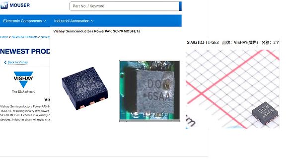
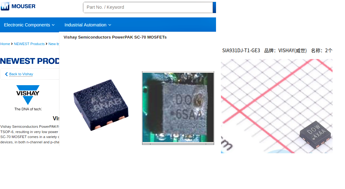
Screenshot einer Mouser-Webseite mit Vishay MOSFET-Produktbildern
Components Industrial Automation Home > NEWEST Products > New b Vishay Semiconductors PowerPAK SC-70 MOSFETs SIA931DJ-T1-GE3 品牌: VISHAY(威世) 名称: 2个 NEWEST PROD Back to Vishay VISHAY The DNA of tech. Vishay Semiconductors PowerPAK TSOP-6, resulting in very low power SC-70 MOSFET comes in a variety devices,
in „SMD Bauteil gesucht (Danalock Smartlock)“ · Analoge Elektronik und Schaltungstechnik · · Screenshots
-
PDF
MAX856-Stepup.pdf
GND Power Ground. Must be low impedance; solder directly to ground plane. 8 8 LX N-Channel Power-MOSFET Drain _______________Detailed Description The peak switch current of the internal MOSFET power switch is fixed at 500mA ±100mA (MAX856/MAX857) Operating Principle or 125mA ±25mA (MAX858/MAX859). The
in „Bitte mal kurz über Schaltplan drüberschauen“ · Mikrocontroller und Digitale Elektronik ·
-
PDF
MAX856-Stepup.pdf
GND Power Ground. Must be low impedance; solder directly to ground plane. 8 8 LX N-Channel Power-MOSFET Drain _______________Detailed Description The peak switch current of the internal MOSFET power switch is fixed at 500mA ±100mA (MAX856/MAX857) Operating Principle or 125mA ±25mA (MAX858/MAX859). The
in „Verständnisfrage zu Shutdown Feature von Schaltregler MAX856“ · Mikrocontroller und Digitale Elektronik ·
-
PDF
bd7690fj-e.pdf
diagram is shown in Figure 4. The switching operation is shown in Figure 5. Switching Operation 1. MOSFET is turned on, andLI increases 2. The IC compares VEOwith Vramp, and MOSFET is off when the Vramp voltage higher thanEO 3. MOSFET is off, andLI decreases 4. The IC detects a zero point ofLthe I in ZCD and turns on MOSFET IL Auxiliary winding for zero Diode current detection Bridge PFC OUT ACIN FRD MOSFET OUT ZCD PFC OUT VS Feedback Resistance EO CS GND RCS GND OCP detected Resistance Figure 4. Operation circuit outline
in „Modulierung eines Hochsetzstellers mit PFC-Steuerung in PLECS – Hilfe bei Grundlagen der Steuerung g“ · Analoge Elektronik und Schaltungstechnik ·
-
Bild
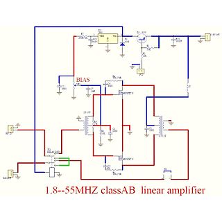
Schaltplan eines 1,8--55MHz Class-AB Linearverstärkers
C3 100UF GND Vin Q1 SS50 12V-16V C2 100UF R1 50R R2 10K BIAS VR1 C4 100N R6 200-270R PIT C7 10N MOSFET N RF-IN TQ1 RELAY-DPDT C6 27R R3 10K C3 100N C1 100N TQ2 MOSFET N C5 100N R5 200-270R RF-OUT 1.8--55MHZ classAB linear amplifier
in „MiniPA100 Schema“ · HF, Funk und Felder · · Schaltpläne
-
Bild
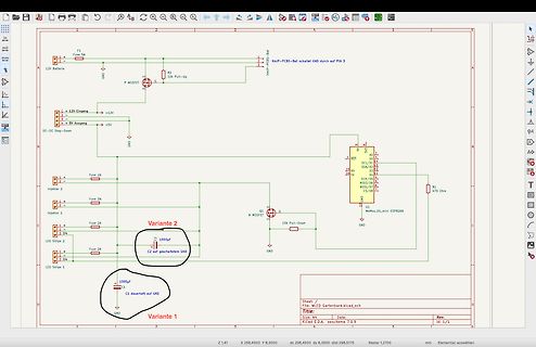
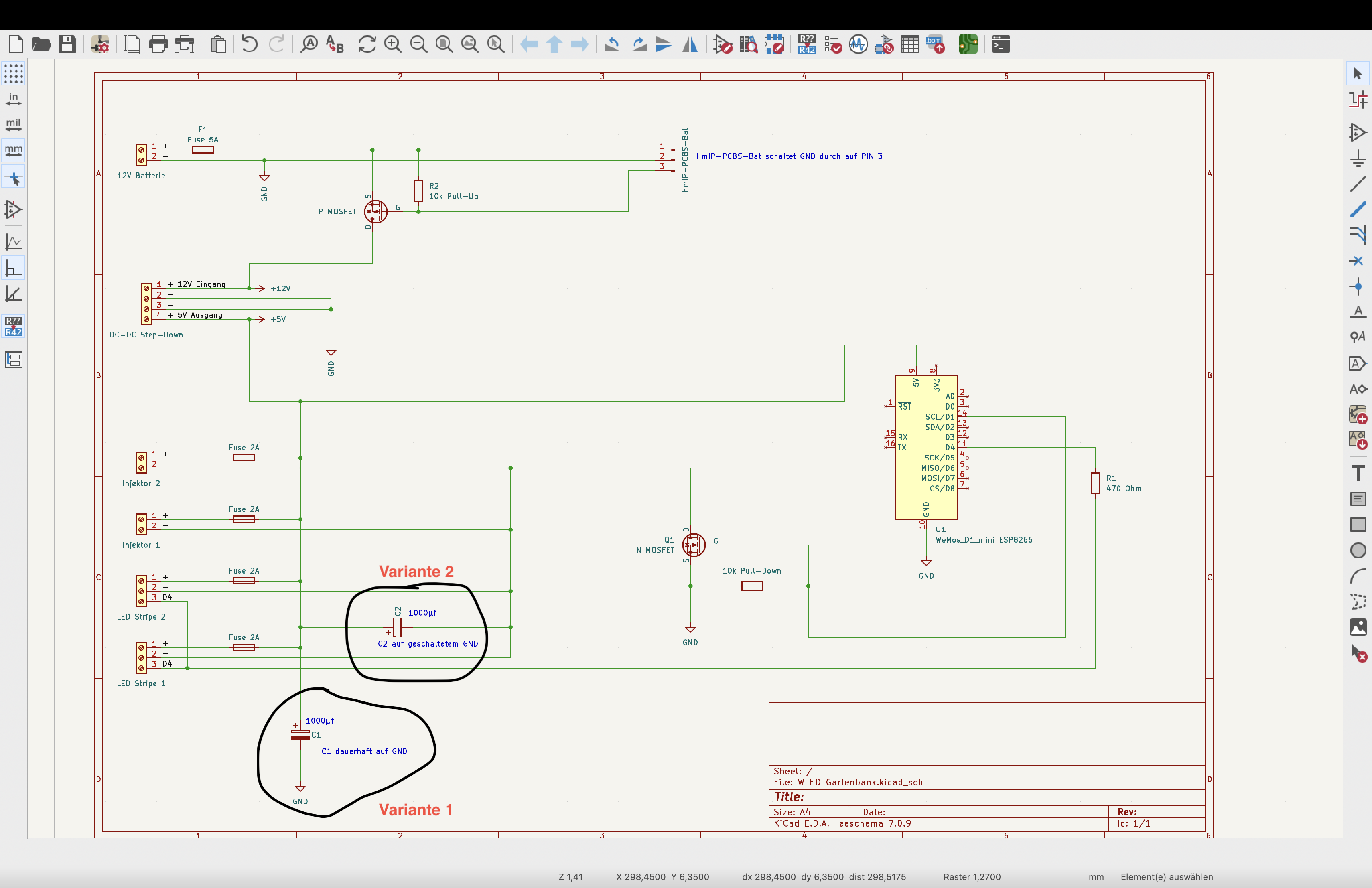
Schaltplan in KiCad mit ESP8266 und LED-Treiber
F1 Fuse 5A, 12V Batterie, GND, P MOSFET, R2 10k Pull-Up, 12V Eingang, +12V, DC-DC Step-Down, +5V, GND, Fuse 2A, Injektor 2, Fuse 2A, Injektor 1, Fuse 2A, LED Stripe 2, C2 1000uf, Variante 2, C2 auf geschaltet GND, LED Stripe 1, C1 1000uf, Variante 1, C1 dauerhaft auf GND, GND, Wemos_D1_mini ESP8266, P1 470 Ohm, Q1 N MOSFET, 10k Pull-Down, GND, Sheet: WLED Gartenbank.kicad_sch, Title:, Size: A4, Date:, Rev:, Id: 1/1
in „Einbauposition Kondensator“ · Analoge Elektronik und Schaltungstechnik · · Screenshots
-
Bild
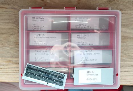
Sortierbox mit elektronischen Bauteilen und Beschriftungen
B5819WS Schottky Diode 30V 0,4V bei 0,1A 0,8V bei 1A IRLML6433 N-MOSFET max 30V 4A 37 mOhm bei VGS 2,5V TLV431A Adjustable Shunt Regulator ref 1,25V max 6V 15mA IRLML6402 P-MOSFET max 20V 3A 135 mOhm bei VGS 2,5V 74LVC1G17 1x Schmitt Trigger Buffer 1,6 - 5,5V 24 mA bei
in „Quick&dirty - schnelle Problemlösungen selbst gebaut“ · Projekte & Code · · Fotos
-
PDF
mppt_emv_analyse.pdf
Probleme: 1. Große freie Fläche oben links wirkt als Antenne (ist aber notwendig zur Kühlung des HS MOSFET) 2. Abgriff für interne 10V Spannungsversorgung (unten) wirkt als Antenne Hinweis: GND Verbindung liegt direkt darunter, siehe nächste Folie Bottom layer, GND markiert Mögliche Probleme: 3. Verbindung
in „EMV-Test DC/DC - Verbesserungsvorschläge gesucht“ · Analoge Elektronik und Schaltungstechnik ·
-
Bild
ISOCOM Photocoupler CHD320E Produktpräsentation
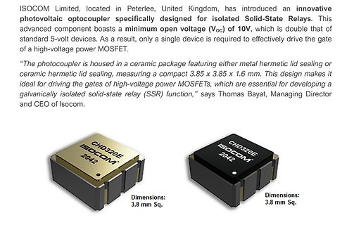
a result, only a single device is required to effectively drive the gate of a high-voltage power MOSFET. "The photocoupler is housed in a ceramic package featuring either metal hermetic lid sealing or ceramic hermetic lid sealing, measuring a compact 3.85 x 3.85 x 1.6 mm. This design makes it ideal for driving the gates of high-voltage power MOSFETs, which are essential for developing a galvanically isolated solid-state relay (SSR) function," says Thomas Bayat, Managing Director and CEO of Isocom. CHD320E ISOCOM 2042 Dimensions: 3.8 mm Sq.
in „AI-VNA, 6GHz-Oszilloskop von Rigol, NEC-Frontend uvam“ · Mikrocontroller und Digitale Elektronik · · Screenshots
-
PDF
STS7C4F30_STripFET.pdf
STS7C4F30L N-CHANNEL 30V - 0.018 - 7A SO-8 P-CHANNEL 30V - 0.070 - 4A SO-8 STripFET™ POWER MOSFET TYPE V DSS RDS(on) D STS7C4F30L(N-Channel) 30 V <0.022 7 A STS7C4F30L(P-Channel) 30 V <0.080 4 A ■ TYPICAL R DS(on) (N-Channel) = 0.018 ■ TYPICAL R DS(on) (P-Channel) = 0.070 ■ STANDARD OUTLINE FOR EASY AUTOMATED SURFACE MOUNT ASSEMBLY ■ LOW THRESHOLD DRIVE DESCRIPTION SO-8 This Power MOSFET is the latest development of STMicroelectronis unique "Single Feature Size™" strip-based process. The resulting transistor shows extremely high packing density for low on- resistance, rugged avalanche
in „[S] STS7C4F30L StripFET“ · Markt ·
-
Bild
Schaltplan einer Hochspannungsstufe mit Villard-Kaskade
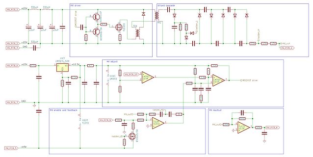
HV_PCB_1 +15V 330uH 330uH HV driver BC547B 470 22uF 22uF 22uF 2MOSFET drive FL1100 TR1 TR2 Villard cascade LD_ladder_H 33k 15k HV_out HV_PCB_4 HV_PCB_2 330uH HV_PCB_3 GND HV adjust LM317L_508 V+ 47 11.5V U14C LM393 U14A 2.2k 47 10k 5.1k 5.1k 22k 6 LM393 U14B MOSfet drive
in „Pollin PMT-Modul“ · Mikrocontroller und Digitale Elektronik · · Schaltpläne
-
Bild
Forenbeitrag über ESP32 und MOSFET-Berechnung
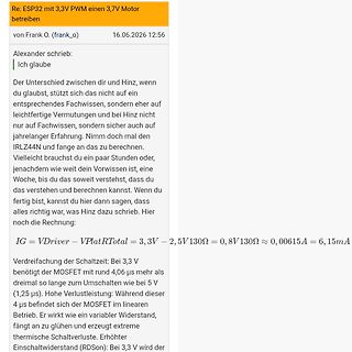
VPlatRTotal = 3,3V - 2,5V 130Ω = 0,8V 130Ω ≈ 0,00615A = 6,15mA Dreidreifung: Bei 3,3 V benötigt der MOSFET mit rund 4,06 µs mehr als dreimal so lange zum Umschalten wie bei 5 V (1,25 µs). Hohe Verlustleistung: Während dieser 4 µs befindet sich der MOSFET im linearen Betrieb. Er wirkt wie ein variabler Widerstand
in „ESP32 mit 3,3V PWM einen 3,7V Motor betreiben“ · Analoge Elektronik und Schaltungstechnik · · Screenshots
-
PDF
en.DM00023581.pdf
clamp protect the chip in harsh MOSFET (analog driving) environments. ■ Compatible with standard Power MOSFET Fault feedback can be detected by monitoring voltage at the input pin Table 1. Device summary Order codes Package Tube Tape and
in „Trix Mobile Station seltsamer Fehler“ · Mikrocontroller und Digitale Elektronik ·
-
Datei
bss89.txt
*SRC=BSS-89;BSS-89;MOSFETs N;Siemens;240V 290mA 6 Ohm *SYM=N-MOSFET .SUBCKT BSS-89 1 2 3 LS 5 2 7N LD 95 3 5N RG 4 11 5.5M RS 5 76 164M DSS89 76 95 DREV .MODEL DREV D CJO=0.04N RS=20M TT=30N IS=300P BV=240 MSS89 86 11 76 76
in „Wandler Kühlschrank: Rätselhafter Schaltplan.“ · Analoge Elektronik und Schaltungstechnik ·
-
Datei
bss92.txt
*SRC=BSS-92;BSS-92;MOSFETs P;Siemens;240V 150mA 20 Ohm *SYM=P-MOSFET .SUBCKT BSS-92 1 2 3 LS 5 2 7N LD 97 3 5N RG 86 87 5.5M RS 5 76 886M D92 97 76 DREV .MODEL DREV D CJO=0.05N RS=20M TT=35N IS=300P BV=240 M92 98 87 76 76 MBUZ
in „Wandler Kühlschrank: Rätselhafter Schaltplan.“ · Analoge Elektronik und Schaltungstechnik ·
-
Datei
Liontron_LTDUC_RS485.txt
F40C Zelle 1 Spannung (mv) F70C Zelle 2 Spannung F20C Zelle 3 Spannung F10C Zelle 4 Spannung 4102 Mosfet Temp 3D02 Zelltemp 9B250F46 SOC 00384F46 Gesamtspannung 18C20546 Strom in ma BC7CB93D Enladene Leistung Zyklus 00000000 Geladene Leistung Zyklus 1C00 Anzahl Ladezyklen 00000000000000000000 Reserviert
in „Amateure braucht Hilfe bei RS232“ · Mikrocontroller und Digitale Elektronik ·
-
Bild
Screenshot eines Datei-Upload-Fensters und einer Excel-Tabelle
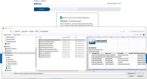
Operationsverstärker 5 942-IRF7I30TPBF IRF7I30TPBF Infineon Diodes Incorporated 6 621-DMT302LS3D DMT302LS3D MOSFET MOSFET
in „[S] Sammelbestellung Mouser“ · Markt · · Screenshots
-
PDF
Infineon-AN2017-10_Eval-M1-05F804-AN-v01_00-EN.pdf
Symbol Description Min Max Unit VDS MOSFETDrain-to-Source Voltage --- 40 V IO MaximumDC currentperMOSFET@TC=25°C --- 80 A (Note1) Pd MaximumPowerdissipationperMOSFET@TC --- 13 W =100°C TJ(MOSFET& MaximumOperatingJunctionTemperature --- 150 °C IC) TS Storage Temperature Range -40 150 °C VGS GatetoSource
in „Brushlessmotor mit Infineon Power Board betreiben“ · Mikrocontroller und Digitale Elektronik ·
-
PDF
sevconSBPM.pdf
state 9 22 Autozero Fault The current measurement autozero value is not 10 in the permitted range. MOSFETs Short The armature MOSFETs have been detected as 23 Circuit being short circuit. 3 MOSFETs did not pulse during power on 24 MOSFET Off failsafe checks (failsafe circuit enabled). 0 25 MOSFET On MOSFETs pulsed during power on failsafe 0 checks (failsafe circuit disabled). Power Up MOSFET The armature MOSFETs have been detected as 26 Short Circuit being short circuit at system power up. 3 Contactor 2 did not pulse during power on 27 Drive 2 Off failsafe checks (failsafe circuit enabled
in „Sevcon Millipak Steuerung Batteriespannung ändern“ · Mikrocontroller und Digitale Elektronik ·
-
PDF
irf7389.pdf
PD - 91645A IRF7389 ® HEXFET Power MOSFET l Generation V Technology N-CHANNEL MOSFET N-Ch P-Ch l Ultra Low On-Resistance S1 1 8 D1 l Complimentary Half Bridge G1 2 7 D1 l SurfaceMount V DSS 30V -30V S2 3 6 D2 l FullyAvalancheRated G2 4 5 D2 P-CHANNEL MOSFET R 0.029Ω 0.058Ω DS(on) Description Top View FifthGenerationHEXFETsfromInternationalRectifier utilize advanced processing techniques to achieve extremely low on-resistance per silicon area. This benefit
in „Treiber für Push-Pull 12V?“ · Mikrocontroller und Digitale Elektronik ·
-
PDF
irf7389.pdf
PD - 91645A IRF7389 ® HEXFET Power MOSFET l Generation V Technology N-CHANNEL MOSFET N-Ch P-Ch l Ultra Low On-Resistance S1 1 8 D1 l Complimentary Half Bridge G1 2 7 D1 l SurfaceMount V DSS 30V -30V S2 3 6 D2 l FullyAvalancheRated G2 4 5 D2 P-CHANNEL MOSFET R 0.029Ω 0.058Ω DS(on) Description Top View FifthGenerationHEXFETsfromInternationalRectifier utilize advanced processing techniques to achieve extremely low on-resistance per silicon area. This benefit
in „Brushless DC Motorsteureung Dysfunktion AVR444“ · Analoge Elektronik und Schaltungstechnik ·
-
PDF
IRLU2905.pdf
PD - 95774B IRLR2905ZPbF IRLU2905ZPbF Features HEXFET Power MOSFET l Logic Level D l Advanced Process Technology V DSS = 55V l Ultra Low On-Resistance l 175°C Operating Temperature R = 13.5mΩ l Fast Switching G DS(on) l Repetitive Avalanche Allowed up to Tjmax l Lead-Free D = 42A S Description This HEXFET Power MOSFET utilizes the latest processingtechniquestoachieveextremelylowon- resistance per silicon area. Additional features of this design are a 175°C junction operating temperature, fast switching speed and
in „Batterieschutzschaltung. Murks oder möglich?“ · Analoge Elektronik und Schaltungstechnik ·
-
PDF
12__flyback_snubber_design.pdf
not solved the EMI problem of the ringing waveform. age is given by: Figure 4c: Flyback converter MOSFET voltage with primary RCD clamp and decreased dissipa- tion (ie increased and the power dissipation is given by: value for vx) The ringing can subsequently be damped out again by reintroducing the RC
in „Erzeugt ein 9V-Printtrafo mehr als 750V?“ · Analoge Elektronik und Schaltungstechnik ·
-
PDF
irf740pbf.pdf
IRF740, SiHF740 Vishay Siliconix Power MOSFET FEATURES PRODUCT SUMMARY • Dynamic dV/dt Rating VDS (V) 400 Available R (Ω) V = 10 V 0.55 • Repetitive Avalanche Rated DS(on) GS RoHS* Qg(Max.) (nC) 63 • Fast Switching COMPLIANT • Ease of Paralleling
in „Bauteilbestimmung H32 U3J“ · Mikrocontroller und Digitale Elektronik ·
-
PDF
TP4067.pdf
TP4067 因热反馈的缘故而减小充 STDBY=强下拉 电电流的条件可通过 IC 中的功率损耗 图 4 一个典型充电循环的状态图 来估算。 这种功率损耗几乎全部都是由 稳定性与可靠性的考虑 内部 MOSFET 产生的――这可由下式 在没有接电池时,为了防止接入 近似求出: VCC 或 BAT 产生高能毛刺,强烈要求 PD (VCCVBAT)BAT VCC和 BAT 端各加一个 10μF 电容器。 式中的 P 为D散的功率, VCC为输 在恒定电流模式中,位于反馈环路 入电源电压,V BAT为电池电压,I BAT 中的是 PROG 引脚,而不是电池。恒 为充电电流。当热反馈开始对 IC 提供
in „LiFePo4 3,2V Ladegerät“ · Analoge Elektronik und Schaltungstechnik ·
-
PDF
WD3133-WillSEMI.pdf
WD3133 is a high efficiency, high power, peak current mode step-up converter. Internal 0.35Ω HV power MOSFET with Min. 1A current limit. For portable device with Li-ion battery application, WD3133 could output typical 12V / 200mA ~300mA from 3.3V~5V input. SOT-23-5L The boost converter WD3133 runs in Pulse-Width
in „Vergleichstyp WD3133“ · Analoge Elektronik und Schaltungstechnik ·
-
Bild
Datenblatt des BP9022A LED-Treibers
input. The output power of system is recommended to less than 5W. The BP9022A integrates 650V power MOSFET. Since adopting primary sense and feedback control technology, the secondary sense and feedback circuit is eliminated. The loop compensation components are also removed while maintaining stability
in „Metabo 0334440900 LED Netzteil“ · Haus & Smart Home · · Screenshots
-
PDF
bq2057w.pdf
REVISED JULY 2002 APPLICATION INFORMATION selecting an external pass-transistor (continued) P-channel MOSFET: Selection steps for a P-channel MOSFET: Example: V = 5.5 V, I = 500 mA, 4.2-V single-cell Li−Ion I (REG) (bq2057C). V Is the input voltage to the charger an(REG) is the desired charge current. (See
in „LiPo Lader BQ2057 schaltet nicht ab“ · Mikrocontroller und Digitale Elektronik ·
-
PDF
SSL21084.pdf
stored in inductor L each period that the switch is on. The inductor current ILis zero when the MOSFET is switched on. The amplitude of the current build-up in L is proportional to the voltage drop over the inductor and the time that the MOSFET switch is on. When the MOSFET is switched off, the energy
in „LED Leuchte 230V - Nur jede 2te LED defekt?“ · Analoge Elektronik und Schaltungstechnik ·
-
PDF
FL5150-D.pdf
for controlling the pulse width for external IGBT User Programmable Leading or Trailing Edge or MOSFET transistors. The pulse width can be user P Dimming Control programmable with either an external resistor or 0 to 10 V Dynamic Over-Current and Temperature Protection DC signal or controlled by a
-
PDF
ab-EVAL6229PD.pdf
62▯▯ L6229 features a non-dissipative overcurrent ▯▯▯▯▯▯▯▯▯▯▯▯ protection on the high-side Power MOSFETs and thermal shutdown. Table 1. Order codes Features Part number Package Operating supply voltage from 8 to 52 V L6229N PowerDIP24 2.8 A output peak current (1.4 A DC) R DS(ON) 0.73 typ. value
in „BLDC Motor rotiert nicht trotz Spannung“ · Analoge Elektronik und Schaltungstechnik ·
-
Bild
Schaltplan eines Gate-Treiber-ICs mit MOSFET-Ausgang
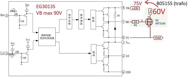
EG3013S VB max 90V HIN 15K 15K Vcc 电平移 脉冲滤波 驱动 死区时间电路 闭锁电路 8 VB +15V 75V B0515S (trafo) 60V V+ 10 R6 2 IRF3206 Q2 6 VS Out2 1 Vc 5 LO 4 GND
in „Wie 20-40A high side (n-Ch 2,4 mOhm) bei 20-60V und 2 kHz 50% duty pwm ?“ · Analoge Elektronik und Schaltungstechnik · · Schaltpläne
-
Bild
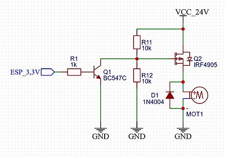
Schaltplan einer Transistor-Mosfet-Treiberstufe für einen Motor
VCC_24V, R11, 10k, Q2, IRF4905, R12, 10k, D1, 1N4004, MOT1, GND, Q1, BC547C, R1, 1k, ESP_3,3V
in „IRF4905 Ansteuerung mittels ESP32 (24V 2A)“ · Mikrocontroller und Digitale Elektronik · · Schaltpläne
-
Bild
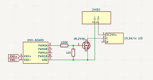
Schaltplan einer LED-Ansteuerung mit KNX-Board und MOSFET
24VDC, V-, V+, 1, 2, DC24V+, 2, 3, C, W, 19,2W/m LED, IRLZ44N, 1, 2, 3, 100R, 10k, KNX-BOARD, PWM0A, 3, PWM0B, 4, PWM1A, 5, PWM1B, 6, 7, GND, KNX+, 1, KNX-, 2
in „KNX Controller - LED driver galvanisch trennen“ · Mikrocontroller und Digitale Elektronik · · Schaltpläne
-
Bild
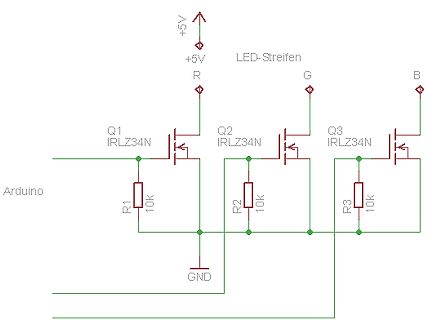
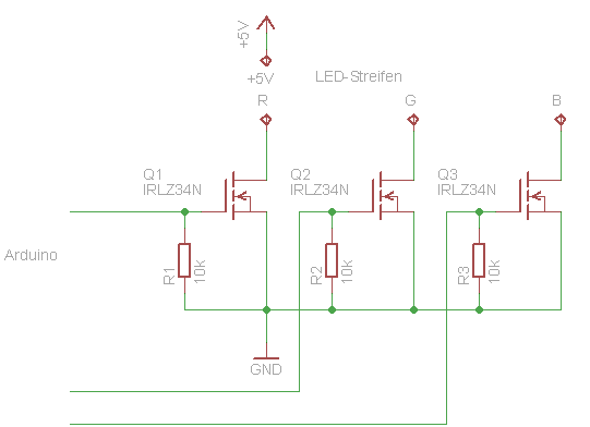
Schaltplan zur Ansteuerung eines RGB-LED-Streifens mit MOSFETs
+5V LED-Streifen R G B Q1 IRLZ34N Q2 IRLZ34N Q3 IRLZ34N R1 10k R2 10k R3 10k Arduino GND
in „Transistor (Emitterschaltung) ohne Invertierung“ · Analoge Elektronik und Schaltungstechnik · · Schaltpläne
-
Bild
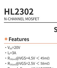
Ausschnitt eines Datenblatts für einen N-Channel MOSFET
HL2302 N-CHANNEL MOSFET Features • VDS=20V • ID=3A • RDS(on)@VGS=4.5V < 45mΩ • RDS(on)@VGS=2.5V < 58mΩ
in „Probleme beim Schalten eines Displays mit MOSFET und ESP32“ · Analoge Elektronik und Schaltungstechnik · · Screenshots
-
Bild
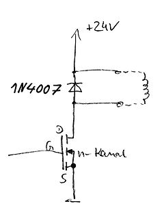
Handgezeichneter Schaltplan mit Diode und n-Kanal MOSFET
+24V 1N4007 n-Kanal G S
in „Unbekanntes Bauteil“ · Analoge Elektronik und Schaltungstechnik · · Schaltpläne
-
Bild
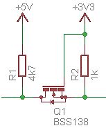
Schaltplan mit MOSFET Q1 BSS138
+5V +3V3 R1 4K7 R2 1K Q1 BSS138
in „1-Wire Frage: DS28e05 mit DS2480 interface chip auslesen“ · Mikrocontroller und Digitale Elektronik · · Schaltpläne
-
Bild
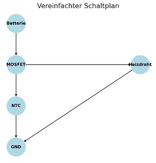
Vereinfachter Schaltplan mit Batterie, MOSFET, Heizdraht und NTC
Vereinfachter Schaltplan Batterie MOSFET Heizdraht NTC GND
in „Betreff: Hilfe bei der Erstellung einer Platine für ein kleines Angelzubehör-Projekt (KiCad)“ · Mikrocontroller und Digitale Elektronik · · Schaltpläne
-
Bild
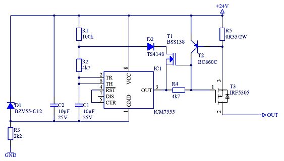
Schaltplan mit ICM7555 Timer und MOSFET-Treiberstufe
+24V, R5 0R33/2W, T1 BSS138, D2 TS4148, T2 BC860C, R4 4k7, T3 IRF5305, OUT, 1, 2, 3, IC1 ICM7555, 8 VCC, 6 TR, 7 TH, 4 RST, 5 DIS, 1 CTR, GND, C1 10uF 25V, C2 10uF 25V, R1 100k, R2 4k7, D1 BZV55-C12, R3 2k2
in „elektronische Sicherung“ · Analoge Elektronik und Schaltungstechnik · · Schaltpläne
-
Bild
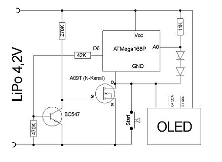
Schaltplan mit ATmega168P, OLED und MOSFET
LiPo 4,2V 270K 11K ATmega168P D6 A0 42K A09T (N-Kanal) BC547 D G S 470K C4 SDA C5 SCL OLED Start
in „Stromaufnahme weiter senken“ · Mikrocontroller und Digitale Elektronik · · Schaltpläne
-
Bild
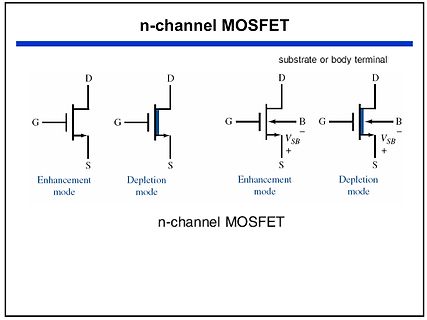
Symbole verschiedener n-Kanal MOSFET Typen
n-channel MOSFET substrate or body terminal D G S Enhancement mode Depletion mode B VSB
in „Schaltung mit 2 N-Kanal Mosfet“ · Analoge Elektronik und Schaltungstechnik · · Diagramme
-
Bild
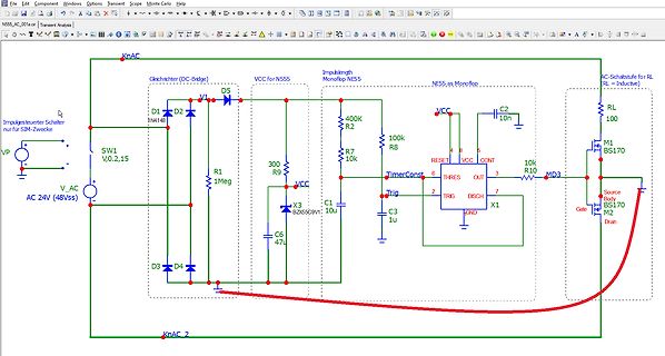
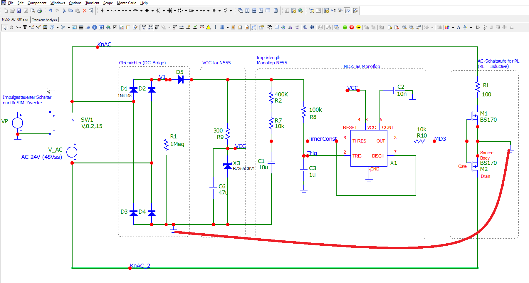
Schaltplan einer Impulsteuer Schaltung mit NE555 und MOSFET
File Edit Component Windows Options Transient Analysis Scope Monte Carlo Help N555_AC_001a Transient Analysis KnAC Gleichrichter (DC-Bridge) D1 D2 V1 3N4148 D5 VCC for N555 Impulslength Monoflop NE555 400K R2 100K R8 7k R7 10k C2 10n NE555 as Monoflop VCC RESET THRES OUT CONT 10k R10 MD3 300 R9 VCC X3 BZX55C9V1 C1 10u Trig TimerConst C3 1u X1 TRIG DISCH GND 1Meg V_AC AC 24V (48Vss) SW1 V0,2,15 D3 D4 KnAC 2 AC-Stufe fur RL RL = Inductive M1 BS170 Source Body M2 Dran Gate BS170
in „Mosfets als Klein-(wechsel)-spannung-Schalter“ · Analoge Elektronik und Schaltungstechnik · · Screenshots
-
Bild
Datenblatt eines N-Channel Enhancement Mode MOSFET
HYG060N08NS1D/U/V N-Channel Enhancement Mode MOSFET Feature 80V/80A RDS(ON)=5.7mΩ(typ.)@VGS = 10V 100% Avalanche Tested Reliable and Rugged Pin Description G D S D D Ordering and Marking Information D: TO-252-2L U: TO-251-3L V: TO-251-3S G060N08 XYMXXXXXXX
in „Anderer Source-Drain Widerstand bei Mosfet. Defekt?“ · Analoge Elektronik und Schaltungstechnik · · Screenshots
-
Bild
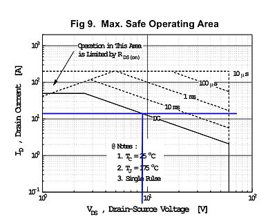
Diagramm der maximalen sicheren Arbeitsbereichs (SOA) eines MOSFETs
Fig 9. Max. Safe Operating Area Operation in This Area is Limited by RDS(on) ID, Drain Current [A] 10 µs 100 µs 1 ms 10 ms DC @ Notes : 1. TC = 25 °C 2. TJ = 175 °C 3. Single Pulse VDs, Drain-Source Voltage [V]
in „Reverse Voltage Protection“ · Analoge Elektronik und Schaltungstechnik · · Diagramme
-
Bild
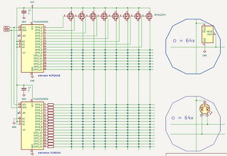
Schaltplan mit MOSFETs und I2C-Erweiterern
VCC, GND, SCL, SDA, INT, A0, A1, A2, U?, PI4IOE5V9555, GPIO_0 bis GPIO_15, IRLML2244, alternative MCP23018, C7, TLC59116, TLE 4913, VOUT, O = 64x
in „Schachbrettposition Erkennung“ · Mikrocontroller und Digitale Elektronik · · Schaltpläne
-
Bild
Maximum Safe Operating Area Diagramm eines MOSFETs
100 10 1 0.1 0.01 -ID, Drain-to-Source Current (A) OPERATION IN THIS AREA LIMITED BY RDS(on) 100µsec 1msec 10msec TA = 25°C Tj = 150°C Single Pulse -VDS, Drain-to-Source Voltage (V) 0 1 10 100 Fig 8. Maximum Safe Operating Area www.irf.com
in „Verpolungsschutz via MOSFET - ESD etc?“ · Analoge Elektronik und Schaltungstechnik · · Diagramme
-
Bild
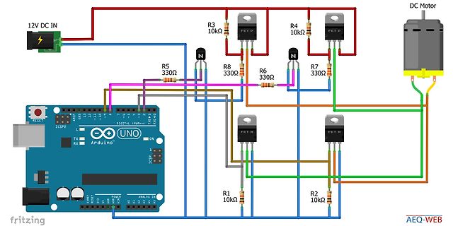
Fritzing-Schaltplan Arduino mit DC-Motor und MOSFETs
12V DC IN, R3 10kΩ, R4 10kΩ, FET P, DC Motor, R5 330Ω, R6 330Ω, R7 330Ω, R8 330Ω, UNO, Arduino, DIGITAL (PWM), ICSP2, TX, RX, FET N, R1 10kΩ, R2 10kΩ, AEQ-WEB, fritzing
in „Ansteuerung Motoren mit H-Brücke“ · Analoge Elektronik und Schaltungstechnik · · Schaltpläne
-
Bild
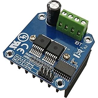
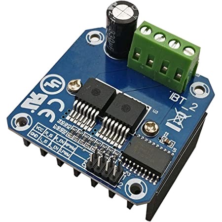
IBT_2 Motortreiber-Modul mit MOSFETs und Elektrolytkondensator
330uF, IBT_2, VCC, GND, R_S, L_S, EN, RPWM, LPWM, R5, 1, 2, 3, 5
in „Mit BTS7960 bremsen“ · Analoge Elektronik und Schaltungstechnik · · Platinenfotos
-
Bild
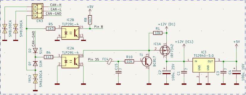
Schaltplan einer CAN-Bus Isolierung mit Optokopplern und MOSFET
CAN-H, CAN-L, CAN-GND, CN3, R5 1k3, TLP291-4, IC2B, 14, 13, +5V, R8 4k7, D2, SMBJ30CA, R4 1k3, TLP291-4, IC2A, 16, 15, 2, 1, SMBJ30CA, TRS2, Pin 35 FE4, R10 10k, T1, BC817, C15, C2 100u, IC1, IRF7342, +12V, GND, GND, IC3, TS2940-5.0, C3, +5V, C4 100u 16V
in „Ansteuerung einer Anzeigetafel - Federal Vama Traffic Storm“ · Fahrzeugelektronik · · Schaltpläne