Weil dann eine Wicklung mehr dazu kommt. Korrektur: Sind zwei unterschiedliche Wicklungen. quasi low und high wie beim Lüftermotor. Es wird jeweils nur eine Wicklung bestromt.
dann eine Wicklung mehr dazu kommt. > > Korrektur: Sind zwei unterschiedliche Wicklungen. quasi low und high wie > beim Lüftermotor. > > Es wird jeweils nur eine Wicklung bestromt. Unsinn.
actual_BJT_FET_leakage.pdf eventuell hilft https://www.vishay.com/docs/66597/sip32431.pdf 10 pA, Ultra Low Leakage and Quiescent Current, Load Switch with Reverse Blocking, 1.5-5.5V unter 0.2 Ohm
schrieb im Beitrag #7849520: > Wenn man z.B. ins Datasheet vom SN74AUP1G04 schaut findet man: > Low Static-Power Consumption (Icc = 0.9 μA Max) Schau dich eventuell mal bei neueren µC um: z.B.: STM32U0xx - https://www.st.com/en/microcontrollers-microprocessors/stm32-ultra-low-power-mcus.html
determined by the fre- used to advantage in the normal manner. Assuming these quency of oscillation; the lower the frequency the more sta- five inverters can be used elsewhere in the system, Figure 6 bility and vice versa. This is because propagation delay and must represent the ultimate in low gate count oscillators
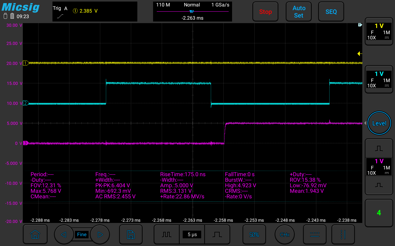
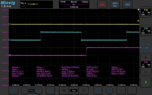
ns FallTime:0 s +Duty:--- FOV:12.31 % -Width:--- BurstW:--- ROV:76.92 mV Max:5.768 V PK-K:6.404 V High:4.923 V Low:76.92 mV CMean:--- Min:-692.3 mV CRMS:--- AC RMS:2.455 V +Rate:22.86 MV/s Mean:1.943 V -2.288 ms -2.273 ms -2.268 ms -2.263 ms -2.258 ms -2.253 ms -2.248 ms -2.243 ms -2.238 ms Fine 5 µs
LCD_send_DATA_byte(0x00); // Column Address Set (2Ah) LCD_send_CMD_byte(0x2A); LCD_send_DATA_byte(0x00); // Start high LCD_send_DATA_byte(u8_col_start); // Start low LCD_send_DATA_byte(0x00); // End high LCD_send_DATA_byte(u8_col_end); // End low // Row Address Set (2Bh) LCD_send_CMD_byte(0x2B); LCD_send_DATA_byte(0x00); // Start high LCD_send_DATA_byte(u8_row_start); // Start low LCD_send_DATA_byte(0x00); // End high LCD_send_DATA_byte(u8_row_end); // End low // Memory Write (2Ch) LCD_send_CMD_byte(0x2C); // send the pixels int
Unit Supply Voltage for Logic VCI Note 2.8 3.0 3.3 V Supply Voltage for Display VCC - 14 14.5 15 V High Level Input VIH - 0.8×VCI - VCI V - 0 - 0.2×VCI Low Level Input VIL V High Level Output VOH - 0.9×VCI - VCI V Low Level Output VOL - 0 - 0.1×VDDIO V 50% Check Board operating Current VCC =14.5V 23 24
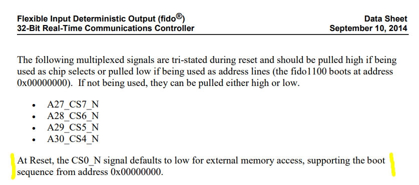
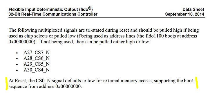
September 10, 2014
The following multiplexed signals are tri-stated during reset and should be pulled high if being used as chip selects or pulled low if being used as address lines (the fido100 boots at address 0x00000000). If not being used, they can be pulled either high or low.
A27_CS7_N
A28_CS6_N
A29_CS5_N
A30_CS4_N
At Reset, the CS0_N signal defaults to low for external memory access, supporting the boot sequence from address 0x00000000.
Hast du die Eingänge der unbenutzen Gatter auf high oder low gelegt? Wenn die offen sind könnte das die Stromaufnahme erklären.
Georg S. schrieb im Beitrag #7848643: > Hast du die Eingänge der unbenutzen Gatter auf high oder low gelegt? Es *ist* nur ein Gatter! Uwe B. schrieb im Beitrag #7848648: > Wenn, dann Single LVC1Gu04 Unbuffered Inverter Nicht für diese Art von Oszillator. Da *muß* es ein Schmitt-Trigger
STripFET™ Power MOSFET Features 2N7000 V60 V < 5 Ω(@10V) 0.35 A 3 2N7002 60 V < 5 Ω(@10V) 0.20 A 2 s ) ■ Low Qg 1 c t( ■ Low threshold drive SOT23-3L d TO-92 Application P r o ■ Switching applications te Description o le This Power MOSFET is the second generation of s strip-based process. The resulting transistore”e 1. Internal schematic diagram shows extremely high packing denssty for low on- less critical alignment stepc therefore aics and remarkable manufacturond reproducibility. P r te o le SOT23-3L TO-92 b s O Table 1. Device summary Or2N7000des 2N7000Gg PTO
all flip-flops simultaneously. The D-input that meets the set-up and hold time requirements on the LOW-to-HIGH clock transition will be stored in the flip-flop and appear at the Q output. A LOW on MR causes the flip-flops and outputs to be reset LOW. Inputs include clamp diodes. This enables the use
outputs (Y0 to Y7). The device features three enable inputs (E1, E2 and E3). Every output will be HIGH unless E1 and E2 are LOW and E3 is HIGH. This multiple enable function allows easy parallel expansion to a 1-of-32 (5 to 32 lines) decoder with just four '138 ICs and one inverter. The '138 can be used
Conditions 25 C 40 C to +85 C 40 C to +125 C Unit Min Typ Max Min Max Min Max 74HC11 V IH HIGH-level V CC = 2.0 V 1.5 1.2 - 1.5 - 1.5 - V input voltage V = 4.5 V 3.15 2.4 - 3.15 - 3.15 - V CC V CC = 6.0 V 4.2 3.2 - 4.2 - 4.2 - V V IL LOW-level V CC = 2.0 V - 0.8 0.5 - 0.5 - 0.5 V input voltage
Nexperia 74HC08; 74HCT08 Quad 2-input AND gate 6. Functional description Table 3. Function table H = HIGH voltage level; L = LOW voltage level; X = don’t care. Input Output nA nB nY L L L L H L H L L H H H 7. Limiting values Table 4. Limiting values In accordance with the Absolute Maximum Rating System
Light-emitting surface suitable for legend attachment per Application Note 1012 HLCP-x100 series designed for low current operation Bicolor devices available Applications Business machine message annunciators Telecommunications indicators Front panel process status indicators PC board identifiers Bar
necessary precautions. 6.3 Recommended Operating Conditions MIN MAX UNIT VCC Supply voltage 2.5 6 V V High-level input voltage 0.7 × V V + 0.5 V IH CC CC VIL Low-level input voltage –0.5 0.3 × CC V OH High-level output current –1 mA OL Low-level output current 25 mA T Operating free-air temperature –40 85
Matrix Characters The DLX413X/DLX713X are single digit 5 x 7 dot DLO4135/DLG4137: 10.92 mm (0.43") High matrix Intelligent Display devices. The DLX413X DLO7135/DLG7137: 17.27 mm (0.68") High character is 10.92 mm (0.43") high. The DLX713X Wide Viewing Angle ± 75° character is 17.27 mm (0.68") high. The
conditions All transactions begin with a START (S) and are terminated by a STOP (P) (see Figure 5). A HIGH to LOW transition on the SDA line while SCL is HIGH defines a START condition. A LOW to HIGH transition on the SDA line while SCL is HIGH defines a STOP condition. SDA SCL S P START condition STOP condition
Acknowledge bits if an internal programming cycle is in progress. Both data and clock lines remain high. A device that acknowledges must pull down the SDA line during the Acknowledge clock pulse in such a way 4.2 Start Data Transfer (B) that the SDAline is stable-low during the high period of A high-to-low
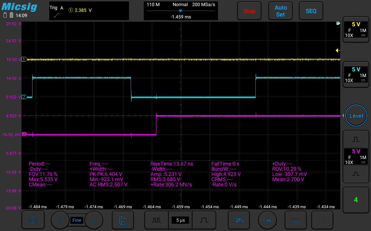
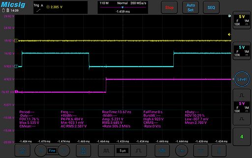
19.92 V 14.92 V 9.923 V 5 V 1 M 10X 5 V 1 M 10X 4.923 V Level -76.92 mV -5.077 V 5 V 1 M -Rate:0 V/s Low:-307.7 mV -10.08 V -14.59 ms -1.479 ms -1.459 ms -1.439 ms -14.09 14:09 Period: Duty: FOV:11.76 % Max:5.535 V CMean:-- Freq.: +Width:-- PK-PK:6.404 V Min:-923.1 mV RMS:3.685 V AC RMS:2.507 V RiseTime:13.67 ns -Width:-- Amp:.5231 V BurstW: High:4.923 V CRMS: FallTime:0 s -20.08 V -15.08 V -1.484 ms -1.474 ms -1.464 ms -1.454 ms -1.444 ms -1.434 ms Fine 5 µs 50% CHx
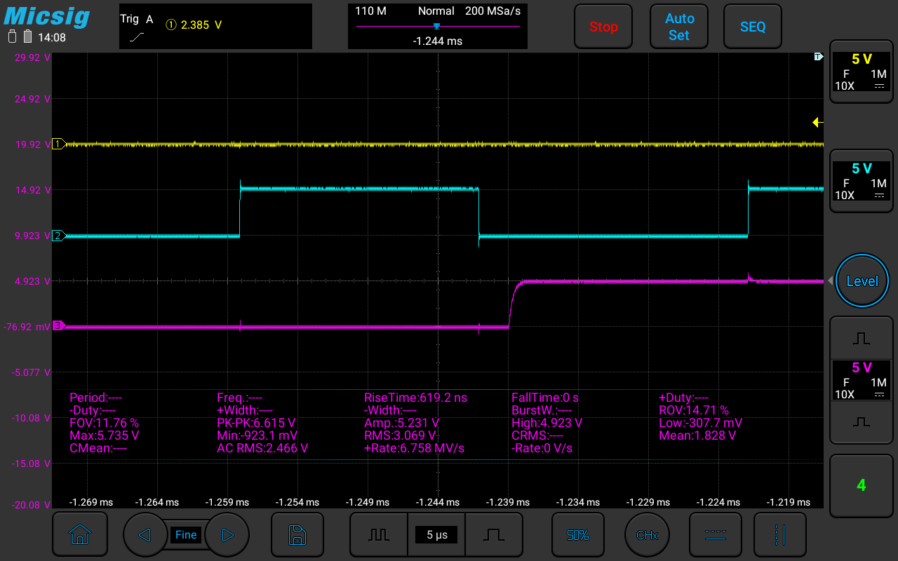
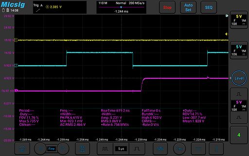
RiseTime:619.2 ns FallTime:0 s +Duty:--- FOV:11.76 % +Width:--- BurstW:--- ROV:14.71 % Amp.:5.231 V High:4.923 V Low:-307.7 mV Max:5.735 V Min:-923.1 mV Mean:1.828 V RMS:3.069 V CRMS:--- -20.08 V AC RMS:2.466 V -Rate:6.758 MV/s -1.269 ms -1.264 ms -1.259 ms -1.254 ms -1.249 ms -1.244 ms -1.239 ms -1.234
Start-Taste, eine definierte Zeit runter zählt und danach abschaltet. Das geschieht, indem Port6 von LOW auf HIGH wechselt. Die Bauteile wurden mehr oder weniger willkürlich gewählt, da ich diese gerade zur Hand hatte. Die Schaltung funktioniert soweit einwandfrei, aber die Ruhestromaufnahme beträgt immerhin
Arduino Pro Mini Power Consumption: https://www.hackster.io/news/how-one-maker-built-an-ultra-low-power-arduino-pro-mini-6b5337997e91 https://www.iot-experiments.com/arduino-pro-mini-power-consumption/ https://andreasrohner.at/posts/Electronics/How-to-modify-an-Arduino-Pro-Mini-clone-for-low-power-consumption
And Technology Co.,Ltd. Add: 50m to the North from intersection of Wolong Street and Yuquan Road,High-Tech Zone, Weifang,China 261061 Tel :+86-0536-8869515 Fax:+86-0536-8669360 Mob:+86-13361538912 MSN: qinyitec@hotmail.com Skype : qinyitec Google Talk :qinyitec@gmail.com E-mail: dave@qinyitec.com ;
at high frequencies so that R may decouple a highly capacitive load and reduce the Q of the (1) series resonant circuit due to capacitive load. Also provides a low impedance at low frequencies to short out
Kitchen Radios Band III (162 - 240 MHz) Band IV/V (470 - 960 MHz) KEY BENEFITS L-Band (1450 - 1675 MHz) High performance architecture Support for global broadcast standards Low Noise, high linearity DVB-T, ISDB-T, DTMB DVB-H, CMMB, T-DMB, T-MMB Adaptive FlexiRF“ architecture AM, FM, DRM, DAB, HD Supports zero IF and low IF systems Enables low-cost OEM platform strategy Low external component count Global solution using one tuner Minimal external SMDs required Performance margin to standards Small footprint package
VN5E016AH-E Table 7. Logic Inputs Symbol Parameter Test conditions Min. Typ. Max. Unit V IL Input low level voltage - - 0.9 V IL Low level input current VIN = 0.9V 1 - - µA V IH Input high level voltage 2.1 - - V IH High level input current VIN = 2.1V - - 10 µA VI(hyst)Input hysteresis voltage 0.25 - - V IIN= 1mA 5.5 - 7 VICL Input clamp voltage V IIN= -1mA - -0.7 - VCSDL CS_DIS low level voltage - - 0.9 V ICSDL Low level CS_DIS current VCSD = 0.9V 1 - - µA V CS_DIS high level voltage 2.1 - - V CSDH I High level CS_DIS current V = 2.1V - - 10 µA CSDH CSD V CS_DIS hysteresis voltage
device n LINEAR CURRENT LIMITATION n THERMAL SHUT DOWN n SHORT CIRCUIT PROTECTION n INTEGRATED CLAMP n LOW CURRENT DRAWN FROM INPUT PIN n DIAGNOSTIC FEEDBACK THROUGH INPUT PIN n ESD PROTECTION SO-8 n DIRECT ACCESS TO THE GATE OF THE POWER MOSFET (ANALOG DRIVING) n COMPATIBLE WITH STANDARD POWER MOSFET Technology
each channel. Table 10. Logic Input Symbol Parameter Test conditions Min. Typ. Max. Unit V IL Input low level 0.9 V IL Low level input current V IN= 0.9V 1 µA V IH Input high level 2.1 V IH High level input current V IN= 2.1V 10 µA VI(hyst)Input hysteresis voltage 0.25 V IN= 1mA 5.5 7 V VICL Input clamp voltage I = -1mA -0.7 V IN V STAT_DIS low level voltage 0.9 V SDL SDL Low level STAT_DIS current V SD=0.9V 1 µA V SDH STAT_DIS high level voltage 2.1 V SDH High level STAT_DIS current V SD=2.1V 10 µA VSD(hyst)STAT_DIS hysteresis voltage 0.25
3signed ■ Undervoltage and overvoltage shutdown driving any type of multiple load with one side ■ Very low standby currentn O connected to ground. ■ Reverse battery protection ) - device against low energy spikes (see ISO7637 t( s transient compatibility table). Active current u c automatic restart protects
VN920SP-E High-side driver Features Type R I V DS(on) OUT CC VN920SP-E 15 mΩ 30 A 36 V ® ■ ECOPACK : lead free and RoHS compliant ■ Automotive Grade: compliance with AEC guidelines ■ Very low standby current Description
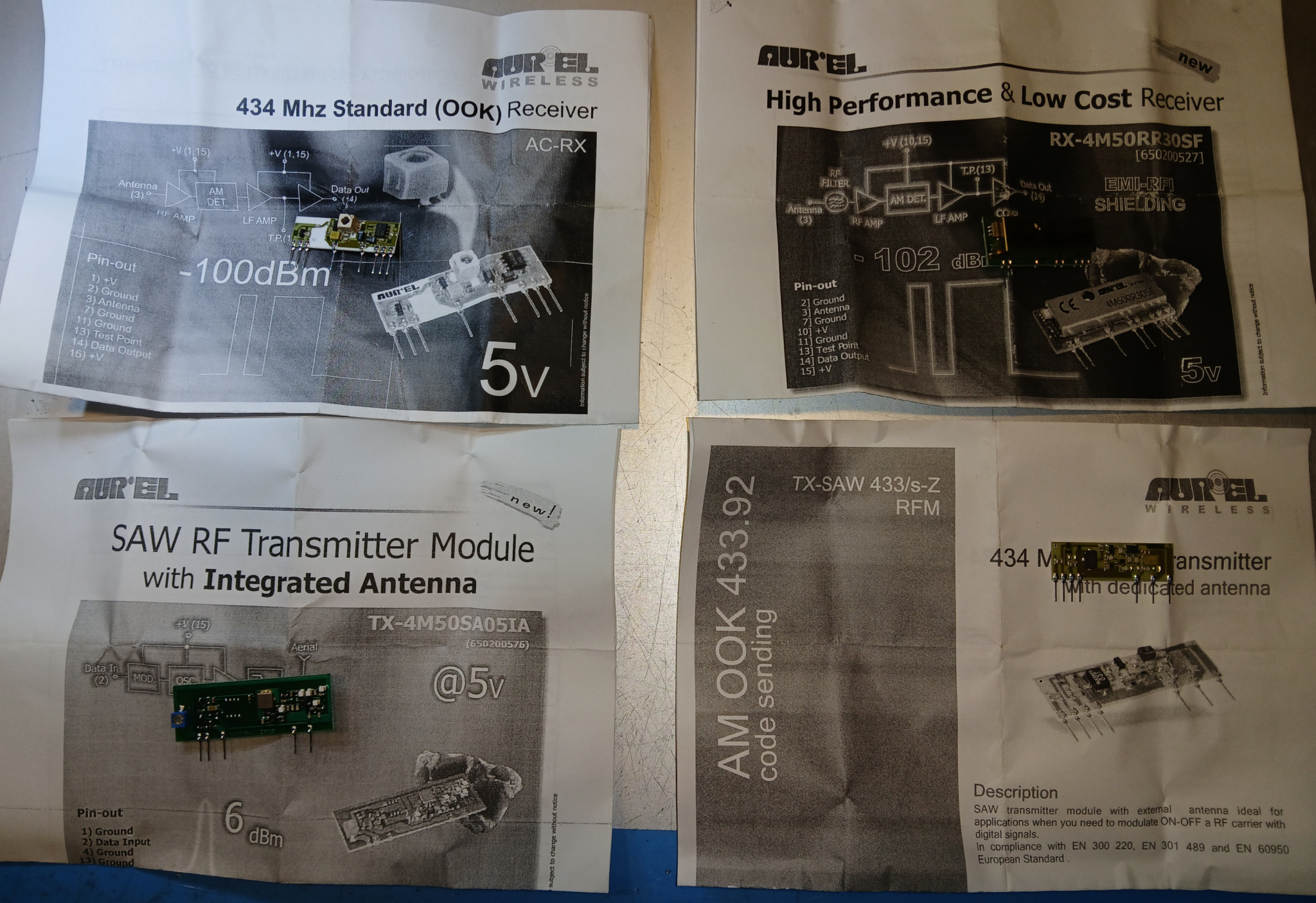
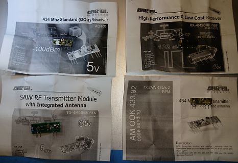
(3) AM DET LF AMP Data Out (4) Pin-out 1) +V 2) Ground 3) Antenna 4) Data Output 5) +V -100dBm 5v High Performance & Low Cost Receiver RX-4M50RP30SF AUR EL WIRELESS TX-SAW 433/s-Z RFM 434 MHz transmitter with dedicated antenna SAW RF Transmitter Module with Integrated Antenna TX-4M50SA051A AM OOK 433.92
Property of Lite-On Only FEATURES ▯0.39 inch (10.0 mm) DIGIT HEIGHT ▯CONTINUOUS UNIFORM SEGMENTS ▯LOW POWER REQUIREMENT ▯EXCELLENT CHARACTERS APPEARANCE ▯HIGH BRIGHTNESS & HIGH CONTRAST ▯WIDE VIEWING ANGLE ▯SOLID STATE RELIABILITY ▯CATEGORIZED FOR LUMINOUS INTENSITY DESCRIPTION The LTS-4812SKR-P is
UL 94 V-0) Epoxy resin sealing (UL 94 V-0) Features Capacitance values up 0.47 μF to 170 μF High CV product, compact Good self-healing properties Over-voltage capability Low losses with high current capability High reliability Long useful life RoHS-compatible UL 810 construction
deshalb vom µC leicht ermittelt werden kann, ob da was wechselt. Denn wenn der Ausgang *dauerhaft* high oder auch low ist, dann ist irgendwas faul oder kaputt. Bei den anderen Schaltungen, die aus einer Wechselspannung ein dauerhaftes Schaltsignal machen, wird ein Fehler nicht erkannt, wenn der es schafft
nicht nur detektieren, sondern auch noch entsprechend reagieren. Was soll die Maschine machen wenn es Low ist, was wenn Dauerhigh, was wenn Pulse kommen. Wie die Pulse auswerten? Interrupts? Zähler? Soll man auf die Frequenz achten? Evtl. wird die Schaltung auch mal anderswo eingesetzt, da ist aber ein
Funktion zur Steuerung des Gartensprengers def schalte_gartensprenger_an(): GPIO.output(15, GPIO.HIGH) # GPIO-Pin 15 aktivieren print("Gartensprenger aktiviert!") time.sleep(5) # Sprinkler für 5 Sekunden aktiv halten GPIO.output(15, GPIO.LOW) # GPIO-Pin 15 deaktivieren print("
Großkatzen wenn der Löwe zweimal klingelt Es gibt keine genauen Angaben zum Schalter, jedenfalls ist das rein digital, Löwe steht auf der Matte oder nicht.
bei der Battery University nachgucken: https://batteryuniversity.com/article/bu-410-charging-at-high-and-low-temperatures Betrifft vor allem das Laden.
bei der Battery University nachgucken: > https://batteryuniversity.com/article/bu-410-charging-at-high-and-low-temperatures > Betrifft vor allem das Laden. Danke sehr! Wieder ein paar Informationen mehr die noch nicht bekannt sind und bei Bedarf weiterhelfen.
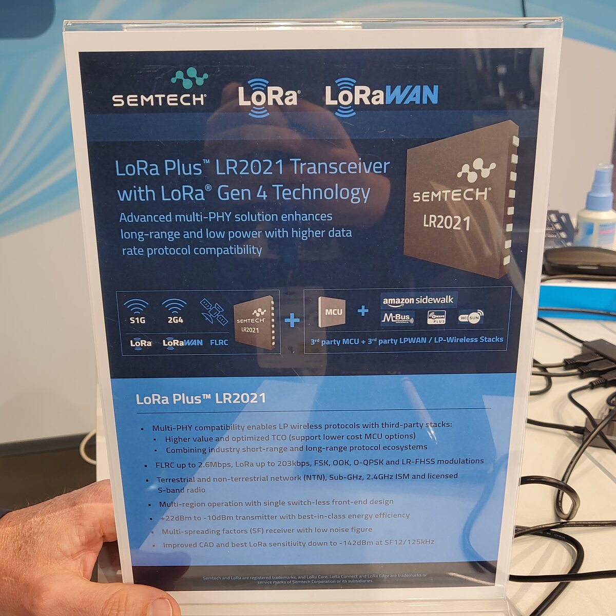
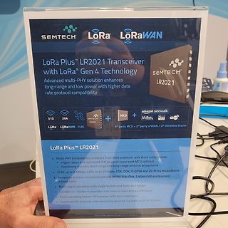
LR2021 Transceiver with LoRa® Gen 4 Technology Advanced multi-PHY solution enhances long-range and low power with higher data rate protocol compatibility SEMTECH LR2021 5G 2G4 LoRa LoRaWAN FLRC MCU + amazon sidewalk M-Bus FLIRC LoRaWAN 3rd party MCU + 3rd party LPWAN / LP-Wireless Stacks LoRa Plus™ LR2021 Multi-PHY compatibility enables LP wireless protocols with third-party stacks; Higher value and optimized TCO (support lower cost MCU options); Combining industry short-range and long-range protocol ecosystems; FLRC up to 2.6Mbps, LoRa up to 203kbps, FSK, OOK, QPSK and LR-FHSS modulations
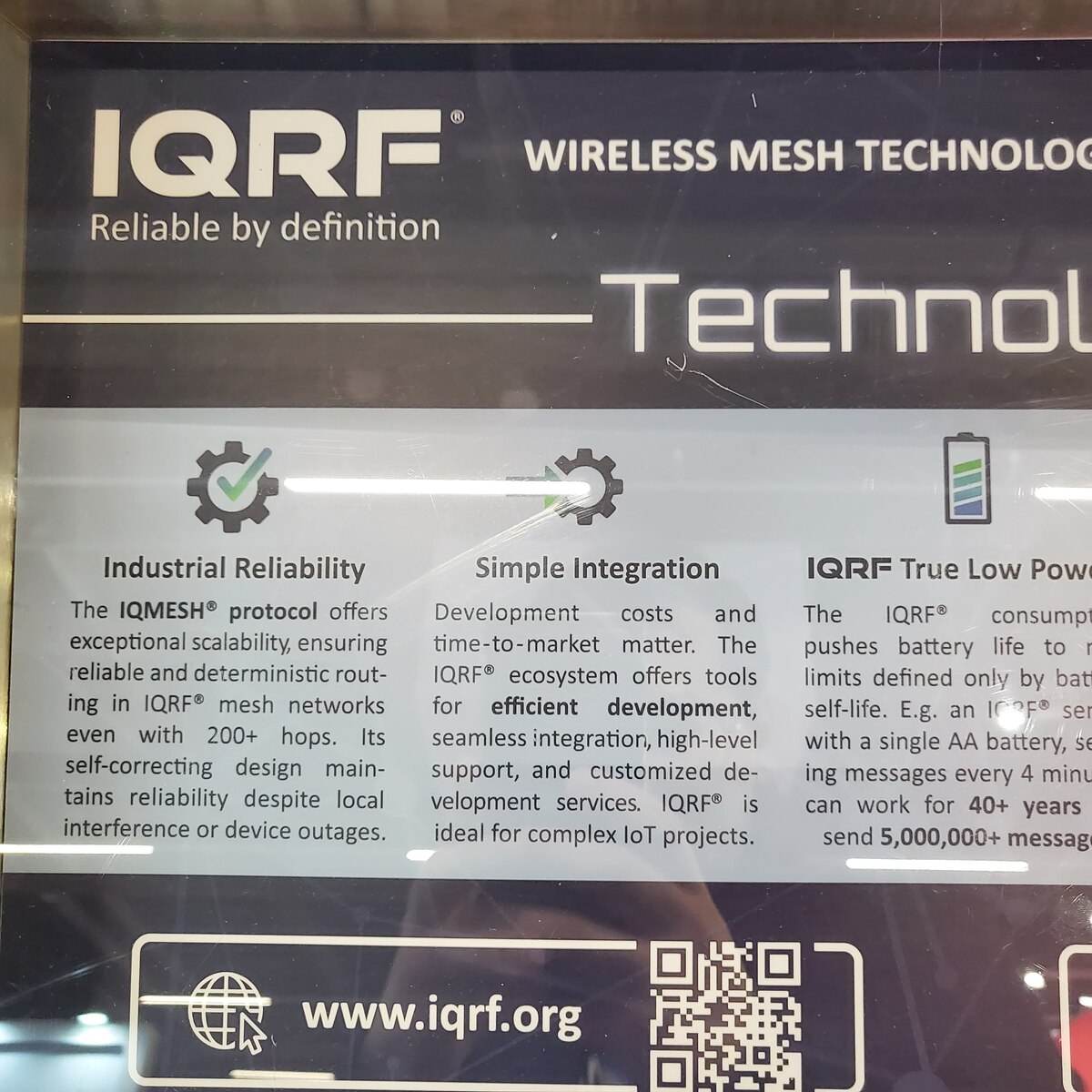
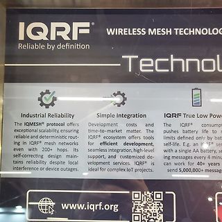
time-to-market matter. The IQRF ecosystem offers tools for efficient development, seamless integration, high-level support, and customized development services. IQRF is ideal for complex IoT projects. IQRF True Low Power The IQRF consumption pushes battery life to remarkable limits defined only by battery
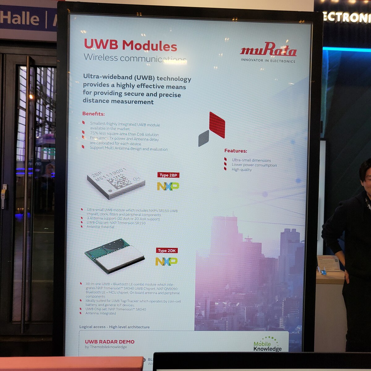
Support: Multi-Antenna design and evaluation
Type 2BP
MS-1190D1
NXP
Features:
Ultra-small dimensions
Lower power consumption
High quality
Ultra small UWB module which includes NXP SR150 UWB chipset, lock, filters and peripheral components
Antenna support (3D AoA or 2D AoA support)
UWB Direction: NXP Trimension
clock that RXF# and RD# are both low. Note that the OE# pin must be driven low at least 1 clock period before asserting RD# low. When high, do not write data into the FIFO. When low, data can be written into the FIFO by driving WR# low
Time SU:STO 2.6 — — µs Data Hold Time HD:DAT 0 — — µs Data Setup Time SU:DAT 1.3 — — µs Detect Clock Low Timeout t 25 — — ms TIMEOUT Clock Low Period LOW 1.3 — — µs Clock High Period HIGH 2.6 — 503 µs Note: 1.The minimum SMBus frequency is limited by the maximum Clock High Period requirement of the SMBus
1 1 1 0 2 1 1 3 (Highest) 47 4164G–SCR–07/06 A low-priority interrupt can be interrupted by a high priority interrupt, but not by another low-priority interrupt. A high-priority interrupt can’t be interrupted by any other
, geht die Abstimmung so wie ich mir das vorgestellt habe. Offensichtlich haben diese Widerstände High und Low so verbeult dass der Pico Fehler machte. So ärgerlich der Fehler ist, aber ich dürfte nicht der einzige sein der dieses Teil in dieser Schaltung verbaut hat. Er war auf der Webseite für den
das noch einstellen lässt. Danke, ich habe das unter "Encoder Resolution" gefunden .Habe das von "Low" auf "High" gestellt. Jetzt passt das wieder.

 Bild
Bild
 Bild
Bild
 Bild
Bild
 Bild
Bild
 Bild
Bild
 Bild
Bild
 Bild
Bild
 Bild
Bild
 Bild
Bild
 Bild
Bild