e E C e E X d X d - i - i F t F t D o D o r r P ! P ! W W O O N N Y Y U U B B t o t o k k w c w c l i l i w C m w C m o o w w . c . c . p e . p e d g d g f - n f - n x c h a x c h a Selbstkonfektionierbarer Stecker und Buchse Stecker SLS1-S Starr, Ø 1 mm, für die Selbstmontage von Messleitungen. Lötanschluss
coefficient curve STR-X6759N Ta=25℃ MOSFETA.S.O.Curve Single pluse 100 100 ) (80 n 0.1ms c f 10 o t c60 e i ] u 1ms a D C d I i e r DeterminedbyOn-Reststacen t40 D r 1 p ApplyA.S.Otemperaturecoefficient e .20 fromtheleftgraphtothiscurvefor . evaluatingactualoperations' safety . A 0.1 0 0 20 40 60 80 100
border-top:2px solid;border-bottom:solid;border-right:solid;"background-color:#DCE6F1" width="66"|H3 l ABC style="border-left:2px;border-top:solid;border-right:solid;"background-color:#EBF1DE" height="15" |Z1 Test style="border:1px solid;"background-color:#FCD5B4"|X AB Line DEF style="border-left:2px;
colspan="2" | 3V3 only colspan="2" | 5V & 3V3 IC1, (IC3) LT1933 LT1933S6 LT 1933 ES6 2,80 € 1 2,80 € 2 5,60 € 1 12,80 € Hier geht es zu dem Reichelt-Warenkorb mit den benötigten Bauteilen. Und hier geht es zu einem anderen Warenkorb von Reichelt. = svg-Grafik = = Bildbeispiel = Hier steht die Einleitung. Etwas
Collector Current 10 IF= 50 mA 110 t 100 0 ) 20 mA e A = 1 mm A u 90 ( 10 mA C 80 n 1 o r c 70 s u 5 mA l 60 r C t e 50 e 2 mA t o 0.1 l 40 C R 30 C 1 mA - I r 20 IC 10 0.01 0 0.1 1 10 100 - 0.5 0.- 0.3- 0- 0.10 0.1 0.2 0.30.4 0.5 s - Displacement (mm) 96 12067 V CE - Collector Emitter Voltage (V) 96 12005
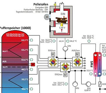
Pelletofen
Freigabe: EIN
Fehlerfreier Betrieb: EIN
Tagesbetriebszeit: 0 Std 59 Min
EIN
5,60 V
Pufferspeicher (1000l)
WW-Anforderung: AUS
FBH-Anforderung: AUS
63,3 °C
Ist: 55,9 °C
Soll: 55,0 °C
63,2 °C
64,2 °C
Δ8,5K
EIN/aus
AUS/aus
Ist: 53,1 °C
61,6 °C
44,5 °C
Soll: 50,0 °C
AUS
32,0 °C
Ist:
Benedikt L. schrieb im Beitrag #7851645: > WS2812 LEDs. einzeln addressierbar und problemlos. Das Problem ist, die haben keinen Diffusor, d.h. es sind winzige Punktquellen, die leicht blenden. Auch sind die
V40511 (um den handelt es sich ja wohl) sind es eher 100Ω. Mit Deinen Zahlen komme ich nur auf 50 bis 60Ohm. Ich stelle mal ein weiteres Beispiel vor, welches ohne V40511 die LED–Balken mittels eines Transistors schaltet. (Siehe Anhang) Die je 6 LED in Parallelschaltung stellen jeweils einen Segmentbalken
Arbeitstemperaturbereich °C -40 bis +125 Epoxy Wärmeleitfähigkeit W/(m.K) 1,7 Abemessungen in mm 11.73 max. L = 240 mm +/- 5 mm L 5 mm +/- 1 mm 4 mm +/- 0.1 mm A A = M4 Loch 2 0 2 s e u r p e _ 1 3 0 T - T Änderungen und Irrtümer vorbehalten E Temperatursensor ETP-RT Bestellinformation für Standard-Lager-Modelle
Current vs. Ambient Temperature 0° 10° 20° 100 30° ) µ t t e s 40° r 10 e 1.0 C I h e i t 0.9 50° L l s V = 5 V R 0.8 60° e 1.0 CE l e λ = 950 nm r R I 0.7 70° -r 80° I 0.1 0.6 0.4 0.2 0 0.2 0.4 0.6 0.01 0.1 1 10 18234 16055 E - Irradiance (mW/cm²) e Fig. 6 - Relative Radiant Intensity vs. Angular
λ typ. 600 nm S max Spectral range of sensitivity λ10% typ. 400 ... 950 nm Dimensions of chip area L x W typ. 0.75 x 0.75 mm x mm Radiant sensitive area A typ. 0.29 mm² Half angle φ typ. 60 ° Dark current ICE0 typ. 6 nA VCE = 5 V; E = 0 max. 50 nA Collector-emitter saturation voltage ) VCEsat typ. 100
Oder vielleicht lässt sich ein TPS7A02 als Logik-Gate missbrauchen, der hat garantiert max Verbrauch <60nA, und enthält immerhin eine vollwertige Regelung, Komparatoren usw.
Clemens L. schrieb im Beitrag #7849872: > Niklas G. schrieb im Beitrag #7849791: >> Beim "Advanced Ultra-Low Power" IC heißt es 0.9µA, bei "Advanced CMOS" >> jedoch <50nA. Hä? > > 0.9 µA ist das Maximum
October 1974 S O s c i INTRODUCTION switches with finite propagation delays rather than as ampli- l fiers with 180˚ phase shift. It then becomes obvious that a “1” t This note describes several square wave oscillators that can chases itself around the ring and the network oscillates. o be built using
3.2 Line type : (As following drawing) Length Width Acceptable Q TY --- W≦0.02 Accept no dense 2.5 L≦3.0 0.02<W≦0.03 2 L≦2.5 0.03<W≦0.05 --- 0.05<W As round type 04 Polarizer bubbles If bubbles are visible,Size Φ Acceptable Q TY judge using black Φ≦0.20 Accept no dense spot specifications, 0.20<Φ≦0.50
2N7000 2N7002 N-channel 60 V, 1.8 Ω, 0.35 A, SOT23-3L, TO-92 STripFET™ Power MOSFET Features 2N7000 V60 V < 5 Ω(@10V) 0.35 A 3 2N7002 60 V < 5 Ω(@10V) 0.20 A 2 s ) ■ Low Qg 1 c t( ■ Low threshold drive SOT23-3L d TO-92 Application
lohnt es sich, die fünf Euro für eine Rolle von Vishay, ASJ oder Yageo auszugeben. Aber das sind fette 60% Mehrkosten, die sich der Händler spart. SMD-Widerstände sehen alle gleich aus, aber sie können 50 ppm oder 200 ppm/K Temperaturgang haben. Und es gibt sie mit 20% pulse overload rating, oder mit
sich, die fünf Euro für eine Rolle > von Vishay, ASJ oder Yageo auszugeben. Aber das sind fette 60% > Mehrkosten, die sich der Händler spart. Ein Sortiment hat man ja üblicherweise für Entwicklung, damit man mal alles Mögliche durchprobieren kann. Standardware ohne spezielle Eigenschaften ist
description [1] Table 3. Function table Operating modes Inputs Outputs MR CP Dn Qn Qn reset (clear) L X X L H load “1” H h H L load “0” H l L H [1] H = HIGH voltage level; h = HIGH voltage level one set-up time prior to the LOW-to-HIGH clock transition; L = LOW voltage level; l = LOW voltage level
demultiplexer; inverting 6. Functional description Table 3. Function table H = HIGH voltage level; L = LOW voltage level; X = don’t care. Control Input Output E1 E2 E3 A2 A1 A0 Y7 Y6 Y5 Y4 Y3 Y2 Y1 Y0 H X X X X X H H H H H H H H X H X X X L L L H L L L H H H H H H H L L L H H H H H H H L H L H L H H H H H L H H L H H H H H H L H H H H L L H H H L H H H H H L H H H L H H H H H H H L H L H H H H H H H H H L H H H H H H H 7. Limiting values Table 4. Limiting values In accordance with the Absolute Maximum Rating
reset; positive edge-trigger 6. Functional description Table 3. Function table H = HIGH voltage level; L = LOW voltage level; X = don’t care. Input Output nSD nRD nCP nD nQ nQ L H X X H L H L X X L H L L X X H H Table 4. Function table H = HIGH voltage level; L = LOW voltage level; X = don’t care; ↑ = LOW-to-HIGH
3-input AND gate 6. Functional description Table 3. Function selection[1] Input Output nA nB nC nY L X X L X L X L X X L L H H H H [1] H = HIGH voltage level; L = LOW voltage level; X = don’t care 7. Limiting values Table 4. Limiting values In accordance with the Absolute Maximum Rating System (IEC
74HCT08 Quad 2-input AND gate 6. Functional description Table 3. Function table H = HIGH voltage level; L = LOW voltage level; X = don’t care. Input Output nA nB nY L L L L H L H L L H H H 7. Limiting values Table 4. Limiting values In accordance with the Absolute Maximum Rating System (IEC 60134). Voltages
Ambient Temperature 1.2 35 d c A m 1.0 m30 Y - I A N S m E25 E 20.8 R T T U I A C20 S D0.6 D O I E I L L15 M A A L R0.4 W E O O10 I ( L T 0.2 A L X 5 E M R 0.0 0 0 5 10 15 20 25 30 0 10 20 30 40 50 60 70 80 90 FORWARD CURRENT- mA AMBIENT TEMPERATURE, TA - °C Broadcom AV02-4479EN 11 HLCP-A100/-B100/-C100
= 100 kHz SCL = VCC All I/Os unloaded 80 All I/Os unloaded 100 ) VCC = 5 V )70 ( m VCC= 5 V t 80 t60 e e u 60 r50 C C l l40 VCC= 2.5 V p 40 p30 S u VCC = 3.3 V VCC = 3.3 V S20 20 VCC = 2.5 V 10 0 0 −50 −25 0 25 50 75 100 125 −50 −25 0 25 50 75 100 125 Temperature (°C) Temperature (°C) Figure 1. Supply
multiplexers and switches may exceed this capacitance because they connect multiple paths together. s 1 4 e l r 0 4 g m 2 7 s a 0 f e u 6 e a 4 4 . l xxxxxxxxxxxxxxxxxxxxx xxxxxxxxxxxxxxxxxxxxxxxxxx xxxxxxx x x x xxxxxxxxxxxxxxxxxxxxxxxxxxxxxx xxxxxxxxxxxxxxxxxxx xx xx xxxxx xxxxxxxxxxxxxxxxxxxxxxxxxxx xxxxxxxxxxxxxxxxxxx
Packaging Specification located at http://www.microchip.com/packaging 4X ș1 R1 H R c SEATING PLANE C L ș (L1) 4X ș 1 DETAIL B Units MILLIMETERS Dimension Limits MIN NOM MAX Number of Terminals N 8 e Pitch 0.65 BSC Overall Height A – – 1.10 Standoff A1 0.00 – 0.15 Molded Package Thickness A2 0.75 0.85
Neodymmagnete in 2 Reihen rotieren, angetrieben durch einen Scheibenwischermotor, um einen Rührfisch in einem 60L Tank mitzuschleppen. Die Aluplatte, die den Deckel des Rührers bildet, wurde auch gut handwarm.
Sebastian L. schrieb im Beitrag #7847777: > Kann das etwas Positives bewirken Ja! Das wird bei großen Akkupacks (zB Elektroautos) auch genau so gemacht. Dadurch gleichen sich die parallel geschalteten Zellen
zurecht zu kommen. Ich habe die Menge der Batterien so gewählt, dass ich sie insg. seltenst unter 60-70% Ladestand bringe.
www.qinyitec.com SPECIFICATION 1.Product show : Description Model Photo Pressure sensor of E-cigarette C6027L-C104-RS 2.Characteristic: 1). ASIC design. 2). Low quiescent current in Power Saving Mode (<5uA). 3).Short Circuit Protection(SCP). 4.) Under voltage lock out(UVLO). 5). Over-temperature protection(OTP
Michael L. schrieb im Beitrag #7847675: > Wie? Du machst einen Thread wegen Spulenfiepen auf und am Ende teilst Du > mit, daß das Netzteil Schrott ist? Selten dämlich. Ich antworte nur auf Fragen und bekomme
Michael L. schrieb im Beitrag #7847688: > Willst Du mich auf den Arm nehmen? Sich bei einem offensichtlich > defekten Netzteil um Spulenfiepen Sorgen zu machen, ist ja wohl > unsinnig. Sieh zu, daß Du das
Output Power (Continuous Average) THD + N = 0.1% (max) f = 1 kHz; f = 20 kHz + − |V+| = |− | = 28V, L = 4Ω 68 60 W (min) |V | = |V | = 28V, L = 8Ω 38 30 W (min) |V | = |V | = 35V, L = 8Ω 50 W Peak P O Instantaneous Peak Output Power 135 W THD + N Total Harmonic Distortion Plus Noise 60W, R L 4Ω, % 30W
selbst. Philipp G. schrieb im Beitrag #7848130: > Der Lochraster bekommt dann beidseitig Plastik 60, Das halte ich für überflüssig. Ist der Lack Deiner Widerstände gegen dessen Lösungsmittel beständig? Bauform B. schrieb im Beitrag #7848148: > Muss das sein? Die meisten Schaltungen kommen doch
R. L. schrieb im Beitrag #7848969: > die Lötbarkeit leidet nach 10 Jahren, d.h. die Gefahr von > schlechte Lötstellen steigt. Es heißt "schlechten", Baumschule? Quatsch ist es obendrein, hier lassen
mechanical data Data book mm Ref. dim Nom. Min. Max. A - 2.20 2.40 A1 - 0.90 1.10 A2 - 0.03 0.23 b - 0.45 0.60 b4 - 5.20 5.40 c - 0.45 0.60 c2 - 0.48 0.60 D - 6.00 6.20 D1 5.10 - - E - 6.40 6.60 E1 5.20 - - e 0.85 - - e1 - 1.60 1.80 e2 - 3.30 3.50 e3 - 5.00 5.20 H - 9.35 10.10 L - 1 - (L1) 2.80 - - L2 0.80 - - L4 - 0.60 1.00 R 0.20 - - V2 - 0° 8° Doc ID 15994 Rev 5 33/37 Package and packing information VN5E016AH-E 5.2 Packing information The devices can be packed in tube or tape and reel shipments (see Table
rr Reverse Recovery Time SD =0.5A; dI/dt=6A/ s 205 ns Q Reverse Recovery Charge 100 C rr VDD=30V; L=200 H RRM Reverse Recovery Current (see test circuit, figure 2) 0.75 A PROTECTIONS (-40°C < T j< 150°C, unless otherwise specified) Symbol Parameter Test Conditions Min Typ Max Unit Ilim Drain Current
tf r t INPUT d(on) td(off) t Table 11. Truth table Conditions INPUTn OUTPUTn STATUSn (V SD=0V)(1) L L H Normal operation H H H L L H Overtemperature H L L Undervoltage L L X H L X H X H Overload & (no power limitation) Short circuit to GND H Cycling L (power limitation) (2) L H L Output voltage >OL H H H L L H(3) Output current < I OL H H L 1. If theSDis high, the STATUS pin is in a high impedance. 2. The STATUS pin is low with a delay eDSTKONoafter INPUT falling edge. 3. The STATUS pin becomes high with
le tE E4 b s o 1 - O PLANENG e ( s ) DETAIL "A" A u.c5t C h o d =D1= A r PLANENG e te A1 F A1 s o l L O b DETAIL "A"α Doc ID 9431 Rev 5 23/27 Package and packing information VND830LSP Table 15. PowerSO-10 mechanical data mm Dim. Min. Typ. Max. (1) 3.35 3.65 A 3.4 3.6 A1 0 0.10 B 0.40 0.60 B(1) 0.37 0.53 C 0.35 0.55 s ) C(1) 0.23 c.t2( D 9.40 d u 9.60 D1 7.40 r o 7.60 E 9.30 P 9.50 E2 7.20 e t e 7.60 E2(1) 7.30 o l 7.50 E4 5.90 b s 6.10 E4(1) 5.9- O 6.30 e s ) 1.27 F c t ( 1.25 1.35 (1) d u Fr o 1.20 1.40 P H(1) 13.80 14.40 e t e H 13.85 14.35 o l

 Bild
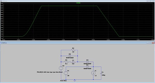
 Bild
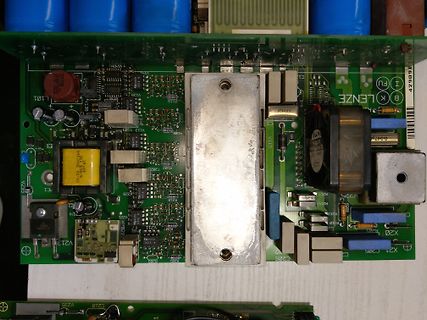
 Bild
 Bild
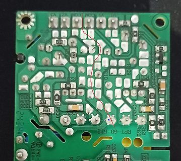
 Bild
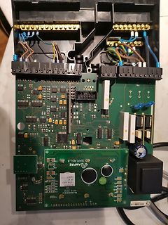
 Bild
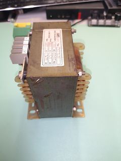
 Bild
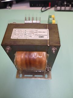
 Bild
 Bild
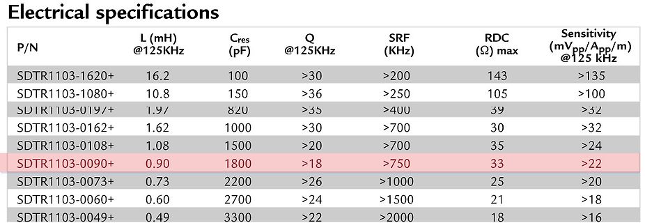
 Bild