-
Datei
main.c
**************************************************************** * Device Instance Opened on host side * ***************************************/ if (INTVAL & DEVICE_OPEN){ IE &= ~0x40; // SPI Interrupt ausschalten. P1 ^= 0x08; // Port 1 Pin 3 invertieren. (P0.1 am Knoten) asm("NOP");asm("NOP");asm("
in „Puffer-Problem mit C8051F320 (8051)“ · Mikrocontroller und Digitale Elektronik ·
-
Datei
CAN_RS232.asm
RXM0SIDL,ACCESS movwf RXM0EIDH,ACCESS movwf RXM0EIDL,ACCESS movwf RXF0SIDH,ACCESS ;Filter setzen (SID=0 EID=0) movlw 0x08 movwf RXF0SIDL,ACCESS movlw 0x00 movwf RXF0EIDH,ACCESS movwf RXF0EIDL,ACCESS movlw 0x60 movwf RXB0CON,ACCESS ;No Overflow to RXB1 ;set_Loopbackmode set_NormalMode movlw 0x10 ;0x50
in „PIC18F258 sendet kein CAN-Telegramm“ · Mikrocontroller und Digitale Elektronik ·
-
Datei
glcdneu.c
Enable_Pulse(); } void GLCD_Clrln(unsigned short ln) { int i; GOTO_XY(0,ln); //At start of line of left side GLCD_CS1low; GLCD_CS2high; for(i=0;i<65;i++) GLCD_Write(0); GOTO_XY(64,ln); //At start of line of right side GLCD_CS1high; GLCD_CS2low; for(i=0;i<65;i++) GLCD_Write(0); } void GLCD_CLR(void) { unsigned
in „Initialisierung eines GLCDs 128x64“ · Mikrocontroller und Digitale Elektronik ·
-
PDF
BI_82P_data.pdf
.10 (2) 2.54 Model 82W .21 5.3 .10 .18 2.5 4.57 Min. .020Min. (1) 0.51 (2) Standoffs (3) .10 2.5 SIDE ADJUSTMENT (Inch/mm) Model 82PA .36 .25 9.14 Min. .185 ± .015 6.35 .205 ± .015 4.669 ± 0.381 .012 5.207 ± 0.381 .17 Min. Housing: Metal .10 4.32 0.305 Case: Plastic 2.54 (3) .28 (2) 7.11 (1) .10 2.54
-
PDF
SST5912_Datasheet_Rev_A.pdf
Voltage VGD -25 V Gate-Source Voltage VGS -25 V Forward Gate Current G 50 mA Power Dissipation (per side) P D 300 mW (total) 500 mW o Power Derating (per side) 2.4 mW/ C (total) 4 mW/ C Operating Junction Temperature TJ -55 to 150 oC o Storage Temperature Tstg -65 to 150 oC Lead Temperature (1/16" from
in „Was ist das für ein Bauteil? Bzw welcher Hersteller?“ · Mikrocontroller und Digitale Elektronik ·
-
PDF
PT65.pdf
Hexadecimal accessories complement SCREWDRIVER SPINDLE SEGMENT WHEEL ACCESSORIES Upper actuation Side actuation Upper actuation Upper actuation Side actuation Upper actuation PT65101L254 BCD PT65101 PT65101L508 PT65301 PT65501 - PT65701 BCD COMPLEMENT PT65102 - - PT65502 - - HEXADECIMAL PT65103 PT65103L254
in „[V] Codierschalter 0-9 zu BCD, Printmontage (NOS)“ · Markt ·
-
PDF
BGA_Breakouts_and_Routing.pdf
pad. Disadvantages (Over Via-in-Pad) • If you have a ground or power plane on the BGA mount side, the fanout via pads prevent a continuous plane fill under the BGA. 68 Chapter Four – Fanout Patterns Figure 4-6: Quadrant dog-bone pattern 69 BGA Breakouts and Routing Figure 4-7: Quadrant dog-bone
-
PDF
Compaq_Portable_Plus_286_-_Maintenance_and_Service_Guide.pdf
CAUTION In the COMPAQ PORTABLE 286 Personal Computer, the mounting screw on the fixed disk drive side is longer than the other two mounting screws. To avoid damaging the diskette drives, replace the longer screw in its original location. >>>>>>>>>>>>>>>>>>>>>>>>>>>>>>>>>>>>>>><<<<<<<<<<<<<<<<<<<<<<<
-
PDF
MC34064.pdf
MC34063A, MC33063A 5.45 2.500 (Top view, copper foil as seen through the board from the component side) MC34063A MC34063A MC34063A (Top View, Component Side) *Optional Filter. Figure 13. Printed Circuit Board and Component Layout (Circuits of Figures 7, 9, 11) INDUCTOR DATA Converter Inductance ( H)
in „Negative Spannung in positive invertieren“ · Mikrocontroller und Digitale Elektronik ·
-
PDF
DS90LV047A.pdf
allows for be between 90Ω and 130Ω. Remember that the current easy PCB layout. The LVDS signals on one side of the mode outputs need the termination resistor to generate the device easily allows for matching electrical lengths of the differential voltage. LVDS will not work without resistor ter- differential
in „TFT Display 8bit 16bit 8080 Interface über LVDS“ · Mikrocontroller und Digitale Elektronik ·
-
PDF
DS90LV048A.pdf
mination. Typically, connecting a single resistor across the easy PCB layout. The LVDS signals on one side of the device easily allows for matching electrical lengths of the pair at the receiver end will suffice. differential pair trace lines between the driver and the re- Surface mount 1% to 2% resistors
in „TFT Display 8bit 16bit 8080 Interface über LVDS“ · Mikrocontroller und Digitale Elektronik ·
-
PDF
LM1086.pdf
to the output with input instantaneously shorted to ground, the regulator terminal on the positive side and directly tied to the ground could be damaged. In this case, an external diode is recom- terminal on the negative side. mended between the output and input pins to protect the regulator, shown in
in „Spannungsregler“ · Analoge Elektronik und Schaltungstechnik ·
-
PDF
DS90LV047A.pdf
allows for be between 90Ω and 130Ω. Remember that the current easy PCB layout. The LVDS signals on one side of the mode outputs need the termination resistor to generate the device easily allows for matching electrical lengths of the differential voltage. LVDS will not work without resistor ter- differential
in „Analogsignal über Twisted-Wire übertragen“ · Analoge Elektronik und Schaltungstechnik ·
-
PDF
DS90LV048A.pdf
mination. Typically, connecting a single resistor across the easy PCB layout. The LVDS signals on one side of the device easily allows for matching electrical lengths of the pair at the receiver end will suffice. differential pair trace lines between the driver and the re- Surface mount 1% to 2% resistors
in „Analogsignal über Twisted-Wire übertragen“ · Analoge Elektronik und Schaltungstechnik ·
-
PDF
doc8012.pdf
motors. Schematics are available from www.atmel.com. The switches connected to V ame called high side switches. The switches connected to ground are similarly called low side switches. When operating a BLDC motor as shown in Figure 1, only one high side and one low side switch is open at any time, creating
in „BLDC Regler nach AVR444 - brauche Hilfe“ · Mikrocontroller und Digitale Elektronik ·
-
PDF
142c38eef4c5eb392531e1bacd4aee1b.pdf
front of lead terminals A a≤ t, b≤1/5W, c≤3mm Max.3 15 defect defects crack allowed b B Crack at two sides of lead terminals should not cover patterns and alignment mark c w a t - 24 - Model No.:TM028HDZ30 V1.0 ②Surrounding crack―non-contact side seal t c b a b < Inner borderline of the seal Inner border line of the seal Outer border line of the seal ③ Surrounding crack― contact side seal t c b a b < Outer borderline of the seal Inner border line of the seal Outer border line of the seal ④Corner A a ≦ t, b ≦ 3.0, c ≦ 3.0 B Glass crack should not cover patterns u and alignment mark
in „Raspberry Pi Rev A TFT Display?“ · Digitale Signalverarbeitung / DSP / Machine Learning ·
-
PDF
WX_Station.pdf
1 2 3 4 5 6 A A Power supply MCU and peripherals User Interface High side switches 36V0 36V0 PWM0 PWM0 ENC_A ENC_A 36V0 36V0 IRON_0 IRON_0 24V0 PWM1 ENC_B 24V0 IRON_1 24V0 5V0 5V0 PWM1 ENC_B 24V0 IRON_1 12V0 12V0 3V3 PWM2 PWM2 ENC_SW ENC_SW 12V0 12V0 IRON_2 IRON_2 5V0 5V0
in „Weller WX/WSM/WHS Serie Kabel Reverse Engineering“ · Mikrocontroller und Digitale Elektronik ·
-
PDF
CAT24C164-D.PDF
2.54 BSC eB 7.87 10.92 PIN # 1 IDENTIFICATION L 2.92 3.30 3.80 D TOP VIEW E A2 A A1 c b2 L e b eB SIDE VIEW END VIEW Notes: (1) All dimensions are in millimeters. (2) Complies with JEDEC MS-001. http://onsemi.com 9 CAT24C164 PACKAGE DIMENSIONS SOIC 8, 150 mils CASE 751BD−01 ISSUE O SYMBOL MIN NOM MAX
in „Serielles EEprom 24C164“ · Mikrocontroller und Digitale Elektronik ·
-
PDF
ph320240t028-zea.pdf
width of crack. Z : The thickness of crack W : terminal length t : The thickness of glass a : LCD side length 8.1 General glass chip: 8.1.1 Chip on panel surface and crack between panels: Z X Y Y Z X 08 SP SP The crack of glass Minor Y 【 NG】 【 OK】 X Y Seal width Z X Y Z Crack can’t enter ≦ a viewing
in „SPI zu 8080 Parallel Wandler“ · Mikrocontroller und Digitale Elektronik ·
-
PDF
MC10EP31-D.PDF
DIMENSION A AND B DO NOT INCLUDE MOLD PROTRUSION. 8 5 4. MAXIMUM MOLD PROTRUSION 0.15 (0.006) PER SIDE. 5. DIMENSION D DOES NOT INCLUDE DAMBAR B S 0.25 (0.010) Y M PROTRUSION. ALLOWABLE DAMBAR 1 PROTRUSION SHALL BE 0.127 (0.005) TOTAL 4 IN EXCESS OF THE D DIMENSION AT K MAXIMUM MATERIAL CONDITION. −Y
in „Rechtecksignal mit Anstiegszeit < 1 ns für Oszi- und Tastkopf-Tests“ · HF, Funk und Felder ·
-
PDF
DDS.pdf
ਖ਼໘ Front view ଆ໘ Side view 10.0ʶ0.5 5.0ʶ0.5 19.5ʶ0.5 Χϥʔίʔυ ୈҰ৭ଳ First color band ୈೋ৭ଳ Second color band ୈࡾ৭ଳ Third color band Color code ܗ໊ Part number ϩοτ൪߸ͷ10ͷܻFirstdigitofproductLotNo. ϩοτ൪߸ͷ1ͷܻSeconddigitofproductLotNo
in „Hilfe Bauteilidentifizierung für Reparatur“ · Analoge Elektronik und Schaltungstechnik ·
-
 Bild
Bild
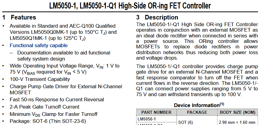
Datenblatt Ausschnitt LM5050-1 High-Side OR-ing FET Controller
LM5050-1, LM5050-1-Q1 High-Side OR-ing FET Controller 1 Features LM5050Q0MK-1, LM5050Q1MK-1 VIN: 1 V to 75 V 100-V Transient Capability N-Channel MOSFET 3 Description LM5050-1/-Q1 Device Information PART NUMBER: LM5050-1, PACKAGE:
in „Suche Protection IC“ · Analoge Elektronik und Schaltungstechnik · · Screenshots
-
Datei
Daten.c
********* * Function: * * Overview: * * * PreCondition: None * * Input: None * * Output: None * * Side Effects: ********************************************************************/ char Daten_Init(void){ unsigned int i=0; unsigned char buffer=0; unsigned int address=0; // Initialwert geben Anzeige_LokListe.FirstItem
in „Array beschreiben schlägt fehl“ · Mikrocontroller und Digitale Elektronik ·
-
PDF
2201pdf.pdf
alldatahavingbeengatheredatstandardtestconditions(see sensitivity characteristics for Element 2, all data having been reverse side of this sheet). The Y-axis is indicated as sensor gathered at standard test conditions (see reverse side of this resistance ratio (Rs/Ro) which is defined as follows: sheet). The Y-axis is indicated
in „Portablen Luftsensor bauen“ · Mikrocontroller und Digitale Elektronik ·
-
Datei
pap.txt
AIRmatic/data/settings.html#400-400), lines 400 to 575 Now I'll open Wireless.ino to see the server-side handling of the session, seeds, and encryption. Read [](file:///g%3A/src/vscode/AIRmatic/Wireless.ino#1-1), lines 1 to 400 Read [](file:///g%3A/src/vscode/AIRmatic/Wireless.ino#400-400), lines 400 to
in „Programmieren mit KI“ · Offtopic ·
-
Datei
test.c
LED_Ring_DATA_ON(); // Auswahl der LOD-Erkennungsspannung // Max 0b111 LED_Ring_clock(); } for(i=0;i<2;i++){ // SID load control 0b11 LED_Ring_DATA_ON(); // SID-Laststeuerung // OFF 0b11 LED_Ring_clock(); } // Helligkeit 0-127 //000 0000 bis 111 1111 for(i=0;i<7;i++){ // Global brightness control (BC) data for BLUE
in „includes in Cube IDE“ · Mikrocontroller und Digitale Elektronik ·
-
PDF
602W2CSXX74S20X.pdf
CONTACTS 30A: COPPER ALLOY ( D D PLATING MATING AREA: GOLD FLASH over NICKEL , PLATING TERMINATION SIDE: 160-240µin TIN over 80µin NICKEL 3 6,35 ` 0,3 Ø 6. THREADED INSERTS: COPPER ALLOY; min. 200µin TIN over 80µin NICKEL ( 5 : 1 ) 7. METAL BRACKETS: ZINC DIE CAST; 300µin COPPER , 0 / 40-120µin NICKEL
in „Leistungsstecker“ · Platinen ·
-
PDF
muArt_Schematics.pdf
1 2 3 4 ← HOST SIDE PERIPHERAL SIDE → A VDD VDD VIO A U1 1 VDDA VDDB 16 REVERSE POLARITY PROTECTION R14 R1 C1 C2 2 GNDA GNDB 15 C3 C4 R33 Q1 DMG2301LK 392 1K 100nF 100nF 100nF 100nF 1K L4 VIO 8 GNDA GNDB 9 VIO_CON D S
in „muArt - Der zuverlässige und universelle UART-Konverter“ · Mikrocontroller und Digitale Elektronik ·
-
PDF
weller_driver_v1_circuit_diagram__1_.pdf
controller, the ESD protection might or might not work. Connector pinouts above are seen from contact side, not solder side. D D http://kair.us/ 1 2 3 4 5 6
in „Weller WMRT-MS Micro-Pinzette Inside ?“ · Mechanik, Gehäuse, Werkzeug ·
-
PDF
1038_1_.pdf
Balanced RF SAW Filters Standard Ethernet cable plugs directly into the RJ45 connector on the network "side" of the Module. Serial "side" interfaces directly to the serial port pins of most compatible with GSM microcontrollers, microprocessors, UARTs, etc. networks from Murata From the hardware standpoint
in „[V] 2St alte unbenutzte TIBBO Netzwerkmodule EM202-00“ · Markt ·
-
PDF
DSAIH000309343.pdf
+ pin. CAP2+ O Pin connected to the positive side of the step-up capacitor. 6 Connect the capacitor between this pin and CAP2- pin. CAP2- O Pin connected to the negative side of the step-up capacitor. 6 Connect the capacitor between this pin and CAP2
in „Pollin Display VL-FS-COG-VLGEM1277-01“ · Mikrocontroller und Digitale Elektronik ·
-
PDF
Abdel-Rahman_Osama_A_200705_PhD.pdf
Buck converter; it is observed that the reverse-recovery related ringing is very severe and high-side switch S1 operates at hard switching. In order to test the QSW buck converter, the filter inductance value has been reduced from 27uH to 3uH, the high-side switch achieves ZVS as shown in Fig. 3.8(b
in „Welche Schaltfrequenz bei Step-Down EMV-günstig?“ · Analoge Elektronik und Schaltungstechnik ·
-
PDF
Panasonic_AG-7350-7150_Service_Manual.pdf
the Side Panels 2-2-4. Removal of the 34P C. B.A. 1. Unscrew the 8 screws (B) on the Side Panels 1. Unscrew the 4 screws (D) on the 34P C.B.A. (Figure D3). (Figure D5). 2. Lift the Side Panels. 2. Careful lift
in „Totalausfall Panasonic AG-7350 (nur noch Hintergrundbeleuchtung der Zeigerinstrumente)“ · Analoge Elektronik und Schaltungstechnik ·
-
PDF
Datenblatt_Epson_S1D15G10_vom_Display_Controller.pdf
List of Device Models.” Potential on board GND Bump size Tolerance: ±4 µm (reference) Driver output side: (SEG1 to 396) 41.5 µm (COM1 to 33, 101 to 132) 48µm (COM34 to 100) 45µm Driver input side: 82 µm × 109 µm Bump pitch Driver output side: 42 µm I/O signal line side:100 µm min. Bump height 22.5 µm±4
in „The Siemens S65 132x176, 65536 color display with AVR“ · Projekte & Code ·
-
PDF
S1D15G10.pdf
List of Device Models.” Potential on board GND Bump size Tolerance: ±4 µm (reference) Driver output side: (SEG1 to 396) 41.5 µm (COM1 to 33, 101 to 132) 48µm (COM34 to 100) 45µm Driver input side: 82 µm × 109 µm Bump pitch Driver output side: 42 µm I/O signal line side:100 µm min. Bump height 22.5 µm±4
-
PDF
TC35_datasheet.pdf
Shielding cover baseband Shielding frame baseband PCB including ZIF connector and antenna TC35 baseband side TC35 RF side connector Shielding frame RF Shielding cover RF TC37 baseband side TC37 RF side Figure 24: Exploded diagram and PCBs of TC35/TC37 TC35_37_HD_02_V03.10 - Released Page 59 of 92 21.12.2001
in „Schaltplan TC35-Modul?“ · Mikrocontroller und Digitale Elektronik ·
-
PDF
R-IN32M-CL_CC-Link_IE_Field_Intelligent_device_station.pdf
undershooting? PHY- RJ45 connctor The signal lines between PHY and RJ45 connector mus be connected in + 2 side and + side of each terminal, - side and – side of each terminal. connection Otherwise 1000BASE-T compliance test fails. Are pull-up resistors installed for the data signals D15 to D00? (10-kΩ 3 Data
in „Wie funktioniert der Interrupt- bzw. Eventaufruf?“ · Mikrocontroller und Digitale Elektronik ·
-
PDF
AVR223_Digital_Filters_with_AVR.pdf
ranges of the summations M and N are referred to as the filter order or the filter length. The right side of the equation describes the feedforward in the filter function and the left side the feedback in the filter function. A filter function can consist of either or both sides of the differential equation. If only the right side of the differential equation is used, the filter is a FIR filter (N 0 and M = 0). If both sides are used the filter is an IIR filter (N ≠ 0 and M ≠ 0). A special case is when only the left side of the
in „Koeffizienten von DGL berechnen“ · Digitale Signalverarbeitung / DSP / Machine Learning ·
-
PDF
24LC256_32k_I2C-EEPROM.pdf
include mold flash or protrusions. Mold flash or protrusions shall not exceed .010” (0.254mm) per side. JEDEC Equivalent: MS-001 Drawing No. C04-018 DS21203M-page 14 2004 Microchip Technology Inc. 24AA256/24LC256/24FC256 8-Lead Plastic Small Outline (SN) – Narrow, 150 mil (SOIC) E E1 p D 2 B n 1 h
in „immer noch EEprom“ · Mikrocontroller und Digitale Elektronik ·
-
PDF
datasheetMax3392.pdf
the CC side of the VL ≤ VCC ≤ +3.3V) 2 device, and vice-versa. The MAX3374E/MAX3375E/ Bidirectional Level Translation E MAX3376E/MAX3379E and MAX3390E–MAX3393E unidi- (MAX3372E/MAX3373E and rectional level translators
in „Max3392 Pegelwandler, BlueNiceCom 4“ · Mikrocontroller und Digitale Elektronik ·
-
PDF
AN10897.pdf
spacing (mm) Fig 24. Inductance as a function of ground grid spacing Ideally, the top and bottom side of the PCB should look like a ground plane with horizontal ground traces on one side, and vertical ground traces on the other side. It is not absolutely necessary that the traces be orthogonal. The
in „50 X LM75 an ATMEGA16?“ · Mikrocontroller und Digitale Elektronik ·
-
PDF
esp8266_hardware_design_guidelines_en.pdf
1-9) and chip enable pin CH_EN (2-1-10), respectively. When the switches are toggled to the outer side, the voltage level is high, while when the switches are toggled to the inner side, the voltage level is low. • For the 5V power switch: - Toggled to the inner side, the board is powered on; Slide switch - Toggled to the outer side, the board is powered off. • For the GPIO0 Control: - Toggle to the inner side, the UART download mode is enabled and users can download firmware with ESP Flash Download Tool; - Toggle to the outer side
in „MCP1700-3302 mit ESP8266“ · Mikrocontroller und Digitale Elektronik ·
-
PDF
EMV_Design.pdf
spacing (mm) Fig 24. Inductance as a function of ground grid spacing Ideally, the top and bottom side of the PCB should look like a ground plane with horizontal ground traces on one side, and vertical ground traces on the other side. It is not absolutely necessary that the traces be orthogonal. The
-
PDF
A4964_AN_R2.pdf
bridge, a dead time isrequiredbetweengenerating a calculatedusing the followingequation: loworhigh side turn offsignal and a complementaryturnon 𝑉𝐼𝐿𝐼𝑀 = 𝑉 𝑀𝐼𝑇 × 𝑉 𝐼𝑆𝐶 signal. The duration ofthe dead time can be selectedusingthe “Dead Time” option. Where V MITisthe maximum thresholdofthe sense
in „Allegro A4964 Demoboard - ein Phantom?“ · Analoge Elektronik und Schaltungstechnik ·
-
PDF
INF-8074i.pdf
0.1 Transceiver height, rear D 13.4 ± 0.1 Transceiver width, rear E 1.0 Maximum Extension of front sides outside of cage, see Note 2 Figure 1B F 2.3 Reference Location of cage grounding springs from centerline, top G 4.2 Reference Location of side cage grounding springs from top H 2.0 Maximum Width of
in „SFP - Single Fibre Port Chip Ansteuerung“ · Mikrocontroller und Digitale Elektronik ·
-
PDF
Transient_Simulation.pdf
referencevalue: 755.3 A, peak value; ferential current id=iaZ-ial of the most stressed 370MVA, 400kV, HV side): phase ip per unit; reference current of H.V.side: 755.3 A, peak value. Flux linkages with the coils: density is assumed to be equal to 1.7 T; therefore 0.707.1.7/0.57=2.11 T). 0.91% 3% In the parallel
in „ltspice kopelfaktoranweisung für Drehstromtrafo“ · Analoge Elektronik und Schaltungstechnik ·
-
PDF
hc86.pdf
DIMENSIONS A AND B DO NOT INCLUDE MOLD PROTRUSION. 14 8 4. MAXIMUM MOLD PROTRUSION 0.15 (0.006) PER SIDE. –B– 5. DIMENSION D DOES NOT INCLUDE DAMBAR P 7 PL 0.25 (0.010) M B M PROTRUSION. ALLOWABLE DAMBAR 1 7 PROTRUSION SHALL BE 0.127 (0.005) TOTAL IN EXCESS OF THE D DIMENSION AT MAXIMUM MATERIAL CONDITION
in „Vollbrücke, wo kondensatoren einbauen?“ · Analoge Elektronik und Schaltungstechnik ·
-
PDF
Kompassmodul.pdf
Sensor 1 Sensor 2 8 RX HOST LCD 2XCM-I T2 5 T 6 7 TX 1 9 GND Package drawing : a N N E . c b Front Side 12 Version 2.0 KAOT-DAR g d e h f Left Side a c b Bottom Side Millimeters Inches (10 ) Symbol mm Mil a 19.8 780 b 28.5 1122 c 2.6 102 d 0.6 24 e 2.6 102 f 8.8 347 g 2.8 110 h 12.2 480 13 Version 2.0
in „Wer rettet meine Facharbeit - UART Problem TXC bit“ · Mikrocontroller und Digitale Elektronik ·
-
Datei
vga.vhd
std_logic; busy : out std_logic; -- SRAM side SRAM_ADDR : out std_logic_vector(17 downto 0); SRAM_CE_N : out std_logic; SRAM_DQ : inout std_logic_vector(15 downto 0); SRAM_LB_N : out std_logic; SRAM_OE_N : out std_logic; SRAM_UB_N : out std_logic; SRAM_WE_N : out std_logic; -- VGA side CLOCK_25 : in std_logic; VGA_BLANK : out std_logic; VGA_B : out std_logic_vector(9 downto 0); VGA_CLK : out std_logic; VGA_G : out std_logic_vector(9 downto 0); VGA_HS : out std_logic; VGA_R : out std_logic_vector
-
PDF
Kompassmodul.pdf
Sensor 1 Sensor 2 8 RX HOST LCD 2XCM-I T2 5 T 6 7 TX 1 9 GND Package drawing : a N N E . c b Front Side 12 Version 2.0 KAOT-DAR g d e h f Left Side a c b Bottom Side Millimeters Inches (10 ) Symbol mm Mil a 19.8 780 b 28.5 1122 c 2.6 102 d 0.6 24 e 2.6 102 f 8.8 347 g 2.8 110 h 12.2 480 13 Version 2.0
in „Problem mit Mega128 USART“ · Mikrocontroller und Digitale Elektronik ·