surface mount The ratiomatric solution was used with a calibrated PT100 RTD with 0.2°C/mW self-heat coefficient would RTD simulator [4] to generate the data as shown in dissipate 0.002°C with 300 µA bias current at 0°C Table 1. The graph in Figure 1 shows that the ratiomet- (100Ω), and
ADE-1 Level 7 (LO Power +7 dBm) 0.5 to 500 MHz Maximum Ratings Features Operating Temperature -40°C to 85°C • low conversion loss, 5.0 dB typ. CASE STYLE: CD636 • excellent L-R isolation, 55 dB typ. Storage Temperature -55°C to 100°C PRICE: $2.49 ea. QTY (20) RF Power 50mW • excellent IP3, 15 dBm typ
ADE-1 Level 7 (LO Power +7 dBm) 0.5 to 500 MHz Maximum Ratings Features Operating Temperature -40°C to 85°C • low conversion loss, 5.0 dB typ. CASE STYLE: CD636 • excellent L-R isolation, 55 dB typ. Storage Temperature -55°C to 100°C PRICE: $2.49 ea. QTY (20) RF Power 50mW • excellent IP3, 15 dBm typ
SD Karten Modul in ein Systemtelefon integrieren. Im Systeltelefon wird ein 8051 Modell verwendet (AT89C51RB2). Hier wird mit dem Keil C51 Compiler gearbeitet. Ich möchte nun gerne die beiden Informationsregister CID und CSD der SD Karte auslesen. Diese sind jeweils 16 (+ 2 Byte CRC) Byte lang. Beide
Du hast recht, ist ja ein 8Bitter, also kein pragma pack. Habe dein Bsp. mal umgebaut [c] #pragma CODE #include <REG52.H> #include <string.h> typedef unsigned char t_uchar; typedef unsigned int t_uint; const t_uchar ser[] = { 0x03, 0x53, 0x44, 0x53, 0x44, 0x30, 0x32, 0x47
w:0xff:m -Ulfuse:w:0xc2:m avrdude: Version 5.11, compiled on Sep 2 2011 at 18:52:52 Copyright (c) 2000-2005 Brian Dean, http://www.bdmicro.com/ Copyright (c) 2007-2009 Joerg Wunsch System wide configuration file is "/Applications/Arduino-1.app
sollte sowas wie STK500 raus kommen?! * starte den Programmiervorgang mal ohne angeschlossenen µC * Prüf mal die Verkablung zwischen STK500(alias Arduino) und deinem µC. Die Kommunikation die AVRDude im Log anzeigt ist nicht die zwischen µC und Programmer sondern die zwischen AVRDude und Programmer
SELECT 0xA1 Inverse scan (L to R) 0xA0 Normal Scan R to L 0xA1 Inverse Scan L to R COMMON DIRECTION 0xC0 Scan commons top to bottom SELECT 0xC0 Normal scan top to bottom 0xC8 Inverse scan bottom to top INITIAL DISPLAY LINE 0x40 Start COM scan at line address 00H SET 0x7F start COM scan at line 3FH Use
are shown in millimeters (inches) DIMENSIONS 6 A 5 MILLIMETERS INCHES D SYMBOL MIN MAX MIN MAX A 0.89 1.12 A A2 C A1 0.01 0.10 0.0004 3 E A2 0.88 1.02 6 E1 0.15[0.006] M C B A b 0.30 0.50 1 2 0.10 [0.004] C c 0.08 0.20 A1 3X b D 2.80 3.04 e 5 B 0.20 [0.008] M C B A E 2.10 2.64 e1 NOTES: E1 1.20 1.40
are shown in millimeters (inches) DIMENSIONS 6 A 5 MILLIMETERS INCHES D SYMBOL MIN MAX MIN MAX A 0.89 1.12 A A2 C A1 0.01 0.10 0.0004 3 E A2 0.88 1.02 6 E1 0.15[0.006] M C B A b 0.30 0.50 1 2 0.10 [0.004] C c 0.08 0.20 A1 3X b D 2.80 3.04 e 5 B 0.20 [0.008] M C B A E 2.10 2.64 e1 NOTES: E1 1.20 1.40
C823 baudrate 898A Bandbreite C0C1 RX on CE89 FIFO CE8B enable FIFO Statusregister und FIFO auslesen: SEL=1 ; Grundzustand der Selekt-Leitung SDI=0 ; Datenleitung auf Lo nSEL
Hi an alle RFM12 Nutzer, ich habe den Treiber erfolgreich auf den PIC für den CCS C Compiler und den Microchip C18 Compiler portiert. Alle Infos dazu habe ich hier zusammengefasst: http://members.aon.at/electronics/pic/projects/rfm12/rfm12.html MfG
. Colour of Illumination Blue-Green(Filter for colours) Operating Temperature -40°C to +85°C Storage Temperature -40°C to +85°C Operating Humidity (non condensing) 20 to 80% RH @ 25°C SOFTWARE COMMANDS IDC DATA CONNECTOR PCB JUMPERS (O)PEN (L)INK Instruction D0-D7 Instruction D0-D7
demultiplexer b bit number i of the cell identifier i cm,l,k complex cell for frame m in OFDM symbol l at carrier k C' Complex modulation for a reference signal at carrier k k C'l k Complex modulation for a TPS signal at carrier k in symbol l C/N Carrier-to-Noise ratio Δ time duration of the guard interval
temperature prior to use. To warm the refrigerated paste, let the unopened container stand for 4 hours at ambient temperature before use. For faster warm up, place the sealed container in a water bath at ambient temperature for 30 minutes. Unopened Container 2–10 °C [35–50 °F] 6 months from date of manufacture
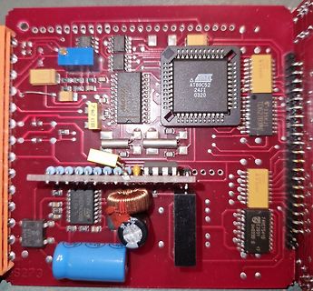
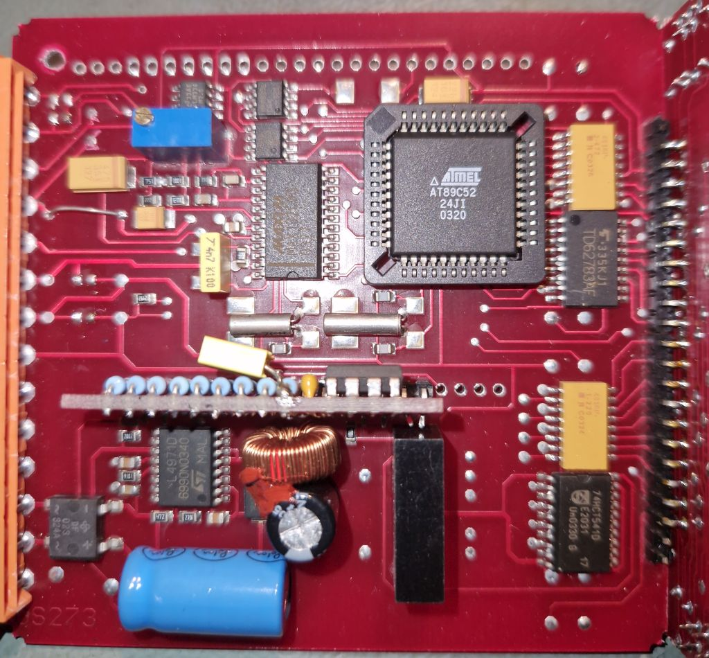
@nepomuk Es ist ein AT89S52 auf der Hauptplatine @wolf17 Wieso mechanisch? 2 Motoren werden mit EINEM Positioner aktuell gesteueert. Es soll ein zweiter Positioner zum ersten synchron laufen. Dabei müssten beide Geräte
dem Leser viel Sucherei ersparen, also z.B. Robert F. schrieb im Beitrag #7995359: > Es ist ein AT89S52 auf der Hauptplatine Robert F. schrieb im Beitrag #7995359: Und bitte bring es auf den Punkt. Wenn du in einem längeren Beitrag auf sieben Leute eingehst, wäre es deutlich übersichtlicher,
–04/06 Using the AT90USBKey 2.3 Reset Although the AT90USB has its on-chip RESET circuitry (c.f. AT90USB Datasheet, section “System Control and Reset), the AVRUSBKey provides to the AT90USB a RESET signal witch can come
Figure 51, the output error voltage is application circuits with high sensitivity. approximately 100 μV at room temperature, increasing to about C F 1 mV at 85°C. 10pF The maximum achievable signal bandwidth is RF 10MΩ ft fMAX = 2πR F F PHOTODIODE VOS where f tis the unity gain frequency of the amplifier.
110 dB SupplyVoltage Range ±5 ±16.5 ±5 ±16.5 ±5 ±16.5 V Supply Current 4 5 4 5 4 5 mA OUTPUTVOLTAGE, AT R L 2 kΩ TMINtoTMAX ±10 ±10 ±10 V Output Short-Circuit Current 25 25 25 mA TEMPERATURE RANGES N Package 0 70 0 70 °C D Package −25 +85 −25 +85 −55 +125 °C 1 2Ifone terminal ofeach differential channel
das BIOS-Update ausführen will meldet mir Tenberry's DOS/4G - Extender folgende Fehlermeldung: [c]DOS/4G error (2001) exception 06h (invalid opcode) at 1A0:0016B600[/c] Dann folgt noch eine Tabelle mit irgendwelchen Speicheraddressen/Registern etc. von denen ich absolut keine Ahnung habe was sie
Karte bei etwa 62 Grad, >CPU 54 Grad - also normal. Watt? Nix da, CPU darf bei Volllast(!!!) 40°C nicht übersteigen, die GPU maximal(!) 50°C.
the aid of Fig.6 we find the maximum value of S and the normalized values of the correction elements C 1n and L1n C 1n L 1n× R 1 Now C a1d L ca1 be calculated: C1 = - and L 1 - ω max × R1 ω max 1998 Mar 23 5 Philips Semiconductors Design of H.F. Wideband Power Transformers; Part II ECO7213 At the secondary
in the correct order followed by the address. Example; to change the address of a sonar currently at 0xE0 (the default shipped address) to 0xF2, write the following to address 0xE0; (0xA0, 0xAA, 0xA5, 0xF2 ). These commands must be sent in the correct sequence to change the I2C address, additionally
switching the input signal for "black" and "white" . White Black White u 100% t e 90% u l O a o V c i e at d e t R( 10% h 0% P τ r τ d Time 【Note4】This shall be measured at center of the screen. 【Note5】Definition of white uniformity: H 1/4H 1/4H 1/4H 1/4H 1 Maximun Luminance of 5 points V δw = A D
AGND –0.3 AVDD + 0.3 V V Parameter is a typical value only. ENVIRONMENTAL 1 VI 100% production tested at 25°C; guaranteed by de- Operating Temperature –40 +85 °C sign and characterization testing for industrial tem- Junction Temperature 150 °C perature range; 100% production tested at tempera- Lead Temperature
ZAD-11+ Level 7 (LO Power +7 dBm) 5 to 2000 MHz Maximum Ratings Features Operating Temperature -55°C to 100°C • low conversion loss, 7.12 dB typ. CASE STYLE: M22 Storage Temperature -55°C to 100°C • wideband, 5 to 2000 MHz Connectors Model Price Qty. RF Power 50mW • rugged shielded case BNC ZAD-11+
C AA18 PB49B 4 C W16 PB50A 4 T W16 PB50A 4 T U15 PB50B 4 C U15 PB50B 4 C V16 PB51A 4 T V16 PB51A 4 T U16 PB51B 4 C U16 PB51B 4 C Y17 PB52A 4 T Y17 PB52A 4 T V17 PB52B 4 C V17 PB52B 4 C AB20 PB53A 4 T AB20
C AA18 PB49B 4 C W16 PB50A 4 T W16 PB50A 4 T U15 PB50B 4 C U15 PB50B 4 C V16 PB51A 4 T V16 PB51A 4 T U16 PB51B 4 C U16 PB51B 4 C Y17 PB52A 4 T Y17 PB52A 4 T V17 PB52B 4 C V17 PB52B 4 C AB20 PB53A 4 T AB20
S11 S 12 D1 S S S S P1.2 P0.2 13 14 15 16 D 2 P1.3 P0.3 Figure 1 D 3 P1.4 P1.5 P1.6 P1.7 INTO P3.2 C1 IC1 2.2 F MCS-51 FAMILY MICROCONTROLLER (AT89C52) NOTE: DIODES ARE IN4148. Adding an interrupt-driven keypad to an MCS-51 family microcontroller requires only a few components.
Phase C voltage input should be wired to the VBP pin. The nominal reference voltage at the REF IN/OUTpin is 2.42 V. This is the reference voltage used for the ADCs in the ADE7758. However, the current channels
shown in Figure 35a & 35b. The Write Status Register instruction (01h) and Erase instructions (20h, 52h, D8h, C7h, 60h, 44h) are not allowed during Erase Suspend. Erase Suspend is valid only during the Sector or Block erase operation. If written during the Chip Erase operation, the Erase Suspend instruction
mW Standby Mode 25 42 mW Shutdown Mode 10 31.5 µW 1Temperature range for the B versionis−40°Cto+85°C. TheAD7606 isoperational up to 125°C with throughput rates≤ 160 kSPS, and the SNR typically reduces by 0.7 dB at 125°C. 2See the Terminology section. 3Thisspecificationapplieswhenreadingduringaconversionorafteraconversion.IfreadingduringaconversioniDRIVEV
connected. Integrated Silicon Solution, Inc.- www.issi.com 9 Rev. L9 02/20/2022 IS25LP128 3. BLOCK DIAGRAM C o tolLogi HighV olageG enertor Sttus IO Bufersand Registr D at Lathes C E# 256B yes Page Bufer e SC K c r t W P# l (O2) r Y - ec der h SI r (O0) e l SO r (O1) S (1) HO LD# orRES ET# r (IO3) d o e M emoryArray
first data byte addressed is shifted out on the IO1 and IO0 lines, with each pair of bits shifted out at a maximum frequencyfC, during the falling edge of SCK. The first bit (MSB) is output on IO1, while simultaneouslythe second bit is output on IO0. The first byte addressed can be at any memory location
off. A B V PK C TON T PER FIGURE 38. TIMING DIAGRAM FOR HALF-BRIDGE CONVERTER It can be seen that the voltage pulses on the transformer secondary side (applied to the L-C filter) are occurring at twice the frequency
Unter C0126x gibts in meiner icao24plus.txt keine Skyhawks. Meinst du diese: C01295 C-FHAY C172 Cessna 172 Skyhawk/Cutlass C012C0 C-FHCP C172 Cessna 172 Skyhawk/Cutlass ? Wenn ich deren icao24 als
Hallo Michael, nein ich meinte folgende Maschinen: C01266 C-FGZD A4 McDonnell Douglas A-4N C01267 C-FGZE A4 McDonnell Douglas A-4N C0126A C-FGZH A4 McDonnell Douglas A-4N C0126B C-FGZI A4 McDonnell Douglas A-4N C01271 C-FGZO A4 McDonnell
H) 70.7 X 38.8 mm Number of dots 128 X 64 dots Dots size(W x H) 0.48 X 0.48 mm Dots pitch(W x H) 0.52 X 0.52 mm 1.2. BLOCK DIAGRAM 3 WWW.TINSHARP.COM TG12864B-03 1.3 MECHANICALSPECIFICATION E . E T D B D T M . N O L P C I R S E A C S H N : S O N T T I R D A N T T D T D C N 性 / L O 特 C E C 组 G 模 N 改 L
m l n n r u m n b o o W m C t h C C h s o f s f o C o S S l o H i P P P y i i Z Z Z R i S T E Z Z W T N D A A D A A C D D C D D Figure 29. Timing Diagrams at Data Write The stop transmission command may occur when the card is in

 Bild
Bild