-
Datei
version_1p3_assembler.asm
;ERROR TYPE ERRNUM: DS 2 ;WHERE TO GO ON AN ERROR VARTOP: DS 2 ;TOP OF VARIABLE STORAGE ST_ALL: DS 2 ;STORAGE ALLOCATION MT_ALL: DS 2 ;MATRIX ALLOCATION MEMTOP: DS 2 ;TOP OF MEMORY RCELL: DS 2 ;RANDOM NUMBER CELL DS FPSIZ-1 CXTAL: DS 1 ;CRYSTAL DS FPSIZ-1 FPT1: DS 1 ;FLOATINP POINT TEMP 1 DS FPSIZ-1 FPT2: DS 1 ;FLOATING POINT TEMP 2 INTLOC: DS 2 ;LOCATION TO GO TO ON INTERRUPT STR_AL: DS 2 ;STRING ALLOCATION SPV: DS 2 ;SERIAL PORT
in „Spaß mit Kloeckner-Moeller PS3 in BASIC(?)“ · Projekte & Code ·
-
Datei
version_1p3_assembler.asm
ERRNUM: DS 2 ;WHERE TO GO ON AN ERROR VARTOP: DS 2 ;TOP OF VARIABLE STORAGE ST_ALL: DS 2 ;STORAGE ALLOCATION MT_ALL: DS 2 ;MATRIX ALLOCATION MEMTOP: DS 2 ;TOP OF MEMORY RCELL: DS 2 ;RANDOM NUMBER CELL DS FPSIZ-1 CXTAL: DS 1 ;CRYSTAL DS FPSIZ-1 FPT1: DS 1 ;FLOATINP POINT TEMP 1 DS FPSIZ-1 FPT2: DS 1 ;FLOATING POINT TEMP 2 INTLOC: DS 2 ;LOCATION TO GO TO ON INTERRUPT STR_AL: DS 2 ;STRING ALLOCATION SPV: DS 2 ;SERIAL PORT
in „Basic für 80C31“ · Mikrocontroller und Digitale Elektronik ·
-
Datei
IS52Basic.a51
ERRNUM: DS 2 ;WHERE TO GO ON AN ERROR VARTOP: DS 2 ;TOP OF VARIABLE STORAGE ST_ALL: DS 2 ;STORAGE ALLOCATION MT_ALL: DS 2 ;MATRIX ALLOCATION MEMTOP: DS 2 ;TOP OF MEMORY RCELL: DS 2 ;RANDOM NUMBER CELL DS FPSIZ-1 CXTAL: DS 1 ;CRYSTAL DS FPSIZ-1 FPT1: DS 1 ;FLOATINP POINT TEMP 1 DS FPSIZ-1 FPT2: DS 1 ;FLOATING POINT TEMP 2 INTLOC: DS 2 ;LOCATION TO GO TO ON INTERRUPT STR_AL: DS 2 ;STRING ALLOCATION SPV: DS 2 ;SERIAL PORT
in „Layout für MCS51 Experimentierboard“ · Projekte & Code ·
-
Datei
IS52Basic.a51
ERRNUM: DS 2 ;WHERE TO GO ON AN ERROR VARTOP: DS 2 ;TOP OF VARIABLE STORAGE ST_ALL: DS 2 ;STORAGE ALLOCATION MT_ALL: DS 2 ;MATRIX ALLOCATION MEMTOP: DS 2 ;TOP OF MEMORY RCELL: DS 2 ;RANDOM NUMBER CELL DS FPSIZ-1 CXTAL: DS 1 ;CRYSTAL DS FPSIZ-1 FPT1: DS 1 ;FLOATINP POINT TEMP 1 DS FPSIZ-1 FPT2: DS 1 ;FLOATING POINT TEMP 2 INTLOC: DS 2 ;LOCATION TO GO TO ON INTERRUPT STR_AL: DS 2 ;STRING ALLOCATION SPV: DS 2 ;SERIAL PORT
in „Basic für 80C31“ · Mikrocontroller und Digitale Elektronik ·
-
 Bild
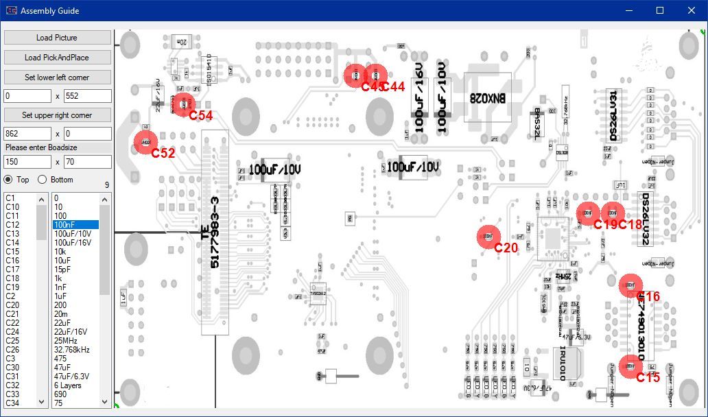
CAD-Ansicht eines Leiterplatten-Layouts mit Bestückungsdaten
x 0 Please enter Boardsize 150 x 70 Top Bottom 9 C1 0 C10 10 C11 100 C12 100uF/10V C13 100uF/10V C14 100uF/16V C15 16 C16 10uF C17 15pF C18 1k C19 1mF C20 200 C21 20m C22 22uF C24 22uF/16V C25 25MHz C26 32.768kHz C3 475 C30 47uF C31 47uF/6.3V C32 6 Layers C33 690 C34 75 C52 C54 C44 C19 C18 C20 C16 C15 100uF/10V 100uF/10V 8X02N DS26LU32 DS26LU32
in „Altium Designer - Assistent zur manuellen Bauteilbestückung“ · Platinen · · Layouts
-
PDF
OPTREX_F-51320AE_TechSpec.pdf
READ CCLR 70 - ns Control High Pulse Width WRITE tCCHW 30 - ns READ tCCHR 30 - ns Data Setup Time tDS8 30 - ns Data Hold Time tDH8 10 - ns t RD Access Time ACC8 - 70 ns Output Disable Time tOH8 5 50 ns V DD=2.7~4.5V Parameter Symbol Min. Max. Units Address Setup Time tAW8 0 - ns Address Hold Time tAH8
in „Pollin Grafik LCD-Modul OPTREX F-51320AE“ · Mikrocontroller und Digitale Elektronik ·
-
Datei
BCS33.ASM
-10 ; INT TLEN: equ TEND-11 ; LEN TPEEK: equ TEND-12 ; PEEK TRND: equ TEND-13 ; RND TUSR: equ TEND-14 ; USR ;------------------------------------------------------------------------------ ; Arbeitsspeicher ;------------------------------------------------------------------------------ org RAM PBEG: ds
in „Z80 SBC Problem.“ · Mikrocontroller und Digitale Elektronik ·
-
PDF
CD4007.pdf
immunity0.45 CC (typ.) P a r Ordering Code: P u Order Number Package Number Package Description s CD4007CM M14A 14-Lead Small Outline Integrated Circuit (SOIC), JEDEC MS-120, 0.150” Narrow e CD4007CN N14A 14-Lead Plastic Dual-In-Line Package (PDIP), JEDEC MS–001, 0.300” Wider Devices also available in Tape and
in „Fragen zum Transmission-Gate (Messergebnis)“ · Analoge Elektronik und Schaltungstechnik ·
-
PDF
FAN7621-36163.pdf
14 LO 0.4/ 0.6 V Delay Delay Gate Drive + 350ns + OLP S Q Shutdown without delay 5 V - LV + LVCCgood R -Q + -1 CC Auto-restart Q S 50ns Delay 23 V - Protection - 0.9 V OVP -Q R VAOCP Latch TSD 16 PG Protection
in „Verbindung einer Leuchtdiode mit einem Fototransistor erzeugen“ · Analoge Elektronik und Schaltungstechnik ·
-
PDF
DEM240128BFYH-LY.PDF
2002/04/03 2 ADDING VERSION 2003/01/10 CHANGE BLOCK DIAGRAM, PIN 3 ASSIGNMENTAND ELECTRICAL 2004/01/14 CHARACTERISTICS PREPARED BY: HZJ DATE: 14/01/2004 APPROVED BY: MH DATE: 20/01/2004 DEM240128B FYH-LY Product Specification CONTENTS 1. FUNCTIONS & FEATURES--------------------------------------------
in „glcd DEM240128B mit S6B2086X1 Controller (240x128px), wie ansteuern?“ · Mikrocontroller und Digitale Elektronik ·
-
Datei
IS51Basic.ASM
ERRNUM: DS 2 ;WHERE TO GO ON AN ERROR VARTOP: DS 2 ;TOP OF VARIABLE STORAGE ST_ALL: DS 2 ;STORAGE ALLOCATION MT_ALL: DS 2 ;MATRIX ALLOCATION MEMTOP: DS 2 ;TOP OF MEMORY RCELL: DS 2 ;RANDOM NUMBER CELL DS FPSIZ-1 CXTAL: DS 1 ;CRYSTAL DS FPSIZ-1 FPT1: DS 1 ;FLOATINP POINT TEMP 1 DS FPSIZ-1 FPT2: DS 1 ;FLOATING POINT TEMP 2 INTLOC: DS 2 ;LOCATION TO GO TO ON INTERRUPT STR_AL: DS 2 ;STRING ALLOCATION SPV: DS 2 ;SERIAL PORT
in „Layout für MCS51 Experimentierboard“ · Projekte & Code ·
-
PDF
DS-FPPP15-45_6_.pdf
5.1 0.20 N/A 3.6 0.14 A [ 41.2 ] 262G1 17.2 0.68 6.4 0.25 4.1 0.16 N/A 3.6 0.14 1.62 269G1 17.2 0.68 6.4 0.25 4.5 0.18 N/A 3.6 0.14 269G1-LPBK 17.2 0.68 6.4 0.25 4.5 0.18 N/A 3.6 0.14 269G2 17.2 0.68 6.4 0.25 4.1 0.16 N/A 3.6 0.14 269G2-LPBK 17.2 0.68 6.4 0.25 4.1 0.16 N/A 3.6 0.14 269G3 17.2 0.68 6.4 0.25 5.3 0.21 N/A 3.6 0.14 200G2L 17.3 0.68 6.4 0.25 4.1 0.16 N/A 3.6 0.14 ORDERING INFORMATION 201G2H 17.3 0.68 6.4 0.25 4.1 0.16
in „Stecker für 400VDC/14A ?“ · Analoge Elektronik und Schaltungstechnik ·
-
Datei
AquaDosierung.txt
/*-----[ Bibliotheken einlesen )-----*/ #include <DS3232RTC.h> #include <Time.h> #include <EEPROM.h> #include <Wire.h> #define ADDR_RTCDS3231 0x68 #include <LCD.h> #include <LiquidCrystal.h> #include <LiquidCrystal_I2C.h> //LiquidCrystal_I2C lcd(0x3f,20,4
in „Arduino LCD Backlight auto off“ · Mikrocontroller und Digitale Elektronik ·
-
Datei
Uhr_080209_mega328p.bas
S65_zeichen(byval Lx As Byte , Byval Ly As Byte , Byval Bcol As Word , Byval Fcol As Word , Byval Ds As Byte , Byval Lcd_text As String) Declare Sub S65_print(byval Lx As Byte , Byval Ly As Byte , Byval Bcol As Word , Byval Fcol As Word , Byval Ds As Byte , Byval Lcd_text As String) Config Spi = Hard
in „ATMega328p mit S65 Display und Hard-SPI (Bascom)“ · Mikrocontroller und Digitale Elektronik ·
-
PDF
FK743M5-XIH6.pdf
U10K9 VSS VCAP PIMCU10D1 PI90 PC92 GND 3.3V GND 电源指示LED,白光 NPB 44PIMC10U15 PI MCU10N 2 NFM _SDCKE0 PH2DS0 PIMCU10K10 PIMCU10U1 CO9 2.2uF 3K PB 55 T15 PB14 PH2 P2 NFM _SDNE0 PH33 K11 VSS VCAP P WER1CRE B PIMC10T15 PB15 PH3 PI MCU10P 2 PIMCU10K11 VSS PI10 PC00 QSPI Flash W25Q64 B PH4 PI MCU10P 3 NLC _G5 PH44
in „STM32H743 mit 32MByte externem SDRAM“ · Mikrocontroller und Digitale Elektronik ·
-
PDF
hs_sed1375.pdf
DS# falling edge to D[31:16] valid (write cycle) T CLK/2 t9 AS#, DS# rising edge to D[31:16] invalid (write cycle) 0 ns t10 D[31:16] valid to DSACK1# low (read cycle) 0 ns t11 AS#, DS# rising edge to D[
in „TFT an M16C62“ · Mikrocontroller und Digitale Elektronik ·
-
PDF
drv8833.pdf
supply (minimum) ceramic bypass capacitor to GND is recommended. Bypass to GND with 2.2-μF, 6.3-V VINT 14 12 - Internal supply bypass capacitor VCP 11 9 IO High-side gate drive voltage Connect a 0.01-μF, 16-V (minimum) X7R ceramic capacitor to VM CONTROL Logic input controls state of AOUT1. AIN1 16 14 I
in „TI DRV8833 Muss man den PWM Pin wechseln?“ · Mikrocontroller und Digitale Elektronik ·
-
PDF
SeikoLCD.pdf
Item Symbol Conditions Unit Min. Typ. Max. VDD 2.75 3.0 5.25 V Power supply voltage VLCD VDD=3.0V (14.7) (15.2) (15.7) V Ta=25°C High VIH 0.8VDD - VDD V Input Voltage Low VIL 0 - 0.2VDD V IDD - (0.14) (0.30) mA Current consumption* Ta=25°C ILCD - (0.69) (1.40) mA *VDD = 3.0V, VLCD=(15.2)V, Frequency
in „Game Boy Classic Display mit 8051 oder Z80 ansteuern“ · Mikrocontroller und Digitale Elektronik ·
-
PDF
LYT4321E.pdf
072313 Figure 13. DER-350 20 W Layout Example, Top Silk / Bottom Layer. 11 www.power.com Rev. E 11/14 LYT4211-4218/4311-4318 Quick Design Checklist Maximum Drain Voltage Verify that the peak V does not exceed 725 V under all DS operating conditions including start-up and fault conditions. Maximum Drain
in „PI LYTSwitch, wofuer diese Diode“ · Analoge Elektronik und Schaltungstechnik ·
-
PDF
tms320lf2407a.pdf
PGE 91 EMU1/OFF W/R/IOPC0 19 90 EMU0 D12 20 89 WE XINT2/ADCSOC/IOPD0 21 88 CAP4/QEP3/IOPE7 D13 22 87 DS XINT1/IOPA2 23 86 V DD D14 24 85 V SS SCITXD/IOPA0 25 84 PS SCIRXD/IOPA1 26 83 CAP1/QEP1/IOPA3 D15 27 82 IS V SS 28 81 CAP5/QEP4/IOPF0 VDD 29 80 A0 SPISIMO/IOPC2 30 79 CAP2/QEP2/IOPA4 A15 31 78 A1 SPISOMI
in „TMS320LF2407 ???“ · Digitale Signalverarbeitung / DSP / Machine Learning ·
-
PDF
BitTiming.pdf
00000001' 0x01 CNF2/BRGCON2 b'10111010' 0xBA CNF3/BRGCON3 b'00000111' 0x07 Configuration Register Setup (dsPIC33F,PIC24H,dsPIC30) (neoVI Red/Fire/Test/Yellow/ECU, ValueCAN 3) Register Binary Hexadecimal CICFG1 b'0000000000000001' 0x0001 CICFG2 b'0000011110111010' 0x07BA Microchip CAN Bit Timing Calculator by Intrepid Control Systems, Inc. ( www.intrepidcs.com 1 von1 29.07.2009 14:42
in „Pic18F4680 CAN-Bus Baudrate“ · Mikrocontroller und Digitale Elektronik ·
-
PDF
18F258-Schaltplan.pdf
LCD_LED+ LCD_LED- R14 +5 VDC D2 100 T2 R15 1N4148 1k BC247 C3 7805 C2 C1 C9 1µ 100n 100n 47µ R9 R10 R11 R12 IC5 C13 C10 5,6k 5,6k 5,6k 5,6k C8 1 C1+ +5V 16 1µ 100n 1µ SW1 2 V+ GND 15 R1 SW2 3 C1- T1out 14 56 Br1 SW3 C7 4
in „Multifunktionsknoten im Hausbus (CAN)“ · Haus & Smart Home ·
-
PDF
STS7C4F30_STripFET.pdf
RDS(on) D STS7C4F30L(N-Channel) 30 V <0.022 7 A STS7C4F30L(P-Channel) 30 V <0.080 4 A ■ TYPICAL R DS(on) (N-Channel) = 0.018 ■ TYPICAL R DS(on) (P-Channel) = 0.070 ■ STANDARD OUTLINE FOR EASY AUTOMATED SURFACE MOUNT ASSEMBLY ■ LOW THRESHOLD DRIVE DESCRIPTION SO-8 This Power MOSFET is the latest development
in „[S] STS7C4F30L StripFET“ · Markt ·
-
Datei
linux-2.6.27.grasshopper.1.patch
1970-01-01 01:00:00.000000000 +0100 +++ grasshopper//arch/avr32/configs/grasshopper_defconfig 2008-10-14 11:53:14.000000000 +0200 @@ -0,0 +1,1121 @@ +# +# Automatically generated make config: don't edit +# Linux kernel version: 2.6.25.10 +# Tue Oct 14 11:53:14 2008 +# +CONFIG_AVR32=y +CONFIG_GENERIC_GPIO
in „AVR32 grasshopper patch für ATMEL buildroot 2.2.1“ · Mikrocontroller und Digitale Elektronik ·
-
PDF
Hauptplatine.pdf
13 Cap Pol1I4303 C1- VCC PIU3016 Cap Pol1 1 PIP1401 Pin 88 P201019PD5 (OC1A) PC5 (TDI) PI28027Pin 14 PIC702 PIC10uF PI5304 C2+ 10uF DCF Pin 9 P211020PD6 (ICP) PC6 (TOSC1) PI29028Pin 155 Cap Pol1 PIU305 C2- PIU1021PD7 (OC2) PC7 (TOSC2) PIU1029 VCC 10uF 11 14 10 TX P103011T1IN T1OUT PI73014 P3OP3 C4C
in „AVR Wecker mit Netzwerk“ · Mikrocontroller und Digitale Elektronik ·
-
PDF
dummy_load.pdf
MINUS 10 + D (PCINT11/ADC3)PC3 VCC + V R6 (PCINT12/SDA/ADC4)PC4 27 1 8 100R G SW3 C 9 - SHUNT_VOLTAGE R14 19 ADC6 (PCINT14/SCL/ADC5)PC5 28 R16 C - V LOAD_VOLTAGE 22 29 RESET VCC 2 T 3 LM324N C8 S 12k ADC7 (PCINT14/RESET)PC6 100k P R ENTER 1 BUZ71 L 1 (PCINT16/RXD)PD0 30 1 I 47n 5 5 31 2 1 E 3 R20 1 R (PCINT17
in „Elektronische Last“ · Analoge Elektronik und Schaltungstechnik ·
-
PDF
IO_subprocessor_draft.pdf
8 9 10 11 12 13 14 15 16 17 18 19 dataavailable delayed while subprocessoris busy - minimumdelay shown timed sequence furtherdelay up to 3cycles - minimumdelay shown read strobe For a write the high data nibble is placed
in „ATMEGA16 Revision & USART receive buffer“ · Mikrocontroller und Digitale Elektronik ·
-
PDF
LM2621.pdf
Description n Up to 2 MHz Switching Frequency u The LM2621 is a high efficiency, step-up DC-DC swn 1.2V to 14V Input Voltage V regulator for battery-powered and low input voltan 1.24V - 14V Adjustable Output Voltage o converts it into a regulated output voltage. The output volt-oad Current t age can be adjusted between 1.24V and 14V. It has an.17 Ω Internal MOSFET g internal 0.17Ω N-Channel MOSFET power switch. Efficien-o 90% Regulator Efficiency e cies up to 90% are achievable using the LM2621. n 80 µA Typical Operating Current
-
PDF
sia817edj_MOSFET_SCHOTTKY.pdf
GSS V DS = 0 V, GS = ± 12 V ± 10 µA V DS = - 30 V,GS = 0 V - 1 Zero Gate Voltage Drain Current DSS V = - 30 V, V = 0 V, T = 55 °C DS GS J - 10 On-State Drain Currenta ID(on) VDS 5 V, GS = - 10 V - 8 A V = -
in „Korrekte LIPO-Ladeschaltung?“ · Mikrocontroller und Digitale Elektronik ·
-
PDF
Programmierkurs.pdf
haben eine Vorlage Datenspeicher (Unsere Klasse Datenspeicher) und generieren ein neues Objekt namens „ds“. Nach dieser Zeile gibt es also eine Variable bzw. ein Feld namens ds, das sämtliche Felder (zahl) und Methoden (SetZahl, GetZahl, ...) der Vorlage Datenspeicher kennt. 'ds' ist also dann ein konkretes
-
Datei
main.c
: RMII // PIN10: **availabe** // PIN11: **availabe** // PIN14: **availabe** // PIN15: RMII // PIN16: RMII // PIN17: **availabe** // PIN20: **availabe** // PIN21: **availabe** // PIN22: **availabe** // PIN23: RMII // PIN24: RMII // PIN25: RMII // PIN26: **availabe
in „STM32 : Float linken mit Coocox“ · Mikrocontroller und Digitale Elektronik ·
-
PDF
Diodes-Incorporated-B120-13-F_C134421.pdf
Forward Characteristics B150/B through B160/B B120/B - B160/B 2 of 5 October 2016 Document number: DS13002 Rev. 19 - 2 www.diodes.com © Diodes Incorporated B120/B - B160/B )10000 10000 A A ( µ T TA= 150°C T E N 1000 TA= 150°C R 1000 T = 125°C E U A R T = 125°C C U A E TA= 100°C C 100 S 100 S E TA= 85
in „LT3433, wo finde ich diese Bauteile?“ · Mikrocontroller und Digitale Elektronik ·
-
PDF
datasheet_FLEX003__v1_03.07.2008_.pdf
AN4/HLVDin/C2 out Pin 12 RC2/CCP1 Pin 33 AN13/RB13 Pin 34 AN12/RB12 Pin 13 RC1/T1OSI/CCP2/UOE# Pin 14 RA4/T0CKI/C1 /Rout Pin 35 IC7/U1CTS/CN20/RD14 Pin 36 AN15/OCFB/CN12/RB15 Pin 15 L MCLR Pin 16 RC0/T1OSO/T1CKI Pin 37 U2RX/CN17/RF4 Pin 38 IC8/U1RTS/CN21/RD15 Pin 39 U1TX/RF3 Pin 40 U2TX/CN18/RF5 Pin
in „LED blinken lassen“ · Mikrocontroller und Digitale Elektronik ·
-
 Bild
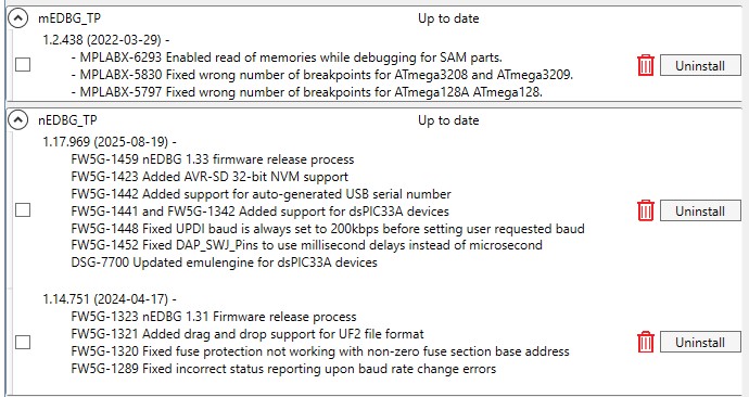
Software Update Liste mEDBG_TP nEDBG_TP
-1442 Added support for auto-generated USB serial number FW5G-1441 and FW5G-1342 Added support for dsPIC33A devices FW5G-1448 Fixed UPDl baud is always set to 200kbps before setting user requested baud FW5G-1452 Fixed DAP_SWJ_Pins to use millisecond delays instead of microsecond DSG-7700 Updated emulgine for dsPIC33A devices 1.14.751 (2024-04-17) - FW5G-1323 nEDBG 1.31 Firmware release process FW5G-1321 Added drag and drop support for UF2 file format FW5G-1320 Fixed fuse protection not working with non-zero
in „ATtiny416-Xplained Nano, Firmware Update“ · Mikrocontroller und Digitale Elektronik · · Screenshots
-
PDF
U13843EU3V0AN00.pdf
JP1 JP2 69.3 MHz 2 POD4 JP3 (Default) N C JP1 JP2 65.4 MHz JP3 JP1 JP2 62.0 MHz CN12 JP12 JP13 JP3 JP14 JP1 JP2 49.1 MHz CN42 JP3 CN13 6 P J CN7 CN14 UNB4111 Evaluation Board Jumper Settings Rev. 2.1d 2 V RC 4171A Graphics Display Controller LCD Controller The LCD controller is designed to work with a
in „Controller für Graphik LCD“ · Mikrocontroller und Digitale Elektronik ·
-
PDF
DTM_GHS_D_99.pdf
(10) einsetzen. Druckfeder (11) und die drei Sonnenräder • Achse umspannen (mit Andrehung (12, 13, 14) abnehmen. nach unten) • Nabe an der Achse umspannen! • Festkonus (35) abschrauben Danach: • Antreiber (34), Druckfeder (32), mit • großes Sonnenrad (14) montieren, Winkeldeckel (31), große Druckfeder
-
PDF
131-ripe2-2.pdf
0=res, 1=res, 2=internet, 3=res, 4=video, 5=L2 service, 6=voice, 7=management R Reserved a R1 Area 14 bit Indicates what R1 that the address is delegated from, max 16,384 R1 p R1 User 13 bit User identifier, max 8192 users u User subnet Delegated to user Examples: Source Destination PIESSS PIESSS ---
-
PDF
SCHALTUNG_DS1307_RTC.pdf
DS1307 RTC ) 7805 V IC2 +5V 1 0 10µ 10µ t LCD 2x16 Anmerkung: Diese LEDs könnten ev. Probleme bereiten r D n S / 0 1 2 3 4 5 6 7 16 V V K R R E D D D D D D D D k k 4 4 SDA Programmieradapter 1 5 1s SCL
in „DS1307 TWI I2C RTC Initialisierung ROM Zeit setzen auslesen Assembler ATmega8“ · Projekte & Code ·
-
PDF
LM3488.pdf
SL can be used to provide an additional method for setting the current limit. 2. On-resistance, R DS(ON) 3. Total gate charge, Qg POWER DIODE SELECTION Observation of the boost converter circuit shows that the av- 4. Reverse transfer capacitance, C RSS 5. Maximum drain to source voltage, V DS(MAX) erage
in „SEPIC LM3488“ · Analoge Elektronik und Schaltungstechnik ·
-
PDF
TMS320F2812_Board.pdf
3.3V/+5V/NC * 2 +3.3/+5V/NC * 3 XD0 4 XD1 5 XD2 6 XD3 7 XD4 8 XD5 9 XD6 10 XD7 11 XD8 12 XD9 13 XD10 14 XD11 15 XD12 16 XD13 17 XD14 18 XD15 19 XA0 20 XA1 21 XA2 22 XA3 23 XA4 24 XA5 25 XA6 26 XA7 27 XA8 28 XA9 29 XA10 30 XA11 31 XA12 32 XA13 33 XA14 34 XA15 35 GND 36 GND 37 XZCS0AND1n 38 XZCS2n 39 XREADY
in „Wieder eine Elektronik-Anfängerfrage“ · Mikrocontroller und Digitale Elektronik ·
-
PDF
Si_4322.pdf
alarm Low Power parts • Wireless keyboard/mouse and other PC peripherals 8 9 15 1 2 3 4 5 16 10 11 14 • Toy control CLK XTL ARSSI SDISCK nSEL SDO nIRQ nRES VSS VDD • Remote keyless entry • Tire pressure monitoring • Telemetry • Personal/patient data logging • Remote automatic meter reading Si4322-DS
in „RFM01 NIRQ immer high“ · Mikrocontroller und Digitale Elektronik ·
-
PDF
MC34151D.pdf
Enhanced System Performance with Common Switching Regulator 1 (SO–8) Control ICs Pin Out Equivalent to DS0026 and MMH0026 PIN CONNECTIONS N.C. 1 8 N.C. Representative Block Diagram LogicInputA2 7 DriveOutputA VCC 6 Gnd 3 6 VCC + LogicInputB4 5 DriveOutputB + – + + 5.7V (TopView) + DriveOutputA LogicInputA
in „Mosfet Treiber Baustein“ · Analoge Elektronik und Schaltungstechnik ·
-
Datei
AT32MENU_Int_anzeige_Abfrage_Passwort.bas
Echtzeituhr Ddrd = &HFE Ddrb.1 = 1 Config Sda = Portc.1 ' I2C Bus konfigurieren Config Scl = Portc.0 Const Ds1307w = &HD0 ' Addresse der Ds1307 Uhr Const Ds1307r = &HD1 Config Clock = User '' Interne Time/Date Routinen für Bascom konfigurieren Config Date = Dmy , Separator = . ' *********** Konfiguration Ende
in „Variabeln ändern in ISR“ · Mikrocontroller und Digitale Elektronik ·
-
PDF
Platinfuchs_IIa_Schematic-and-Layout.pdf
* *GND* *GND* GND GND GND GND GND *3V3* 3V3 VZK VZK U13 *3V3* *3V3* 16 1 K K C VDD2 VDD1 V V C L7 U14 C14 C15 *3V3* J2 8 1 15 2 3V3 22µF 22µF 15µH 1 R24 VCC RO B1 A1 16V 16V 6 B 1 MCSDC0604-150YU P 6 2 10R 7 B RE 2 14 B2 A2 3 U4A M S 74LVC14A D9 D10 C30 C31 3 R25 6 3 13 4 2 1 a485-en GND GND 10µF 4 A
in „Platinfuchs IIa: Isolierter, bidirektionaler 45W DC/DC Wandler zum Laden/Entladen eines Liion-Akkus“ · Projekte & Code ·
-
PDF
kicad_8450_dcm_liste_neu_v3.pdf
Interface, TSSOP20 DP83848C MII/RMII Single 10/100Mbps Ethernet Physical Layer Transciever, LQFP48 DS89C21 Differential CMOS Line Driver and Receiver Pair, SOIC-8 EL7242C Translateur TTL->VMOS. Double driver VMOS FUSB302B01MPX Fairchild USB Interface IC 302B Type-C Control IC with PD, MLP14D FUSB302B10MPX
in „KiCAD Eeschema, Bibliotheksdokumentation *.dcm als PDF-Datei“ · Platinen ·
-
PDF
L7200.PDF
Unit VICM INPUT COMMON MODE VCC/4 V RANGE +/-1.5 FODB UNITY GAIN BANDWIDTH 10 MHz VCM, POWER STAGE R DS(ON) Output On Resistance (Each Tj= 25°C 0.25 Device) Tj= 125°C 0.35 I Operating Current 1.3 A o O(LEAK) Output Leakage Current Vcc = 14V 1.0 mA VCM, CURRENT SENSE AMPLIFIER AV Voltage Gain 3.88 4 4.12
in „Externe Festplatte durch falsches Netzteil zerstört“ · PC Hard- und Software ·
-
PDF
lm2733.pdf
1.6-MHz (“X”), 0.6 MHz (“Y”) Switching frequency MHz (“X” option) and 600 kHz (“Y” option). • Low R DS(ON) DMOS FET The use of SOT-23 package, made possible by the • Switch current up to 1 A minimal power loss of the internal 1-A switch and use • Wide input voltage 2.7 V to 14 V of small inductors and
in „[V] 5 St. LM2733YMF Aufwärtswandler 1,6 MHz, 40-V-internem FET SOT-23 [7€)“ · Markt ·
-
PDF
ETEMB043013XDHAL_-_ver2.pdf
25C(CENTER TEST) gD di rgi nt me Do E 02101300-01-02 E TECHNOLOGIES CORPORAETEMB043013XDHALV2RSIP14E 14. INSPECTION CRITERIA 14.1 APPLICATION DELIVERED FROM EMERGING DISPLAY TECHNOLOGIES CORP.( E.D.T ) TO CUSTOMERS 1414.2(1)OBSERVATION D455cmE . (2)VIEWING A45 nly 90 (FOR SECTION OUTSIDE OF VnEWING
in „EDT Display Interface mit STM32F7“ · Mikrocontroller und Digitale Elektronik ·
-
PDF
Schaltplan.pdf
1 2 3 4 X5 schwarz 1 rot 2 gelb C14 3 100n JST B3B-EH_A X2 X6 GND 1 A +24V 2 A D3 LM2576 +12V...6V 2 L1 C15 3 1 OUT 100n JST B3B-EH_A +24V Vin 4 V3 150µH C9 C10 R9 X7 C8 Feedback 1N5818 470u 470u 18k 100u GND ON/OFF 1 2 3 5 3 D4 TPS5420D
in „ATtiny2313 ungewollter Reset?“ · Mikrocontroller und Digitale Elektronik ·