-
PDF
LTC1477_LinearTechnology.pdf
0.254mm) PER SIDE RELATED PARTS PART NUMBER DESCRIPTION COMMENTS LTC1153 Electronic Circuit Breaker MOSFET Driver with Adjustable Reset Time LTC1154 Single High Side Driver MOSFET Driver with Switch Status Output LTC1155 Dual High Side Driver Dual MOSFET Driver with Protection LTC1470 5V and 3.3V V Switch
in „TPS61175 Overccurent Protection Mode“ · Analoge Elektronik und Schaltungstechnik ·
-
PDF
MAX6457-MAX6460.pdf
applications. Figure 9 shows a typical circuit for RPULLUP OUT this application using a pass P-channel MOSFET. The MAX6458 OUT MAX6457–MAX6460 are powered directly from the sys- ONLY tem voltage supply. Select R1 and R2 to set the trip R1 voltage (see the Programming the Trip Voltage (V TRIP ) IN+ VCC section
in „Tiefenentladungsschutz für Li-Ion Akku mit MAX6457“ · Analoge Elektronik und Schaltungstechnik ·
-
PDF
si1402dh.pdf
Si1402DH Vishay Siliconix N-Channel 30 V (D-S) MOSFET FEATURES PRODUCT SUMMARY • Halogen-free According to IEC 61249-2-21 VDS (V) RDS(on)(Ω) D (A) Definition 0.077 at V = 4.5 V 3.4 30 GS TrenchFET Power MOSFET: 2.5 V Rated 0.120 at GS= 2.5 V 2.5 Compliant
-
PDF
DSE-CN5711.pdf
Operating Voltage Range: 2.8V to 6V operating from an input voltage of 2.8V to 6V, the On-chip Power MOSFET constant output current can be set up to 1.5A with an Low Dropout Voltage: 0.37V @ 1.5A external resistor. The CN5711 is ideal for driving LED Current up to 1.5A LED. The on-chip power MOSFET and
in „LED Treiber Input 5VDC Output 2V 400mA bis 800mA gesucht“ · Mikrocontroller und Digitale Elektronik ·
-
PDF
IXIS_24N100Q3.pdf
Q3-Class V = 1000V IXFK24N100Q3 DSS TM HiperFET IXFX24N100Q3 ID25 = 24A Power MOSFET R 440m DS(on) D t 300ns rr N-Channel Enhancement Mode G Avalanche Rated TO-264 (IXFK) Fast Intrinsic Rectifier S G Symbol Test Conditions Maximum Ratings DS VDSS TJ= 25C to 150C 1000 V Tab V
in „SMA SB4200TL-MS Reparatur“ · Analoge Elektronik und Schaltungstechnik ·
-
PDF
bom-v1-0.pdf
, 80V, 1A, 1W BCX 56-16 NXP 0,15 € 0,15 € Q21, Q22, Q25, Q52, Q60, Q61, Q62, Q90, Q91, 11BSS138, Mosfet, N, 0.36A, 60V BSS 138P NXP 0,06 € 0,66 € Q23, Q24, Q50, Q51, Q120 5IRLML 6402, Mosfet, P, 3.7A, 20V IRLML 6402 0,25 € 1,25 € Q100, Q101, Q102, Q103 4BC 817, SMD, NPN, 0.5A BC 817-25 SMD 0,02 € 0,08
in „Universalplatine für STM32, grobe Fehler vor der Herstellung?“ · Mikrocontroller und Digitale Elektronik ·
-
PDF
Littelfuse_Discrete_MOSFETs_N-Channel_Standard_IXT_1N450HV_Datasheet.PDF.pdf
High Voltage IXTT1N450HV V = 4500V DSS Power MOSFET IXTH1N450HV ID25 = 1A R 80 DS(on) N-Channel Enhancement Mode TO-268HV (IXTT) G S D (Tab) Symbol Test Conditions Maximum Ratings TO-247HV (IXTH) V DSS TJ= 25C to 150C 4500 V V DGR TJ= 25C to
in „SOA Diagramm richtig anwenden“ · Analoge Elektronik und Schaltungstechnik ·
-
PDF
vt6k1.pdf
Data Sheet 1.2V Drive Nch + Nch MOSFET VT6K1 Structure Dimensions (Unit : mm) Silicon N-channel MOSFET VMT6 4 1.2 0.5 0 (6)(5) (4) Features . . 1) Low on-resistance. 1 0 2) Small package(VMT6). (1)(2) (3) 4 0.160.13 3) Low voltage drive
in „Bitte um Hilfe Bauteilsuche“ · Analoge Elektronik und Schaltungstechnik ·
-
PDF
DRV8711.pdf
microstepping The DRV8711 device is a stepper motor controller motor driver that uses external N-channel MOSFETs to drive a bipolar stepper motor or two brushed DC motors. A – Built-In 1/256-Step microstepping indexer microstepping indexer is integrated, which is capable – Drives external N-Channel MOSFETs of
in „DRV8711 Schrittmotortreiber Fehler“ · Analoge Elektronik und Schaltungstechnik ·
-
PDF
Datasheet_DRV8711.pdf
microstepping The DRV8711 device is a stepper motor controller motor driver that uses external N-channel MOSFETs to drive a bipolar stepper motor or two brushed DC motors. A – Built-In 1/256-Step microstepping indexer microstepping indexer is integrated, which is capable – Drives external N-Channel MOSFETs of
in „DRV8711 Steppermotortreiber - Hohe Geschwindigkeiten“ · Analoge Elektronik und Schaltungstechnik ·
-
PDF
UC3842B.pdf
orsinkhighpeakcurrent.Theoutputstage,suitable . LOWSTART-UPAND OPERATINGCURRENT for driving N-Channel MOSFETs, is low in the off- state. Differences between members of this family are the DESCRIPTION under-voltage lockout thresholds and maximum duty TheUC384xBfamilyofcontrolICsprovidesthenec- cycle ranges
in „Reparatur Schaltnetzteil“ · Analoge Elektronik und Schaltungstechnik ·
-
PDF
uc3842b.pdf
orsinkhighpeakcurrent.Theoutputstage,suitable . LOWSTART-UPAND OPERATINGCURRENT for driving N-Channel MOSFETs, is low in the off- state. Differences between members of this family are the DESCRIPTION under-voltage lockout thresholds and maximum duty TheUC384xBfamilyofcontrolICsprovidesthenec- cycle ranges
in „40-390V HV DC-DC-Wandler vom Chinamann“ · Analoge Elektronik und Schaltungstechnik ·
-
PDF
MWE_RSD-30-SERIE_DB-EN.pdf
CONQUE MST, 3.15A, 250V H Time-Lag CONQUE MST, 2A, 250V Input Reverse Polarity Protection There is a MOSFET connected in series to the negative input line. If the input polarity is connected reversely, the MOSFET opens and there will be no output to protect the unit. Input Range and TransientAbility The
in „Kindereisenbahn hohe Stromspitzen begrenzen“ · Fahrzeugelektronik ·
-
PDF
Diplomarbeit_24_Kanal_EEG_Recorder.pdf
des N-Kanal Mosfet Q6 auf high gesetzt, wird der P-Kanal Mosfet Q1 durchgeschaltet. Laut Datenblatt ist mit einem R onn weniger als 0,3 Ohm zu rechnen und damit liegt der Spannungsabfall bei großzügig angenommenen 50mA
in „EEG-Kappen-Controller“ · Mikrocontroller und Digitale Elektronik ·
-
PDF
tps2020_1_.pdf
SLVS175B − DECEMBER 1998 − REVISED MARCH 2004 D 33-mΩ (5-V Input) High-Side MOSFET D OR P PACKAGE Switch (TOP VIEW) D Short-Circuit and Thermal Protection GND 1 8 OUT D Overcurrent Logic Output IN 2 7 OUT D Operating Range . . . 2.7 V to 5.5 V IN 3 6 OUT D Logic-Level Enable Input
in „DC/DC als Sicherung für AT90USB <-> PC“ · Mikrocontroller und Digitale Elektronik ·
-
PDF
RDR-158.pdf
RDR-158 – 5 V, 1 A, LNK616PG CV/CC Charger The LNK616PG monolithically integrates the 700 V power MOSFET switch and controller. A unique ON/OFF control scheme provides CV regulation. The IC also incorporates both output cable voltage-drop compensation and tight regulation over a wide temperature range
in „Trafo oder schaltnetzteil“ · Analoge Elektronik und Schaltungstechnik ·
-
PDF
NCP1271-D.PDF
− 5 Drv Driver Output The NCP1271’s powerful output is capable of driving the gates of large Qg MOSFETs. 6 V Supply Voltage This is the positive supply of the device. The operating range is between 10 V (min) and CC 20 V (max) with a UVLO start threshold 12.6 V (typ). 8 HV High Voltage This pin provides
in „Behringer B112D Funktionsweise Netzteil“ · Analoge Elektronik und Schaltungstechnik ·
-
Datei
PWMs.txt
Globale Variable long duty, w1, w2, w3; //Duty Cycle der PWMs void rechtskom (){ // Für die High-Mosfets wird das Dutycycle auf duty für high und auf 0 für Low eingestellt (PWM nur für High MosFets) if ( PINB & (1<<PINB0) ) { if ( !(PINB & (1<<PINB1))) { w1=duty;;//Ausgang high Diode aus } else{w1=0;
in „zwei if-Anweisungeg funktionieren nicht zusammen“ · Mikrocontroller und Digitale Elektronik ·
-
PDF
STD5NM50.pdf
STD5NM50 STD5NM50-1 N-CHANNEL 500V - 0.7 - 7.5A DPAK/IPAK MDmesh™Power MOSFET TYPE VDSS R DS(on) ID STD5NM50 500V <0.8 7.5 A STD5NM50-1 500V <0.8 7.5 A n TYPICAL R DS(on) = 0.7 n HIGH dv/dt AND AVALANCHE CAPABILITIES 3 3 2 n 100% AVALANCHE TESTED 1 1 n LOW INPUT CAPACITANCE
in „Dynamischer Wärmewiderstand => Cth Rth“ · Analoge Elektronik und Schaltungstechnik ·
-
PDF
FDN335N.pdf
F D April1999 N 3 3 5 N FDN335N N-Channel 2.5V Specified PowerTrench TM MOSFET General Description Features This N-Channel 2.5V specified MOSFET is produced • 1.7 A, 20 V. DS(ON)0.07 @ V GS = 4.5 V usingFairchildSemiconductor'sadvancedPowerTrench R = 0.100 @ V = 2.5 V. processthathasbeenespeciallytailoredtominimize
in „FDN335N Hilfe mit dem Datenblatt“ · Mikrocontroller und Digitale Elektronik ·
-
PDF
FDN335N.pdf
F D April1999 N 3 3 5 N FDN335N N-Channel 2.5V Specified PowerTrench TM MOSFET General Description Features This N-Channel 2.5V specified MOSFET is produced • 1.7 A, 20 V. DS(ON)0.07 @ V GS = 4.5 V usingFairchildSemiconductor'sadvancedPowerTrench R = 0.100 @ V = 2.5 V. processthathasbeenespeciallytailoredtominimize
in „Batt. Ladung per MOSFET Ein/Aus schalten“ · Mikrocontroller und Digitale Elektronik ·
-
PDF
DS100258D_IXTH-TT16N10D2_.pdf
Depletion Mode IXTT16N10D2 V DSX = 100V MOSFET IXTH16N10D2 I > 16A D(on) R DS(on) 64m D N-Channel G TO-268 (IXTT) S G S D (Tab) Symbol Test Conditions Maximum Ratings TO-247 (IXTH) VDSX TJ= 25C to 175C 100 V V T = 25C to 175C, R = 1M 100
in „Wann sperrt ein selbstleit. N-Kanal MOSFET?“ · Analoge Elektronik und Schaltungstechnik ·
-
PDF
tk18a60v_en_datasheet_110131.pdf
TK18A60V MOSFETs Silicon N-Channel MOS (DTMOS) TK18A60V 1. Applications • Switching Voltage Regulators 2. Features (1) Low drain-source on-resistance: RDS(ON)= 0.165 Ω (typ.) by used to Super Junction Structure :
in „Mosfet defekt - kann der Ersatztyp verwendet werden?“ · Analoge Elektronik und Schaltungstechnik ·
-
PDF
tps65136.pdf
Sequencing delay Vposstart to negstart 6 8.7 11 ms V Feedback ground regulation –10 0 10 mV FBG M1 MOSFET on-resistance sw = 100 mA 200 M2 MOSFET on-resistance sw = 100 mA 400 rDS(on) mΩ M3 MOSFET on-resistance sw = 100 mA 900 M4 MOSFET on-resistance I = 100 mA 600 sw SW Switch current limit (M2) Vin 3.7
in „OLED Sammelbestellung“ · Markt ·
-
PDF
Designing_a_digital_compass.pdf
to the current demand. For this In this application note, we chose the dual axis application, the MOSFET receives the current directly MXD2020EL available from MEMSIC (see “Refer- from the 9V battery (see Figure B-2). This is known as ences”), which has a range of ±1g and an operating the Set/Reset strap
in „Kompassmodul HDMM01 von Pollin“ · Mikrocontroller und Digitale Elektronik ·
-
PDF
MC33153-D.pdf
driving discrete and module IGBTs, this device offers a cost effective solution for driving power MOSFETs and Bipolar http://onsemi.com Transistors. Device protection features include the choice of desaturation or overcurrent sensing and undervoltage detection. These MARKING devices are available in dual
in „Treiber für MOSFET Brücke mit eingebauten Kurzschlußschutz gesucht“ · Analoge Elektronik und Schaltungstechnik ·
-
Datei
Fehler.txt
100n TC=0,0 X_M1 N16994 N15150 0 IRF530N **** RESUMING Test.cir **** .END WARNING -- LAMBDA for MOSFET model X_M1.MM is unusually large and might cause nonconvergence **** 03/08/12 19:01:12 ******* PSpice 16.3.0 (June 2009) ****** ID# 0 ******** ** Profile: "SCHEMATIC1-Test" **** Diode MODEL PARAMETERS
in „IRF2127 Beschaltung“ · Analoge Elektronik und Schaltungstechnik ·
-
PDF
SG6841V2.1.pdf
Sense current limiting. 7 VDD Power supply Power Supply. The totem-pole output driver for the power MOSFET. A soft driving waveform is 8 GATE Driver Output implemented to improve EMI. ©System General Corp. - 2 - www.sg.com.tw Version 2.1 (IRO33.0001.B5) Jun.15,2006 Product Specification High-integrated
in „SNT fiept im Leerlauf“ · Analoge Elektronik und Schaltungstechnik ·
-
PDF
564746-da-01-en-MOSFET_N_KA_800V_STP4N80K5_TO_220AB_STM.pdf
STD4N80K5, STF4N80K5, STP4N80K5, STU4N80K5 N-channel 800 V, 2.1 Ω typ., 3 A MDmesh™ K5 Power MOSFETs in DPAK, TO-220FP, TO-220 and IPAK packages Datasheet - production data Features TAB Order code VDS RDS(on)max. D PTOT 3 1 STD4N80K5 60 W DPAK 3 12 STF4N80K5 20 W TO-220FP 800 V 2.5 Ω 3 A TAB STP4N80K5
in „Anodenspannungsstabilisierung für Röhrenverstärker mit IRF840 als Längsregler“ · Analoge Elektronik und Schaltungstechnik ·
-
PDF
en.CD00004215.pdf
combines a state-of-the-art PWM circuit along with an optimized 700 V avalanche rugged Vertical Power MOSFET. It is part of STMicroelectronics’ proprietary VIPower, (Vertical Intelligent Power). It uses a fabrication process, which allows the integration of analog control circuits with vertical power device
in „Schaltnetzteil - Viper50A-E 45W“ · Analoge Elektronik und Schaltungstechnik ·
-
PDF
vo3120.pdf
VO3120 www.vishay.com Vishay Semiconductors 2.5 A Output Current IGBT and MOSFET Driver FEATURES • 2.5 A minimum peak output current NC 1 8 V • 25 kV/μs minimum common mode rejection CC (CMR) at VCM = 1500 V A 2 7 VO • CC = 2.5 mA maximum supply current C 3 6 V • Under voltage
in „MOSFET High side Treiber“ · Analoge Elektronik und Schaltungstechnik ·
-
PDF
NFAQ1060L33T-D.PDF
. 1 nF, the FAULT output is switched on for 1.65 ms (typ.) The internal bootstrap circuit uses a MOSFET. The turn because the FAULT pin goes back to high impedance when CFOD is higher than 8 V (typ.). on time of this MOSFET is synchronized with the turn on of the low side IGBT. The bootstrap capacitor
in „Ersatz für ON-Semi STK5Q4U362J-E / STK5Q4U363J-E bzw. passt da NFAQ1060L33T / NFAQ1060L36T“ · Analoge Elektronik und Schaltungstechnik ·
-
PDF
STK5Q4U362J-E-D.PDF
RCIN pin. If RCLR = 2 MΩ and CCLR = 1 nF, the FAULT output The internal bootstrap circuit uses a MOSFET. The is switched on for 1.65 ms (typical). turn on time of this MOSFET is synchronized with the turn on of the low side IGBT. The bootstrap capacitor is charged by turning on the low side IGBT. The
in „Ersatz für ON-Semi STK5Q4U362J-E / STK5Q4U363J-E bzw. passt da NFAQ1060L33T / NFAQ1060L36T“ · Analoge Elektronik und Schaltungstechnik ·
-
PDF
Ladungsverst_rker_1.PDF
Verstärkereingang mit einem oder Reed-Relais verwendet, welche nach zusätzlich in Serie eingebautem MOSFET realisiert. Die besten zur Zeit normalerweise im stromlosen Zustand WiderstandR TP imKabeleinenTiefpass- erhältlichen MOSFET haben einen Ein- geschlossen sind. Dies um eine Be- filter. gangsleckstrom
-
Datei
UselessBox.c
PB5) myservo1.attach(12); // servo an pin 12 zum servoobejekt(PB4) pinMode(8, OUTPUT); // für den MOSFET pinMode(2, INPUT); // Schalterunterbrechung digitalWrite(2, HIGH); myservo2.write(S2fra); myservo1.write(S1fra); delay(600); digitalWrite(8, HIGH); delay(300); digitalWrite(8, LOW); //alle unbenutzen
in „Promgrammfehler in Arduino“ · Mikrocontroller und Digitale Elektronik ·
-
PDF
irl630.pdf
PD -9.1255 IRL630 HEXFET Power MOSFET Dynamic dv/dt Rating RepetitiveAvalancheRated Logic-Level Gate Drive V DSS = 200V RDS(ON) Specified at V GS = 4V & 5V 150°C Operating Temperature R DS(on) = 0.40 FastSwitching Ease of paralleling ID
in „Kontrolle der Kühlkörperberechnung“ · Mikrocontroller und Digitale Elektronik ·
-
PDF
ZXMN2B01F.pdf
ZXMN2B01F 20V SOT23 N-channel enhancement mode MOSFET with low gate drive capability Summary V(BR)DSS RDS(on)(⍀) ID(A) 0.100 @ V GS= 4.5V 2.4 20 0.150 @ V = 2.5V 2.0 GS 0.200 @ V GS= 1.8V 1.7 Description This new generation trench MOSFET from Zetex features
in „LED-Spannungswandler mit MOSFET ?“ · Mikrocontroller und Digitale Elektronik ·
-
PDF
datasheet.pdf
STP22NF03L N-channel 30V - 0.0038Ω- 22A - TO-220 STripFET™ II Power MOSFET Features Type VDSS RDS(on) D STP22NF03L 30V <0.05Ω 22A ■ Exceptional dv/dt capability ■ Low gate charge at 100°C 3 ■ Application oriented characterization 2 1 ■ 100% avalanche tested TO-220 Application ■ Switching applications Description Figure 1. Internal schematic diagram This Power MOSFET is the latest development of STMicroelectronics unique "single feature size" strip-based process. The resulting transistor shows extremely high packing density for low on- resistance, rugged avalanche
in „Unbekannter Spannungsregler von ST“ · Analoge Elektronik und Schaltungstechnik ·
-
PDF
FD6287T_cn-translated.pdf
FD6287T is an integrated three independent half-bridge - Suspension absolute voltage +250V dynamic MOSFET design O,rperates up to +250V.for high voltage, high speed dri-e Integrates three independent half-bridge drivers FD6287T built-in VCC/VBS undervoltage (UVLO) protection - Output current +1.5A/-1.8A
in „PWM: Motortreiber schaltet bei Tastverhältnis Reduktion ab“ · Analoge Elektronik und Schaltungstechnik ·
-
PDF
APM2601.pdf
APM2601 P-Channel Enhancement Mode MOSFET Features Pin Description • -20V/-3A , RDS(ON)80mΩ(typ.) @ V =GS.5V D 1 6 D R =110mΩ(typ.) @ V =-2.5V DS(ON) GS D 2 5 D • Super High Dense Cell Design for Extremely G 3 4 S Low R DS(ON) • Reliable and
in „SMD-Bauteilbestimmung“ · Mikrocontroller und Digitale Elektronik ·
-
PDF
IXTA-TP3N50D2_.pdf
Depletion Mode IXTA3N50D2 V DSX = 500V MOSFET IXTP3N50D2 I > 3A D(on) R DS(on) ≤ 1.5 Ω N-Channel TO-263 AA (IXTA) G Symbol Test Conditions Maximum Ratings S VDSX TJ= 25°C to 150°C 500 V D (Tab) VGSX Continuous ±20 V V Transient ±30 V TO-220AB
in „J-FET N-Channel mit gößer 70V Drain / Source Spannung für Konstantstromsenke“ · Analoge Elektronik und Schaltungstechnik ·
-
PDF
DS100728A_IXTN660N04T4_-1022876.pdf
Advance Technical Information TrenchT4 TM IXTN660N04T4 V = 40V DSS Power MOSFET ID25 = 660A R DS(on) 0.85m D N-Channel Enhancement Mode G Avalanche Rated S S Fast Intrinsic Diode miniBLOC, SOT-227 E153432 S Symbol Test Conditions Maximum Ratings G VDSS TJ= 25C to 175C 40
in „Suche Power-MosFet für etwa 600A“ · Analoge Elektronik und Schaltungstechnik ·
-
PDF
APT34F100B2_L_D-1593638.pdf
N-Channel FREDFET T-Max Power MOS 8 ™ is a high speed, high voltage N-channel switch-mode power MOSFET. TO-264 This 'FREDFET' version has a drain-source (body) diode that has been optimized for high reliability in ZVS phase shifted bridge and other circuits through redurrd t , soft recovery, and high
in „SMA SB4200TL-MS Reparatur“ · Analoge Elektronik und Schaltungstechnik ·
-
PDF
FDC638P-D.PDF
F D C 6 3 8 P FDC638P Ò P-Channel 2.5V PowerTrench Specified MOSFET General Description Features This P-Channel 2.5V specified MOSFET is produced • –4.5 A, –20 V.R DS(ON)= 48 mΩ @ V GS= –4.5 V using ON Semiconductor’s advanced PowerTrench process that has been especially
in „richtiger n-Kanal MOSFET, 3,3V soll 5V und 100mA schalten“ · Analoge Elektronik und Schaltungstechnik ·
-
PDF
IRF4905.pdf
PD-91280D IRF4905 HEXFET Power MOSFET l Advanced Process Technology l Ultra Low On-Resistance D l Dynamic dv/dt Rating V DSS = -55V l 175°C Operating Temperature l Fast Switching R DS(on) = 0.02Ω G l P-Channel l FullyAvalancheRated S ID
in „P Kanal Mosfet schlägt immer wieder mal Durch.“ · Analoge Elektronik und Schaltungstechnik ·
-
PDF
ttester.pdf
. . . . . . . . . . . . . . . . . . . 38 5.1.1 Messung eines PNP-Transistors oder eines P-Kanal MOSFETs . . . . . . . . . 39 5.1.2 Messung eines NPN-Transistors oder eines N-Kanal-MOSFET . . . . . . . . . 40 5.1.3 Vereinfachter Ablauf der Transistorerkennung . . . . . . . . . . . . . . . . . . 43 5.1.4
-
PDF
LTC6802-1.pdf
undervoltage conditions. A standby mode is also provided. APPLICATIONS Each cell input has an associated MOSFET switch for n Electric and Hybrid Electric Vehicles discharging overcharged cells. n High Power Portable Equipment n Backup Battery Systems For largebatterystackapplicationsrequiringindividually addressable
in „SPI: kein SCK bei Receive - Warum?“ · Mikrocontroller und Digitale Elektronik ·
-
 Bild
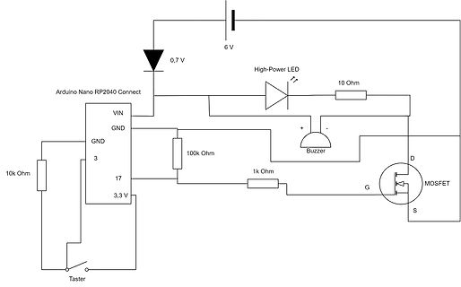
Schaltplan mit Arduino Nano RP2040 Connect, LED, MOSFET und Buzzer
0,7 V, High-Power LED, 10 Ohm, Arduino Nano RP2040 Connect, VIN, GND, Buzzer, 100k Ohm, 1k Ohm, MOSFET, D, G, S, 3, 17, 3,3 V, 10k Ohm, Taster
in „Schaltung mit Arduino Nano RP2040 Connect funktioniert auf Steckbrett, aber nicht gelötet“ · Platinen · · Schaltpläne