das mit 3 dieser Boards getestet. Aktuell lese ich alle Register aus die Ergebnisse: RTD Low Fault Threshold High Fault Threshold LSB 84 0 255 MSB 65 0 255 RTD gesamt 8362 //RTD = ((msb_rtd << 7)+((lsb_rtd & 0xFE) >> 1)); Faultstatus= 0 hat jemand ne Idee warum
(HIGH) erkannt werden.) PS: Ich habe schon mehrere ähnliche Näherungsschalter von Markenherstellern gemessen. Üblicherweise ist die Wiederholgenauigkeit der Schaltabstände deutlich unter 50 µm.
Eingang einstellt, ist allerdings auch nicht bekannt. Wir wissen auch noch nicht, welcher Pegel (High oder Low) nicht erkannt wird, sondern nur, dass "der Drucker nicht reagiert". Schaltschwelle und Eingangsstrom sind auch nicht bekannt. Oder die Schaltung auf der Platine braucht einen Näherungsschalter
conditions for auto-restart described above, if the If the primary magnetizing inductance is either too high or low the sensed FEEDBACK pin current during the forward period of the converter will automatically compensate for this by adjusting the conduction cycle (switch “on” time) falls below 120 mA, the
conditions : 温度 Temperature : 95±2℃ 時間 Time : 1000時間 1000 hours 6-6 低温試験 Low temperature test 以下の条件で試験後25℃にて24時間放置後の40kHzに於ける 音圧の変化:±3dB以内 The variation of the sound pressure level at 40.0kHz is within ±3dB compared with initial figures at 25℃ in 24 hours after following test
: 温度 Temperature : 95±2℃ 時間 Time : 1000時間 1000 hours 6-6 低温試験 Low temperature test 以下の条件で試験後25℃にて24時間放置後の40kHzに於ける 感度の変化:±3dB以内 The variation of the sensitivity at 40.0kHz is within ±3dB compared with initial figures at 25℃ in 24 hours after following test conditions
Ein LDO ist ein Low Drop Regler, der speziell mit geringem Spannungsabfall zwischen Eingang und Ausgang noch funktioniert. 10V sind aber fernab von "gering". Anhand dieser Fragestellung vermute ich, dass du Anfänger
Lothar M. schrieb im Beitrag #7810029: > Ein LDO ist ein Low Drop Regler, der speziell mit geringem > Spannungsabfall zwischen Eingang und Ausgang noch funktioniert. 10V sind > aber fernab von "gering". > > Anhand dieser Fragestellung vermute ich, dass
Serial.println(value); // Warte eine kurze Zeit delay(10); digitalWrite(en[mux], HIGH); } } // Deaktiviere den aktuellen Multiplexer digitalWrite(en[mux], HIGH); delay(100); } }[/code] Merkwürdigerweise zeigt der serielle Monitor unter anderem,
mux < 8; mux++) > { > // Aktiviere den aktuellen Multiplexer > digitalWrite(en[mux], LOW); .... aktiviert und dann wieder die 16 > Eingänge ausgelesen. Die Zeile digitalWrite(en[mux], HIGH); Steht dort zweimal! Einmal in der for Schleife für die Kanäle (dort ist sie falsch)
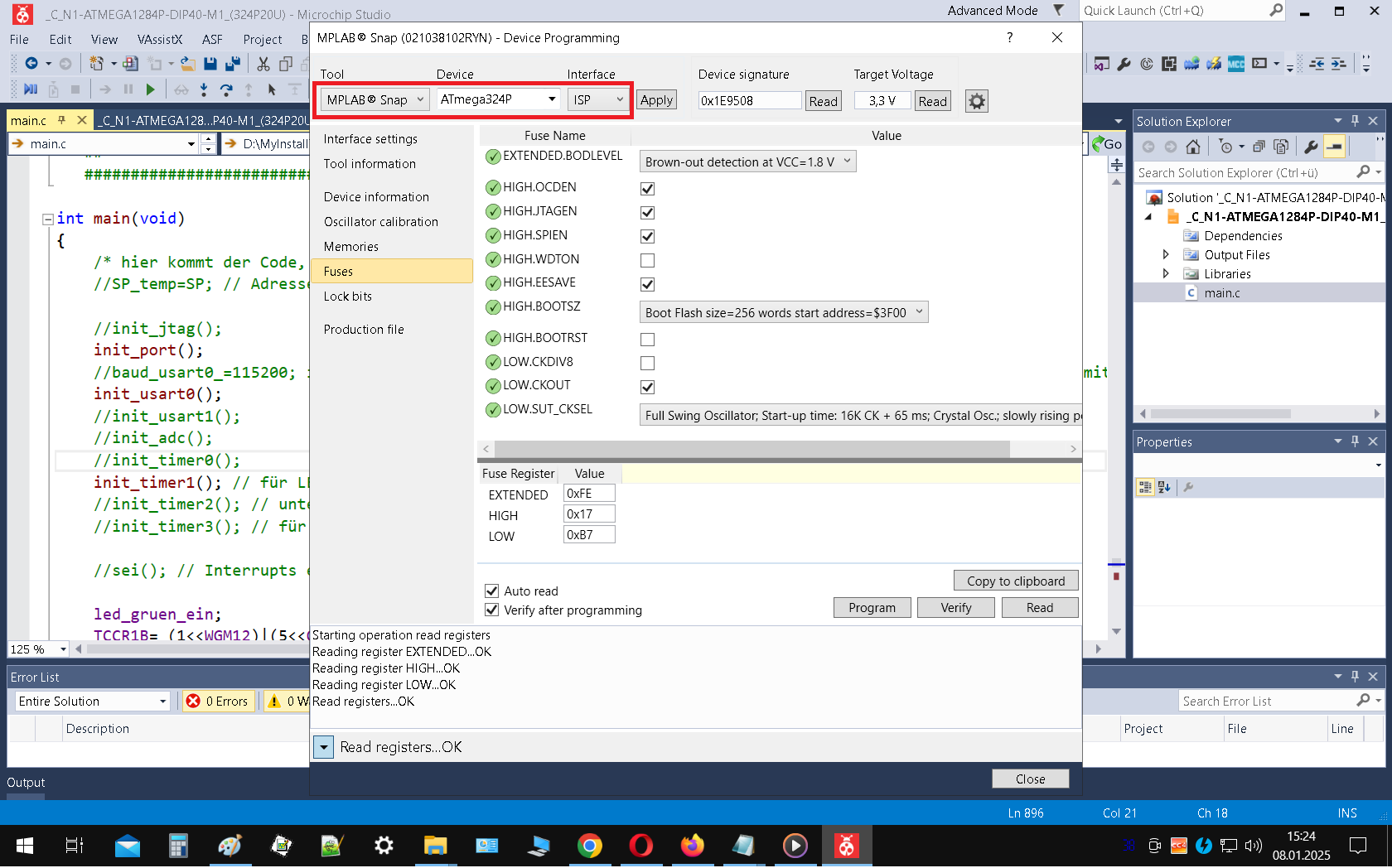
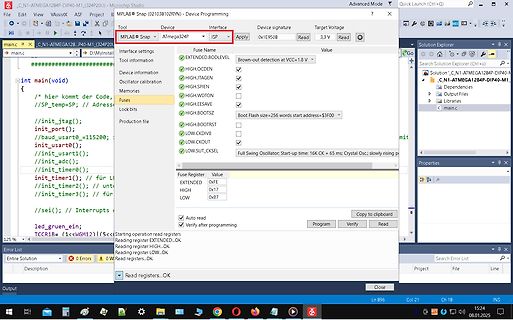
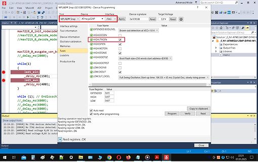
auch, "SPI programmers need the RESET pin to flash the device." "The only way to recover is with a high voltage programmer". https://www.mikrocontroller.net/articles/AVR_Fuses#SPIEN,_DWEN_und_RSTDISBL "Besonders heimtückisch"
Manfred H. schrieb im Beitrag #7809848: > Die Ausgänge sind bei aktiv auf Dauer high. Das kann man bei dem Board einstellen wie sich die Ausgänge verhalten. Anleitung lesen.
LITE-ON TECHNOLOGY CORPORATION Property of LITE-ON Only FEATURES * AC input response * High input-output isolation voltage ( Viso=5,000Vrms ) * Low collector dark current -7 ( CEO : MAX. 10 A at V CE =20V ) * Current transfer ratio ( CTR : MIN. 20% at I F=±1mA, V CE=5V ) * Response time (
extern für Ausgangsfunktionen Sinus, Pen-Lift-Ausgänge Dreieck, Rechteck TTL-Pegel, PENLIFT active high und PENLIFT INVERS Frequenzbereich des Trägers active low beim schnellen Rückfall der OCV-Spannung 1 mHz ... 22 MHz (TOE 7708A, TOE 7711A) auf die Startfrequenz Modulation intern Modulationsfrequenz
Register über das der Speicher adressiert werden kann. Das 16 Bit Register ist aufgeteilt in ein High und Low Register, damit über 8-Bit Zugriffe das Register beschrieben werden kann. Bei einem 32-Bitter (Wortbreite 32 Bit) wären bei einer Adressierung des Speichers mit 32 Bit ein Adressraum von
lightweight design and low power power-on. (For the operational consumption permit easy installation in a conditions, refer to the separate manual variety of equipment. ‘Dot Matrix LCD Unit with Built-In Controllers.’) • Allowing
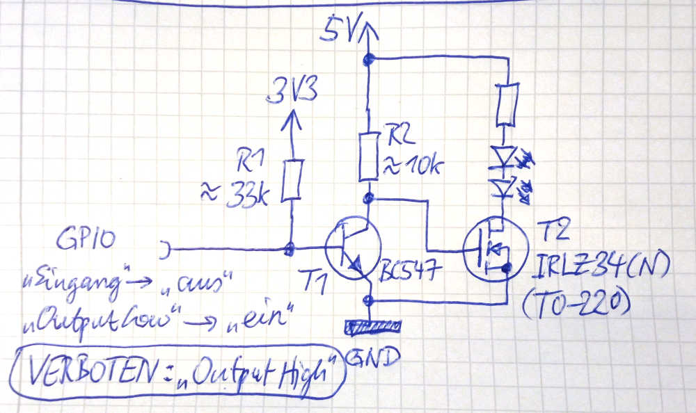
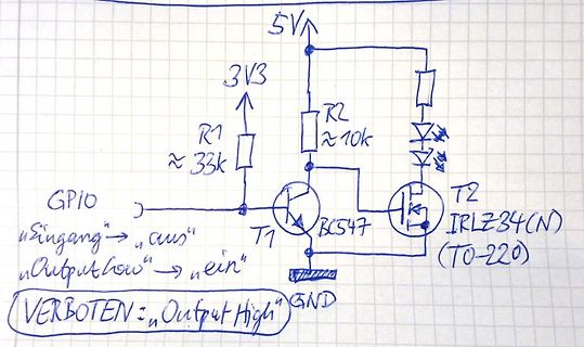
FET geht natürlich auch ein IRLZ44N). Der Eingang darf wegen des fehlenden Basiswiderstandes nicht high getrieben werden, nur entweder tri-stated (dann Last aus) oder auf low gezogen (dann Last ein). Habe ich bisher nicht praktisch ausprobiert, sollte aber so funktionieren, denke ich. Es sollte aber noch
muss, im Vergleich zum Transistor. Wenn ihr euch einig seid, dass ich etwas übertreibe mit meinem High Side, dann sollte ich mich wohl auch grundsätzlich auf Low Side einlassen. Wenn ich das richtig rausgelesen habe, gäbe es bei Variante 2 (low-side) allerdings noch die Herausforderung, einen passenden
signal is freely adjustable up to 15 MHz for flexible and fast data transmission. This combination of low power consumption and high adaptability makes the dual-wire ICLEDs particularly attractive for modern smart lighting applications. [/c] Interessant ist außerdem, dass der Spannungsbereich weit
on-resistance (the resistance between the drain and source when the MOSFET is on) by 30 percent. The lower on-resistance contributes to much lower power loss in customer designs. The REXFET-1 process also enables the new MOSFETs to offer a 10 percent reduction in Qg characteristics (the amount of charge
> Ich würde vermuten, Version B ist die bessere Variante, oder? Bei B ist die Leitung entweder high oder offen, bei A ist durch den 10k wenigstens etwas low gegeben.
diesmal möchte ich das gleiche Problem lösen, aber statt TL/TLC77… nun mit TPS61010 (boost Wandler mit low-bat Ausgang). Der TPS erzeugt ein low, wenn die per Spannungsteiler eingestellte Schwelle erreicht wird. Da ich das Buzzersignal vom Atmega ohnehin invertieren muss, kann ich diesen Transistor nutzen
this vulnerability, the method of exploiting it, and avenues for deducing more about the relevant low-level hardware behavior. --- via https://media.ccc.de/v/38c3-hacking-the-rp2350 [/c] Noch gibt es keine offiziellen Aussagen von Seiten der Raspberry Foundation - unter der als Quelle genannten
besuchen, um mehr zur Thematik zu erfahren. ### Portenta Proto Kit ME-Prototyping-Kit für High-End-Arduinos Der Verkauf von Kits ist seit jeher ein gewinnbringendes Verfahren, kostet das Kit doch meist mehr als die Summe seiner Teile. Nun gibt es ein neues Kit, das auf die Pro-Variante Portenta
Host agieren und ist komplizierter zu programmieren. Das OTG_HS-Modul unterstützt zusätzlich USB High Speed (480 MBit/Sec). Hier wird ein Controller mit der einfachsten Variante gewählt, der STM32F103RB. Dieser ist beispielsweise auf dem Olimexino-STM32 zu finden, im Folgenden wird dieses als Grundlage
nach Empfang eines IDLE-Frames, d.h. wenn für (mindestens) die Dauer eines Frames die Leitung auf 'High' war. Dies hat den Nachteil, dass zu Beginn einer schnellen Kommunikation die Effizienz sinkt. Auf eine genauere Erläuterung der USART-Ansteuerung wird hier verzichtet, weil dies nicht mehr viel mit
, 600V/µs Op Amps U FEATURES DESCRIPTIO ■ 25MHz Gain Bandwidth The LT1358/LT1359 are dual and quad low power high ■ 600V/µs Slew Rate speedoperationalamplifierswithoutstandingACandDC ■ 2.5mA MaximumSupply Current per Amplifier performance. The amplifiers feature much lower supply ■ Unity-Gain Stable
Warburg impedance effectively becomes zero. On the other hand, at low frequencies, only the effects of resistors and the Warburg element remain. The impedance spectrum also marks the following frequencies at critical points: w , w , w , w , and w . The lowest and highest
Solarzelle sein. Wenn man zusätzlich täglich per Kabel laden kann geht das schon. Man braucht eben eine HighEnd-Solarzelle. Professionelle GPS Tracker kommen mit noch deutlicher weniger Solarfläche aus, selbst solche mit GPRS-Anbindung (sehr energiehungrig). Aber ja, Ultra-Low-Power-Design ist anspruchsvoll
ESP32-Arduinos kann man mit Arduino-APIs nutzen. https://randomnerdtutorials.com/esp32-bluetooth-low-energy-ble-arduino-ide/ Paul B. schrieb im Beitrag #7807973: > Sie möchte EINSTEIGEN und da bringt es nichts wenn die Hardware unnötig > komplex ist. Wenn man einen ESP32 mit einem externen
device is fabricated using Fairchild Semiconductor floating-gateelf timed write cycle CMOS process for high reliability, high endurance and low pow■ Device status during programming cycles consumption. ■ 40 year data retention “LZ” and “L” versions of NM93C46 offer very low standby curre■ Endurance: 1,000,000
das die situation eher folgende ist: - CAN Nachricht gesendet - die zu übertragende Variable ist LOW - Lok kommt in Lichtschranke - die zu Übertragende Variable wechselt zu High - Lok fährt aus Lichtschranke wieder auf - die Zu übertragende Variable wechselt wieder zu Low - Nächstes mal CAN senden- dementsprechend wird die Variable als Low gesendet. Das ganze passiert nur bei relativ kurzen und oder schnellen Loks. Ich will Störungen nicht ausschließen. Aber ich denke nicht das die die Hauptursache sind. Terminierung hab ich zwischen
Version 1.0 Variablen aus Ebene 0 (SBH) angelegt Funktioniert! Lichtschranke unterbrochen gleich High Potenzial 1.1 Daten direkt in CAN Data 0 schreiben Also ohne Variable Data00 für Nachricht 1 & 2 1.2 Nachricht 3 von Modul 4 hinzugefügt - Funktioniert 1.3 Nachricht 4 von Modul 5 hinzugefügt - funktioniert
niedrige Schwellenspannung unterliegen aber auch großen Fertigungstoleranzen (Leckströme). Sie wurden von low barrier Schottky-Dioden abgelöst. Diese haben zwar eine etwas höhere Schwellenspannung, ansonsten aber viele Vorteile. (z.B. hoher dynamischer Widerstand, niedrige Leckströme) 21 Dioden Schwellenspannung
in Figure 42. SCK falling edge allows a faster reading rate and, consequently, When SDI and CNV are low, SDO is driven low. With SCK low, more AD7686s in the chain, provided the digital host has an a rising edge on CNV initiates a conversion, selects the chain acceptable hold time. The maximum conversion
der Atmel b.z.w. Microship Applikation AVR314(*) ist auf Seite 2 angegeben das die Amplitude der "High"-Frequenz im Bereich von 0,7 bis 0,9 der Amplitude der "Low"-Frequenz betragen soll. Im dazugehörigen C-Quellcode ist es genau anders herum: da beträgt die "Low"-Amplitude 3/4 der "High"-Amplitude.
Frequenzen unterschiedlich groß sein? Ich habe jetzt mal alle 3 möglichen Fälle ausprobiert ("High" < "Low", "Low" < "High", "High" = "Low"), es werden jedes mal korrekte Wahltöne erzeugt. rhf (*) https://ww1.microchip.com/downloads/en/AppNotes/doc1982.pdf
zweites bit) ori Dreg, 4 ;Dout = Dout + Inhalt von ROM Adresse (DrehgeberTBL+Dreg) CLR tmp LDI ZL, LOW(2*DrehgeberTBL) LDI ZH, HIGH(2*DrehgeberTBL) ; Startadresse der Tabelle ADD ZL, Dreg ADC ZH, tmp ; Alten und neuen Wert des Drehgebers zur Startadresse dazu zählen LPM tmp, Z ; Ein byte aus der Adresse
construction for automatic wave soldering and cleaning 20 .394 .787 • Latching types available • High sensitivity — TTL direct drive possible .394 • High speed — Up to 500 cycle/sec. operations • Wide switching range and high welding resistance Gold cobalt (AuCo) contact permits mm inch · Wider switching range from low level up to high current: 10 A to 1 A · Higher sticking resistance to inrush current · Stable contact resistance from initial stage throughout life SPECIFICATIONS Contact Coil (polarized) (at 25°C 77
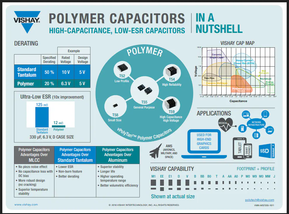
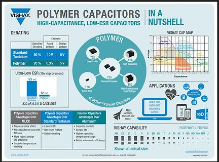
Vishay schickt eine Serie von Kondensatoren ins Rennen, die das Ziel hat, Tantal-Kondensatoren im High End-Bereich das Leben zu erschweren. Von Seiten des PR-Teams gibt es dabei die gezeigte Grafik, die die Vorteile gegenüber gewöhnlichen Tantal-Kondensatoren hervorhebt. , you can play for a longer time. This superior playback functionality, combined with a low power high performance U8 core,3V/5V compatible power supply and broad peripheral control functions, provide a single-chip solution for both battery- and AC-driven products. [/c] Der „Rest vom Schützenfest
VISHAY POLYMER CAPACITORS IN A NUTSHELL HIGH-CAPACITANCE, LOW-ESR CAPACITORS DERATING Example Specified Rated Design Voltage Standard Tantalum 50% 10V 5V Polymer 20% 6.3V 5V Ultra-Low ESR (10x improvement) 125 mΩ 12 mΩ Standard Tantalum Polymer 330 µF, 6.3 V, D CASE SIZE T52 Low Profile T54 High Reliability T55 General Purpose T59 High Capacitance High Voltage VPolyTan™ Polymer Capacitors VISHAY CAP MAP Ceramic Single Layer Heavy Current Polymer (ESR) Thin Film Aluminum Electrolytic
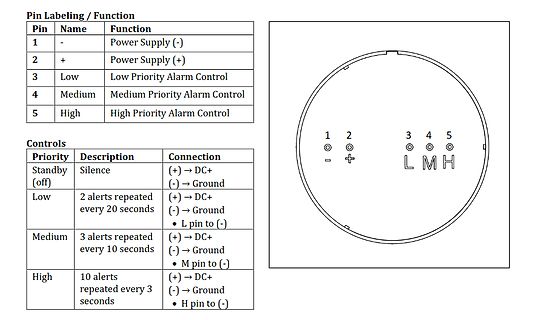
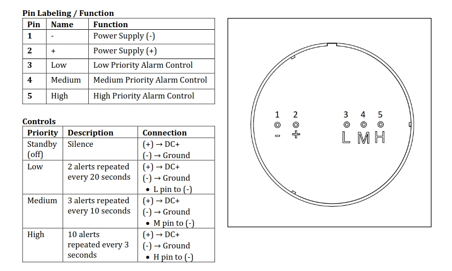
Pin Labeling / Function
Pin Name Function
1 - Power Supply (-)
2 + Power Supply (+)
3 Low Low Priority Alarm Control
4 Medium Medium Priority Alarm Control
5 High High Priority Alarm Control
Controls
Priority Description Connection
Standby (off) Silence (+) -> DC+
(-) -> Ground
Low 2 alerts

 Bild
Bild
 Bild
Bild
 Bild
Bild
 Bild
Bild
 Bild
Bild
 Bild
Bild