NOTICE. THE PRODUCTS DESCRIBED HEREIN AND THIS DOCUMENT ARE SUBJECT TO SPECIFIC DISCLAIMERS, SET FORTH AT www.vishay.com/doc?91000 OLED-128O032F-LPP3N00000 www.vishay.com Vishay MODULE CLASSIFICATION INFORMATION OLED - 128 O 032 F - L P P 3 N 0 0 000 1 2 3 4 5 6 7 8 9 10 11 12 13 1 Brand Vishay Intertechnology
inputs. H A variable gain control input which linearly adjusts the overall gain. The gain is zero at –1 V and maximum at +1 V. H Three separate differential outputs that can be turned on or off using the output enable control signals (out1en, out2en, out3en). The inv controls are left at 0. Table 1–
entspricht AVR Simulator 2 in 4.19), somit kann man ältere, aber noch immer aktuelle Mikrocontroller wie AT90CAN128 u.Ä. nur mit Studio 4 simulieren. P.S. statt WinAVR Version 20100110 benutze ich "per Hand" aus Atmel Studio herausgenommene spätere GNU Compiler-Version. Das bringt einige Vorteile, z.B.
4.19 ist auf eine ganz andere Generation Rechner optimiert. Wenn du wirklich noch einen Pentium 3, 128Mbyte RAM und einen Röhrenmonitor mit 1024 Pixel Horizontalauflösung nutzt, bleibe bei deiner Version.
, and the system clock can be divided by set- ting the “Clock Prescale Register – CLKPR” on page 35. This feature can be used to decrease 34 AT90USB82/162 7707F–AVR–11/10 AT90USB82/162 the system clock frequency and the power
Return flow safety device If the liquid levels in the circulator bath and the external system are at different heights, overflowing must be prevented after the power has been turned off. Flood hazard! For this reason, solenoid valves for loop circuit or shut-off valves can be integrated in the loop
Microcontroller Assembler and C High-level Language Code STK500 Top-Module Design 260 Bytes Code Size/128 Bytes Constants Table Size Use of Lookup Tables Application Note Introduction This application note describes how DTMF (Dual-Tone Multiple Frequencies) signal- ing can be implemented using any AVR microcontroller
etwas schwieriger zu löten, geht aber auch... Diese zwei Typen würde ich für alles empfehlen. Für CAN noch AT90CAN128, aber man kann auch ohne, mit einem externen CAN-Controller alles machen. Aber 8-Füßler - wozu?
Guide Section 3.1 // Addresses defined as offsets from the base address called RAM_REG and located at 0x302000 // Discussion: Defining this way leads to an additional add operation in code that can be avoided by defining // these addresses as 32 bit values, but this is easily paid for in clarity and
measure the frequency of a rectangular signal using an Atmega328P microcontroller in C programming, you can utilize one of the hardware timers available on the chip. The frequency measurement can be done by counting the number of rising or falling edges of the signal within a specific time period. Since
und Dein RAM hat. Wenn Du das Buffering der Lib reduzierst und statt ... [code] U8G2_SSD1309_128X64_NONAME0_F_4W_HW_SPI u8g2(U8G2_R0, 10, 9, 7); [/code] ... das hier nimmst: [code] U8G2_SSD1309_128X64_NONAME0_1_4W_HW_SPI u8g2(U8G2_R0, 10, 9, 7); [/code] ... so entspannt sich die
Guide Section 3.1 // Addresses defined as offsets from the base address called RAM_REG and located at 0x302000 // Discussion: Defining this way leads to an additional add operation in code that can be avoided by defining // these addresses as 32 bit values, but this is easily paid for in clarity and
transactions, the host sends a ‘0’ bit and ‘1rdbit, followed by the 6-bit command code. The 2 byte can be either 00h, or the parameter of that commandbyte is fixed at 00h. All SPI commands except the system reset can only be executed when the SPI is in the Single channel mode. They will be ignored when
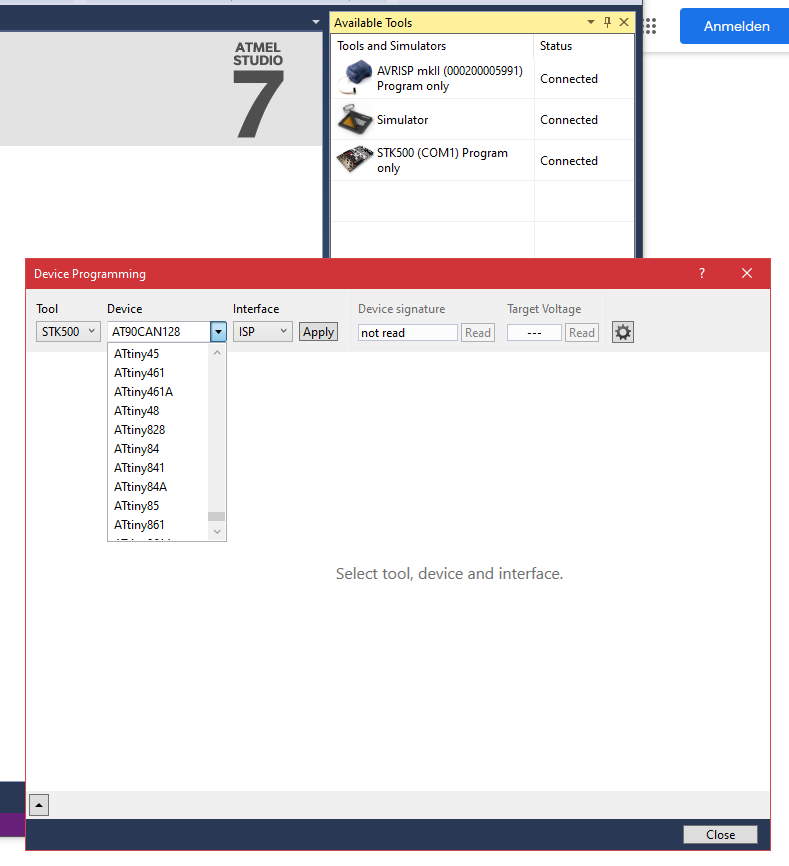
0,5 mm Pinabstand, aber notfalls geht das auch... Und meine Lieblinge ATMega1284(P) und auch AT90CAN128 kann ich wie früher mit Atmel AVR JTAGICE mkII bedienen: entweder aus Win11 über USB/RS232 Converter oder aus Win7 über USB mit dem älteren Notebook, da ich AVR Studio 4.19 einfach mag.
> 0,5 mm Pinabstand, aber notfalls geht das auch... Und meine Lieblinge > ATMega1284(P) und auch AT90CAN128 kann ich wie früher mit Atmel AVR > JTAGICE mkII bedienen: entweder aus Win11 über USB/RS232 Converter oder > aus Win7 über USB mit dem älteren Notebook, da ich AVR Studio 4.19 > einfach mag
washing process; in this case the requirements 1 with respect to clearances and creepage distances can change. curve 3: maximum voltage at contact current = 0 A curve 4: limiting voltage U 2 at rated contact current Irated recommended voltage range (shaded area): RT IV: sealed relay the coil voltage
after entering fast decay mode, until the blanking time has expired. To provide better current control at very low current steps, an adaptive blanking time mode can be enabled by setting the ABT bit in the BLANK register. If ABT is set, at current levels below 30% of full scale current (as determined by
and button for 3 seconds: MENU, Button the message “CONTROLS LOCKED” appears. CONTROLS LOCKED You can unlock the OSD controls at any time by pushing the MENU, button for 3 seconds: the message “CONTROLS UNLOCKED” will appear. CONTROLS UNLOCKED Headphone jack that automatically mutes the speaker volume
abnormality has occurred the unit, the protection circuit operates and reset to the stand by mode. At this time, the defective block can be identified by the number of blinks of the Power LED on the front panel of the unit. 19 7.3. No Power First check point There are following 3 states of No Power indication
F (10° to 35° C)* Non-operating: -22° to 140° F(-30° to 60° C) Relative Humidity Operating: 10% to 90% (non-condensing at ambient) Non-operating: 5% to 95% (non-condensing at ambient) (unpressurized) Operating: 10,000 ft (3048 m) Maximum Altitude Non-operating: 30,000 ft (9144 m) *NOTE: Operating temperature
F (10° to 35° C)* Non-operating: -22° to 140° F(-30° to 60° C) Relative Humidity Operating: 10% to 90% (non-condensing at ambient) Non-operating: 5% to 95% (non-condensing at ambient) (unpressurized) Operating: 10,000 ft (3048 m) Maximum Altitude Non-operating: 30,000 ft (9144 m) *NOTE: Operating temperature
that should be preserved across calls. In other words, when the caller makes a procedure call, it can expect that those registers will hold the same value after the callee returns. Thus, making it the callee's responsibility to both save (push at the beginning) and restore (pop accordingly) them before
more V R CENTER ....................................................................................90 W X SURROUND L/R ...........................................................90 W + 90 Wal Noise (IHF-A Network) R SURROUND BACK L/R ................................................90 W + 90 W FRONT L
a full-color version. There are 3 separate LED paths available for each monochrome backlight that can be switched in parallel or in series to suit the system voltage.This means that most backlights can be run at either 3.3V or 5 V. To operate the backlight, we recommend a current source (e.g. CAT4238TD
Burn-O-Mat configuration file Copyright (C) 2007 Torsten Brischalle This program is free software: you can redistribute it and/or modify it under the terms of the GNU General Public License as published by the Free Software Foundation, either version 3 of the License, or (at your option) any later version
these resistor values can range from 10 k to 30 k . 7. The pull-up or pull-down on this signal is only enabled at boot/reset for strapping function. 8. Simulation data shows that these resistor values can range from 10 k to
nonvolatile SPB. Both DPB and SPB states must be cleared to 00h before the associated sector or block can be modified. The SPB are preset to 00h at the factory and there is no need to modify them if you are only migrating from an E version product to the MX25L12835F. Please refer to the MX25L12835F datasheet
and data shifts out on the falling edge of SCLK at a maximum frequency fR. The first address byte can be at any location. The address is automatically increased to the next higher address after each byte data is shifted out, so the whole memory can be
frequency fC. The first address byte can be at any location. The address is automatically increased to the next higher address after each byte data is shifted out, so the whole memory can be read out at a single FAST_READ instruction. The
out. The address is latched on rising edge of SCLK, and data shifts out on the falling edge of SCLK at a maximum frequency fR. The first address byte can be at any location. The ad- dress is automatically increased to the next higher address after each byte data is shifted out, so the whole memory can
and data shifts out on the falling edge of SCLK at a maximum frequency fR. The first address byte can be at any location. The address is automatically increased to the next higher address after each byte data is shifted out, so the whole memory can be
that are contained in the terms of use for the Microsoft website that hosts this documentation, you can make copies of it in order to develop implementations of the technologies that are described in this documentation and can distribute portions of it in your implementations that use these technologies
to a 100V step. Dielectric ) 200 Sample C ( VDS= 0V n 100V i r Step Input C 100 VOUT= 1/C ∫ idt g 90 OPA k 80 L 70 t 60 G Thermal and STANDARD DIELECTRIC-EVALUATION SCHEMES can prove disas- Noise Threshold trous to the op amp they employ. If the dielectric under test shorts, the 10 resulting high voltage
the battery, and therefore provides accurate data about the remaining battery capacity. This data can be read through I2C from the PXA320 processor, or from any device on the extension board. The battery is charged whenever DC power is applied. DC power can be applied and removed at any time, also during
der AT90CAN128. Das Webgedöns programmieren andere, das ist mir zu öde. Ich mag es lieber hardwarenah.
zuverlässig startet. Da mußte man noch mit einem Supervisory-IC (MAX690) nachhelfen. Ich hatte mal beim AT90S2313 die FSTRT-Fuse gesetzt mit dem Erfolg, daß nach dem kurzen Delay der Quarz noch nicht angeschwungen war. Der AT90S2313 machte daher nichts beim Einschalten.
after entering fast decay mode, until the blanking time has expired. To provide better current control at very low current steps, an adaptive blanking time mode can be enabled by setting the ABT bit in the BLANK register. If ABT is set, at current levels below 30% of full scale current (as determined by
warning emitted [/code] [code] >file qaxe-rev2.bin qaxe-rev2.bin: ARM Cortex-M firmware, initial SP at 0x20004000, reset at 0x080000f4, NMI at 0x08009ece, HardFault at 0x0800c9d6, SVCall at 0x08009ece, PendSV at 0x08009ece [/code] [Mod: Code-Tags eingefügt]
es der 151C8. file qaxe-fw-L151C8.bin qaxe-fw-L151C8.bin: ARM Cortex-M firmware, initial SP at 0x20004000, reset at 0x080000f4, NMI at 0x0800a2a0, HardFault at 0x0800cdaa, SVCall at 0x0800a2a0, PendSV at 0x0800a2a0
shape Number of shocks: 3 shocks in 3 mutually perpendicular axes. Note 1: Product cannot sustain at extreme storage conditions for long time. Data Modul AG - www.data-modul.com 9 5. Electrical Specifications 5.1 Typical Electrical Characteristics At Ta = 25 °C, VDD = 3.3V±5%, VSS=0V. Table 5 Parameter
mit dem MSE abgetippt haben. Um das (potentielle) Rätsel noch zu erhöhen, könntest du das ganze AES 128 verschlüsseln. Evtl. kann man dies bis dahin knacken...
alt bist. Darunter wird der THC-Gehalt auf 10% gedeckelt. ;-) So steht es zumindest im kommenden CanG.
application must perform during mapping. Function 17 lets a program map (or unmap) multiple pages at one time. In addition, you can map pages using segment addresses instead of physical pages. For example, if the page frame base address is set to D000, you can map to either physical page 0 or segment
S 3 20-nov-04 20-feb-05 None noted Supply possible. Caen fire part. 278 TDA8708AT/C1 TDA8708AT D CONVERTERS (CAEN) 935063030112 T S 3 20-nov-04 20-feb-05 None noted Supply possible. Caen fire part. 279 TDA8708AT/C1 TDA8708AT D CONVERTERS (CAEN) 935063030118 T S 3 20-nov-04 20-feb-05 None noted Supply possible. Caen fire part. 280 TDA8709AT/C2 TDA8709AT D CONVERTERS (CAEN) 935075380112 T S 3 20-nov-04 20-feb-05 None noted Supply possible. Caen fire part. 281 TDA8709AT/C2 TDA8709AT D CONVERTERS (CAEN) 935075380118
at maximal battery voltage ηnom,V 90.64% batt,max 66 5.5 Selection of the Submodule’s Topology 5.5 Selection of the Submodule’s Topology The CHB inverter consists of several submodules connected in series
of this data sheet, please register at our Worldwide Web site at: http://www.microchip.com You can determine the version of a data sheet by examining its literature number found on the bottom outside corner of any page. The last character
frequency division is 12M. [3](Note: PLL input clock range is 12M*(1±35%), i.e. about 8M~16M, users can adjust the input frequency :appropriately to meet the needs of PLL output special frequency)up to 144M, different microcontroller families operate at different frequ nci s, with the STC32G12K128 family
schonmal ein anderer Controller ist. Welchen Bootloader hast du? Selber Programmiert? Ist der CAN im Controller oder über RS232 auf CAN? Wenn du einen bootloader suchst, probiere den mal, vieleicht hilft es dir weiter: https://github.com/JChristensen/mighty-1284p/tree/v1.6.3 Hier auch
die config ist nur gleich wie in der Firmware. Hab den fehler gefunden, es ist in der Config vom CAN-Controller bei der Initialisierung über den 64k Falsh - sowas musste es ja sein. Jetzt passt er leider mit 1032 Bytes nicht mehr in die Handlichen 512 Wörtern. Bei einen 128k MCU sollte aber 1024 Wörter
Enable. 3 Internal use, do not overwrite. 2:1 Subtractive Decode — These bits determine the point at which the PC87200 accepts cycles that are not claimed by another device. The PC87200 defaults to taking subtractive decode cycles in the default cycle clock, but can be moved up to the Slow Decode cycle

 Bild
Bild