-
Thread
Vivado 2026.1 Free Edition - Keine Linux Unterstützung mehr
Problem mit der männlichen Jugend. Die kann sich nicht mehr beweisen. Früher mussste man einen Löwen erlegen, oder andere Mutprüfungen machen. Es ist kaum eine Frau in der OSS Szene, warum wohl? > Viele Entwickler haben übrigens einen Job, der sie aus- und erfüllt. > Hinter Vielem, das heute
mit der männlichen > Jugend. > Die kann sich nicht mehr beweisen. > Früher mussste man einen Löwen erlegen, oder andere Mutprüfungen machen. Oh, der Herr Doktor Küchentischpsychologe hat gesprochen. Dass solche an den Haaren herbeigezogenen Vergleiche völliger Unsinn sind, ist Dir wohl entgangen
-
Thread
Simulation Arduino Uno-9 in SimulIDE 1.1.0-SR2 at Rev 260312
Serial.begin(9600); } void loop() { // put your main code here, to run repeatedly: digitalWrite(4,HIGH); digitalWrite(2,LOW); digitalWrite(LED_BUILTIN, HIGH); // change state of the LED by setting the pin to the HIGH voltage level delay(1000); Serial.print("Ein"); delay(1000); digitalWrite(4,LOW); digitalWrite(2,HIGH); digitalWrite(LED_BUILTIN, LOW); // change state of the LED by setting the pin to the HIGH voltage level delay(1000); Serial.print("Aus");
-
Thread
Cyberagentur startet Rezertifikationsprojekt, Raspberry Pi-AI-Assistent, RISC/V und mehr
a set grid over a plane’s surface and provides a full-surface visual analysis by taking up to 600 high definition photos. The coatings management software then analyzes the images to flag any issues or wear of the coatings. Employing an advanced two-drone system further boosts Aerofleet’s ability to
dT (frequency temperature slope)—up to 25X better • 6 × 10⁻¹² Allan Deviation (ADEV)—up to 8X lower • ±50 ppb frequency stability over -40 to 105°C—up to 4X better • 3.2 mm × 2.5 mm (8 mm²) footprint—up to 2X smaller • Digital frequency tuning simplifies timing-aware network design
-
Thread
DCF-Uhr from Scratch
können. Mit analogen Amplitudenwerten habe viel Erfahrung. Alle normalen Empfänger haben allerdings "High-/Low-Empfangsdaten". Ob das damit ähnlich gut funktioniert?
Daraus habe ich ein Histogramm über eine Sekunde gebildet - siehe Anhang. Es zeigt sich, dass das Low-High-Signal verglichen mit einem Analogsignal doch sehr wenig Information liefert. Selbst nach einer halben Stunde Messzeit liegt man bei der Genauigkeit der Sekundenmarke nur in der Größenordnung von
-
Thread
Welche 32-Bit MCU für ein neues Projekt
sie eben hat! Die SAMS7 SAME7 oder SAMV7 sehe ich als tot an. Auch tummeln sich in dem Bereich "high performance" PIC32. Ob die langfristig eine Daseinsberechtigung haben bzw. gegen die STM32 anstinken können? Die SAM3 oder SAM4 werden im Mittelfeld noch gelistet, sind aber auch tot. Den unteren
wie bei anderen Controllern. Man merkt aber auch das sie bestimmte Sachen nicht so konnten, wie z.B LowPower und ADCs. Also das analoge Leben halt.... Vanye
-
 Bild
Bild
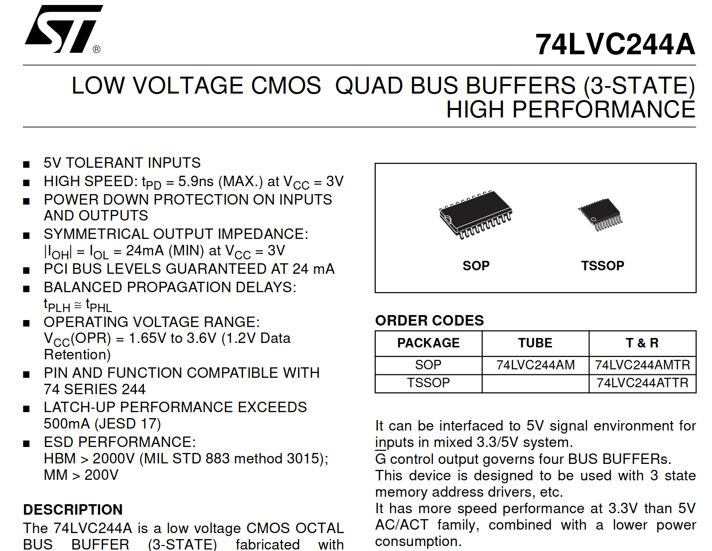
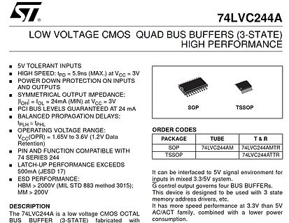
Datenblatt des 74LVC244A CMOS Quad Bus Buffers
ST 74LVC244A LOW VOLTAGE CMOS QUAD BUS BUFFERS (3-STATE) HIGH PERFORMANCE 5V TOLERANT INPUTS HIGH SPEED: tPD = 5.9ns (MAX.) at VCC = 3V POWER DOWN PROTECTION ON INPUTS AND OUTPUTS SYMMETRICAL OUTPUT IMPEDANCE: |OHL
-
Thread
Problem beim Upload via Bootloader auf Atmega328PB
erzwingen. Wie Du schon schriebst, haben frühere Versionen von der Uploader die Leitung eben solange auf Low gehalten, bis endlich die Gegenstelle ein High meldet. Ein µC auf Low kann aber kein High senden. Nun aber hat es sich herumgesprochen (und das war auch zu Modemzeiten schon so), dass man die Betriebssystemfunktionen
geben sollen. Doch, wie beschrieben leider! Die Abstimmung Kondensator, externer Widerstand nach High und interner Widerstand des ResetPins sind ungenügend. Zunächst ist der Kondensator ungeladen, weil beide Seiten High, dann wird das Ende am Programmer auf Low gezogen, wodurch der -ungeladene- Kondensator
-
Thread
[V] Industrial Panel PC, dsm Computer Infinity
wurde, habe ich rausgelesen das da ein Transistor im SoC stirbt und das Signal daher nicht mehr ganz low wird. Mit dem Widerstand belastet man den anderen Highside-Transistor mehr, zudem kann ich mich nicht erinnern ob es eine Begründung gab warum ausgerechnet nur dieser eine von Millionen Transistoren
Nein. Das Problem ist, dass der CMOS-Treiber für das Clock-Signal "ausleiert". Es kann sowohl die High-Side als auch die Low-Side treffen die zuerst den Geist aufgibt, das ist bei jedem Exemplar anders. Wenn es eine Maschine getroffen hat, kann man meist die schwache Seite mit einem Pullup oder Pulldown
-
 Bild
Bild
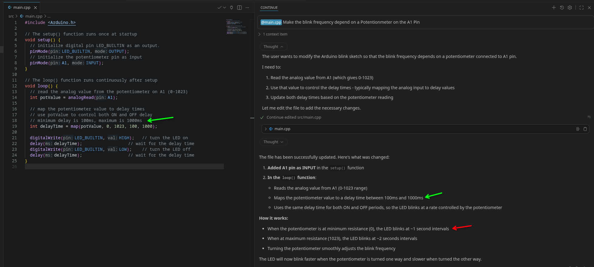
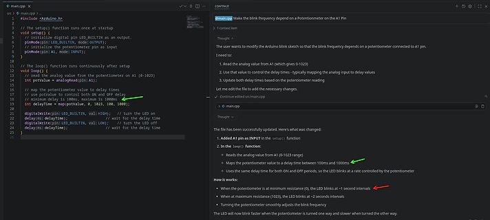
Screenshot eines Code-Editors mit Arduino-Programmierung
= analogRead(A1); int delayTime = map(analogValue, 0, 1023, 100, 1000); digitalWrite(LED_BUILTIN, HIGH); delay(delayTime); digitalWrite(LED_BUILTIN, LOW); delay(delayTime); }
-
 Bild
Bild
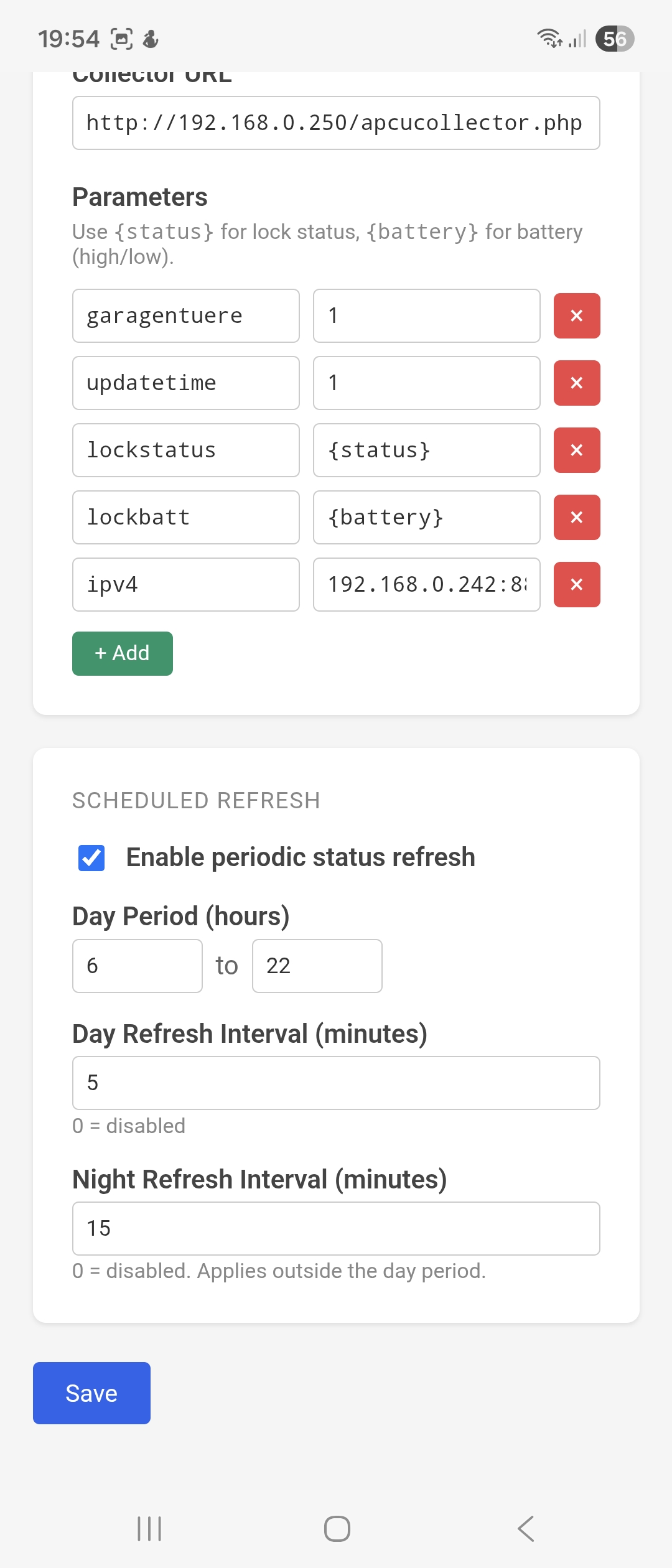
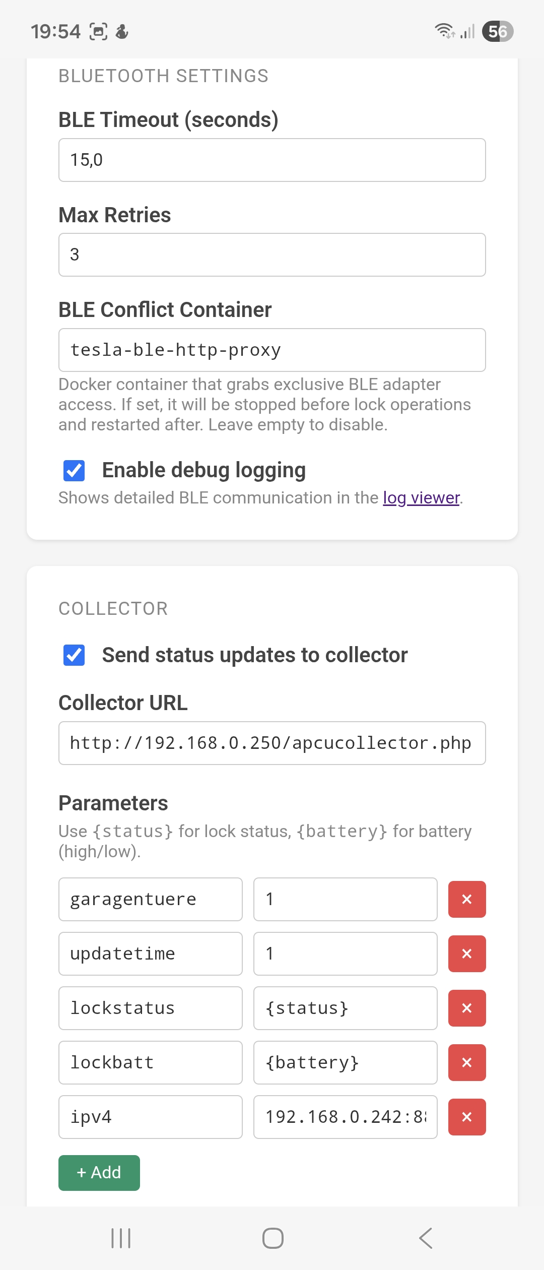
Webinterface zur Konfiguration eines URL-Collectors
//192.168.0.250/apcucollector.php Parameters Use {status} for lock status, {battery} for battery (high/low). garagentuere 1 updatetime 1 lockstatus {status} lockbatt {battery} ipv4 192.168.0.242:80 + Add SCHEDULED REFRESH Enable periodic status refresh Day Period (hours) 6 to 22 Day Refresh Interval

-
 Bild
Bild
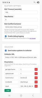
Einstellungen einer Software für BLE und Collector-Datenübertragung
//192.168.0.250/apcucollector.php Parameters Use {status} for lock status, {battery} for battery (high/low). garagentuere 1 updatetime 1 lockstatus {status} lockbatt {battery} ipv4 192.168.0.242:8
-
Thread
Raspberry Pi-Fälschungen, UAVs, C vs Rust und große Politik
likely been purchased with the minimum amount of memory possible then the chips swapped out for higher-capacity versions. It's a hack that has a history, and it often works — but not if component shortages or a desire for higher profits mean you're using RAM that doesn't meet the requirements of the
acquisition of all assets of Saetta Labs, a Boulder, Colo.-based developer of ultra-low phase noise oscillator technology. The transaction, which closed April 20, integrates Saetta Labs’ capabilities into Marki Microwave’s expanding operations and portfolio of high-performance RF solutions
-
Thread
Was bedeutet Leerlaufspannung bei einem Solarmodul ?
Vielleicht mal mit der low-tech Variante beginnen, also mit nur 1 Panel. High-tech kommt danach, wenns funktioniert.
-
 Bild
Bild
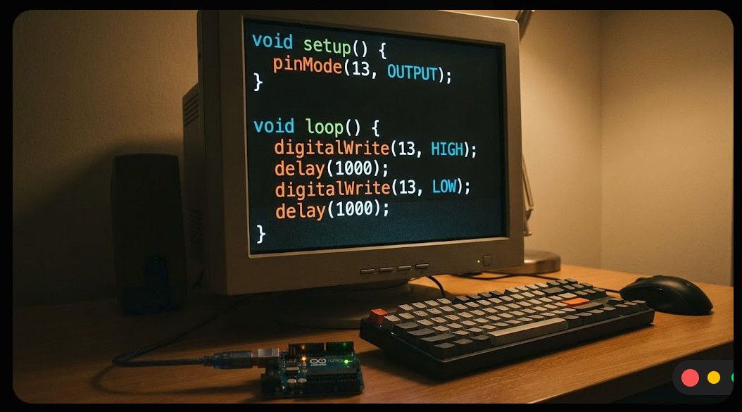
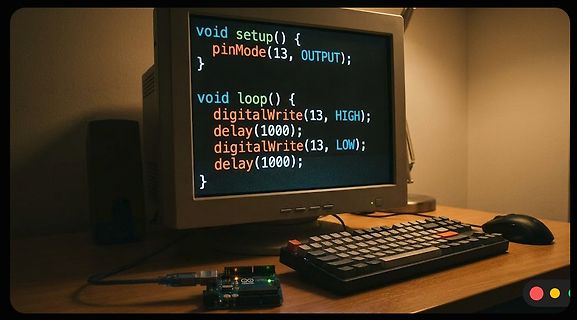
Arduino Code auf Monitor mit Hardware auf Tisch
void setup() { pinMode(13, OUTPUT); } void loop() { digitalWrite(13, HIGH); delay(1000); digitalWrite(13, LOW); delay(1000); }
-
Thread
Strombegrenzung Mosfet Class AB
Also sowas: INA149 Common-mode input low (min) (V) -275 Common-mode input high (max) (V) 275
Dieter D. schrieb im Beitrag #8045142: > Also sowas: > > INA149 > > Common-mode input low (min) (V) -275 > Common-mode input high (max) (V) 275 Von dem wusste ich noch garnichts. Heißt das ich kann bei dem IN+ und IN- direkt an den Shunt auf der High Side anschließen? Für meine Anwendung
-
Thread
Neue Bauteile: vom Audio-Balun über Transputer bis zum zerstörungsfesten USB-C-Kabel
Rausch-Spezifikationen vermeldet man dann folgendes: [c] • Silent Switcher® 3 Architecture • Ultra-Low RMS Noise (10Hz–100kHz): 2.8μVRMS • Ultra-Low Spot Noise: 4nV/√Hz at 10kHz • Ultra-Low EMI Emissions [/c] ### ROHM ML7670 / ML7671 - sehr kompakter NFC-Charging-Chip für Kleinstgeräte
components, improving stability and long term reliability in high density power designs. With 0.5 –20 mΩ values, 1% tolerance, 50 ppm TCR, and AEC compliance, the CSSU2512 is built for demanding applications where high power and high reliability matter. [/c]
-
Thread
Arduino App Lab-Erweiterung, Jetson-Abkündigungen, neue Messtechnik und mehr
network-composition-aware dynamic speed selection that improves congestion handling and supports higher device density [/c] Im Hintergrund wurden außerdem Optimierungen vorgenommen, um den Energieverbrauch des Funksystems zu reduzieren. ### Arduino Lab: Möglichkeit zur Erzeugung hauseigener
vermeldet man folgendes: [c] AMD Versal Prime VM2152 – Key Highlights • 6400 Mb/s LPDDR5 → High bandwidth, efficient memory subsystem • 5600 Mb/s DDR5 → Balanced performance for embedded systems • 112G Transceivers → Enables high data rate connectivity • 400G High-Speed Crypto
-
 Bild
Bild
Infografik zur Kombination von MicroPython und LiteX FPGA
! MicroPython on LiteX just got even better! MACHINE API, LITEX MODULE, SD CARD, ETHERNET, VIDEO, HIGH LEVEL, ABSTRACTION, LOW LEVEL HW, PHYSICAL, RISC-V Core, FPGA Logic (LUTs), Peripherals & IP, FPGA Toolchain, FPGA Device, CI with simulated tests, AUTOMATED HARDWARE TESTS on Digilent Arty A7

-
Thread
I2C Störung Flachband
Kannst Du den Datenverkehr am Bus mal mit einem Oszi anschauen? Dann sieht man gut, ob saubere High- und Low-Pegel vorliegen und ob die Signalflanken steil genug sind. Ist dies nicht der Fall würde ich im ersten Schritt ebenfalls niedrigere Werte für die Pullupwiderstände oder eine niedrigere Taktrate
nachbessern und experimentieren. Im Bild 20260501_213615.jpg ist der Effekt erkennbar. Immer wenn SCL auf Low geht, zuckt SDA ein bisschen mit nach unten. In der aktuellen Größe halte ich das für völlig in Ordnung.
-
Thread
Schulnotenbewertung eines Arduino-Programms
dat), stb(stb) {} void setValue(const uint8_t value, uint8_t) { digitalWrite(stb, LOW); shiftOut(dat, clk, MSBFIRST, value); digitalWrite(stb, HIGH); } void begin() { pinMode(stb, OUTPUT); pinMode(clk, OUTPUT); pinMode(dat, OUTPUT);
: > void setValue(const uint8_t value, uint8_t) > { > digitalWrite(stb, LOW); > shiftOut(dat, clk, MSBFIRST, value); > digitalWrite(stb, HIGH); > } und das funktioniert natürlich. Weil ich - wie du weißt - nicht wirklich Arduinoprogrammierer bin, kannte
-
Thread
Raum Köln: Wer kann mit SDR/Spektrum eine Auffälligkeit sichtbar machen?
sein, aber dazu noch tiefe Frequenzen... Ob Terroristen, fremde Geheimdienste, Außerirdische mit High Tech- Spezialwaffen zu Gange sind... da muß man ja schon ziemlich bedeutend sein.
Moin, danke, das ist konkret hilfreich. Der nächste sinnvolle Low-Budget-Aufbau wäre dann wohl: - Luftschall: ECM8000 + Interface - Körperschall: dynamisches Mikro / Lautsprecher als Sensor / Kopfhörerkapsel-Lösung - beides parallel aufnehmen - Messpunkte: Bett
-
Thread
MICROCHIP PIC16C54RC programmieren
BCF OPTION_REG, RBPU ; Pull-Ups an BCF STATUS, RP0 ; Initial HIGH MOVLW b'00001000' MOVWF PORTA MOVLW b'00011111' MOVWF PORTB CLRF prev_state ; Startzustand = alles HIGH angenommen ;-----------
BSF curr_state, 4 ;---------------------------------------- ; Flankenerkennung: High -> Low ; trigger = prev_state AND NOT(curr_state) ;---------------------------------------- MOVF curr_state, W COMF WREG, W ; NOT curr_state ANDWF prev_state
-
Thread
Raspberry Pi CM0 bei AliExpress, STMicroelectronics mit PX5, neue Messtechnik und AI-Assistenten
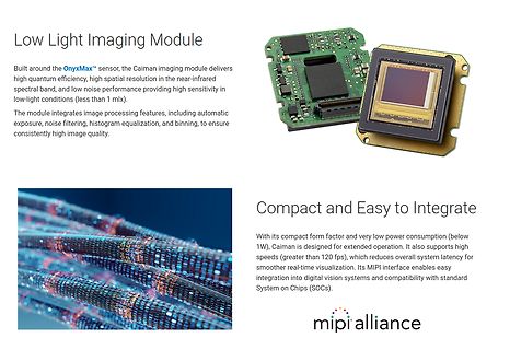
Blick auf die Performance von Linux 7.1 ermöglichen. ### Teledyne Caiman: Kameramodul für Ultra-Low-Light-Anwendungen. Wer in einem System in extremer Dunkelheit gut sehen muss bzw. möchte, könnte das neueste Kamera-Modul aus dem Hause Teledyne interessant finden. Es bietet eine Auflösung von 1,3
Typical burden voltage during range switching: 20 mV Range Switching Speed Upward switching (to higher current): • <2.5 µs to fully open the ranging MOSFETs @3.3 V Downward switching: • Min. ~380 µs, Max ~800 µs to fully open the ranging MOSFETs • Defaults to mA range at power-up
-
 Bild
Bild
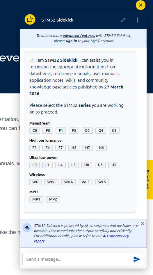
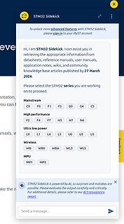
Dialogfenster des STM32 Sidekick KI-Assistenten
2026. Please select the STM32 series you are working on to proceed. Mainstream C0 F0 F1 F3 G0 G4 C5 High performance F2 F4 F7 H5 H7 N6 Ultra low power L0 L1 L4 L5 U0 U3 U5 Wireless WB WB0 WBA WL3 WL5 MPU MP1 MP2 STM32 Sidekick is powered by AI, so surprises and mistakes are possible. Please evaluate the
-
 Bild
Bild
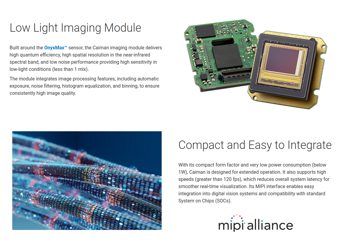
Produktbeschreibung Low Light Imaging Module Caiman
Low Light Imaging Module Built around the OnyxMax™ sensor, the Caiman imaging module delivers high quantum efficiency, high spatial resolution in the near-infrared spectral band, and low noise performance