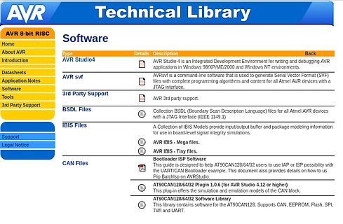
3rd Party Support
Support
Legal Notice
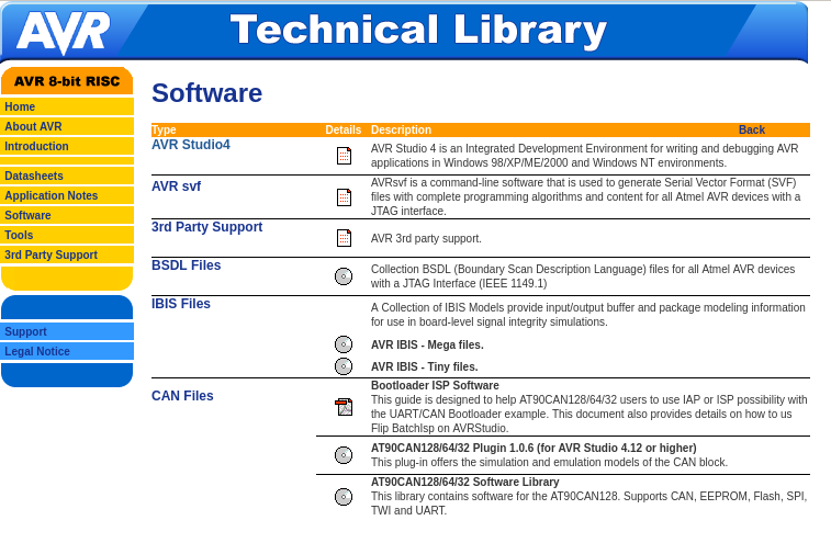
AVR Studio4
AVR svf
3rd Party Support
BSDL Files
iBIS Files
CAN Files
AVR 3rd party support.
Collection BSDL files for all Atmel AVR devices with a JTAG interface (IEEE 1149.1)
A Collection of IBIS Models
AVR IBIS - Mega files.
AVR IBIS - Tiny files.
Bootloader ISP Software
AT90CAN128/64/32 Software Library
connects the pin to the VIO voltage. Open-drain outputs are typically used when interfacing to logic at a higher voltage than the VIO pin. These pins can be safely pulled to the higher, external voltage through an external pull-up resistor. The maximum external pull-up voltage is 5 V. The speed of reading
clock frequency as described in the General Operating Ratings section. The system clock prescaler can be changed back after the oscillator calibration value has been updated. OSC20M Stored Frequency Error Compensation This oscillator can operate at multiple frequencies, selected by the value of the
Hallo, ich bin auf der Suche nach einer Fassung für den AT90CAN128. So, wie die hier https://www.reichelt.de/de/de/shop/produkt/ic-fassung_68-polig_plcc-14703 Allerdings in 64-polig. Bei meiner Suche finde ich nur 68-polig. Weiss jemand, wo ich die
Den AT90CAN128 gibt es auch im QFN-Gehäuse. Die sind deutlich stabiler, also müssten die Sockel eigentlich einfacher sein. Naja, Textool hat 2 verschiedene für 0.4mm-Pitch und scheinbar keinen für 0.5mm. Muss
possible performance. The the device is controlled by a separate logic input, DMOS output transistors can operate at supply while a common enable controls both channels. voltages up to 42V and efficiently at high switch- The I.C. is mounted in three different packages. BLOCK DIAGRAM July 1997 1/20 This
connects the pin to the VIO voltage. Open-drain outputs are typically used when interfacing to logic at a higher voltage than the VIO pin. These pins can be safely pulled to the higher, external voltage through an external pull-up resistor. The maximum external pull-up voltage is 5 V. The speed of reading
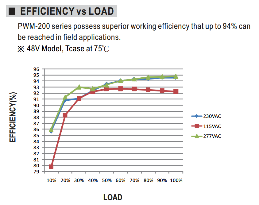
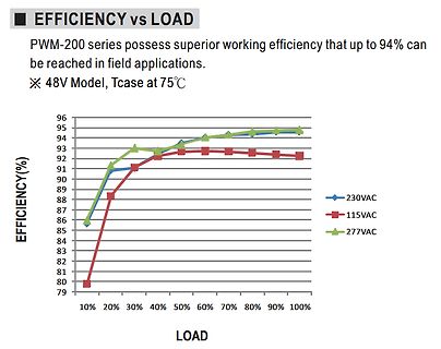
EFFICIENCY vs LOAD
PWM-200 series possess superior working efficiency that up to 94% can be reached in field applications.
※ 48V Model, Tcase at 75°C
EFFICIENCY(%)
LOAD
230VAC
115VAC
277VAC
10% 20% 30% 40% 50% 60% 70% 80% 90% 100%
CARD_POWER 1 G N D 20 FG1 DIR G LOW = Power OFF FG2 TC74VHCT245AFT SCAB1A8100 R255 1 IC94B 100k HD74LV32AT D IC90C IC90D RPC05T@J D 5 CARD_XBUSEN HD74LV00AT HD74LV00AT XCARD_BUS_ENABLE 6 RPC05T@J 9 12 XCA_IOIS16 4 R254 22 8 11 XIOIS16 10 13 RPC05T@J R256 NIU D +5 D +3.3 D LTLXBIG LTLXBIG R257 0 R258 NIU R259
5.9 13.0 9.0 7.7 15.0 13.8 11.2 15.0 15.0 13.7 (A) Peak Current (A) 63.5 30.1 24.9 89.0 44.9 37.0 90.0 64.0 54.1 90.0 73.7 58.9 Don’t see exactly what you need? Optional: Tachometer Specifications Still need help? Have ElectroCraft build you a Model Easily build your own motor at Tach Resistance Tach
Powering the Target These are configuration essentials: • When using the USB connection, PICkit 3 can be powered from the PC but it can only provide a limited amount of current, up to 30 mA, at VDD from 1.8-5V to a small target board. • The desired method is for the target to provide VDD since it can provide a higher current. The additional benefit is that plug-and-play target detection facility is inherited, i.e., MPLAB IDE will let you know in the Output window when it has detected the target
the forward converter works at the pre-regulated intermediate circuit voltage. This means that a higher transformer ratio can be selected, reducing the current load for the MOSFET. Furthermore, a larger duty cycle can be set during
/K ± 1.0 % UB C1 51R1 = 51.1 Ω MBE/SMA 0414 ± 2.0 % L0 RP ± 5.0 % KL R2 R4 N4 Notes • The products can be ordered using either the PRODUCT DESCRIPTION or the PART NUMBER. • Standard products are not CECC approved. • Radial version (RB,UB) cannot be qualified according to CECC so these can only be ordered
CARD_POWER G N D FG1 1 DIR G LOW = Power OFF 20 FG2 0 TC74VHCT245AFT SCAB1A8100 R255 1 IC94B 100k HD74LV32AT D IC90C IC90D RPC05T@J D 5 CARD_XBUSEN HD74LV00AT HD74LV00AT XCARD_BUS_ENABLE 6 RPC05T@J 9 12 XCA_IOIS16 4 R254 22 8 11 XIOIS16 10 13 RPC05T@J R256 NIU D +5 D +3.3 D LTLXBIG LTLXBIG R257 0 R258 NIU R259
addition, there is a user range. User write to the memory is restricted to the NVM User Range. User read can also be performed to the other NVM addresses. 4.8.1 NVM User Range The host can write and read the memory of the user range. The range is located at addresses 0x20-0x22. Each address holds 2 bytes.
is enabled with ACC_CONF.acc_perf_mode=0b1. In this power mode, the accelerometer data is sampled at equidistant points in the time, defined by the accelerometer output data rate parameter ACC_CONF.acc_odr. The output data rate can be configured in one of eight different valid ODR configurations going
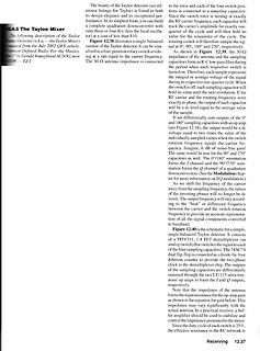
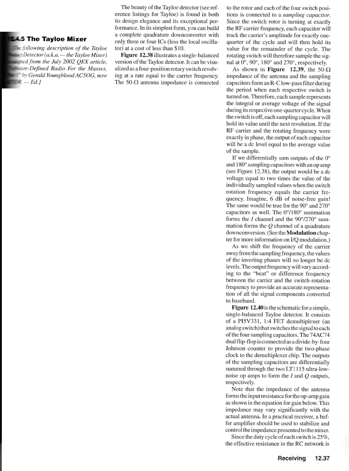
detector is for you, build its design elegance and its exceptional performance. In its simplest form, you can build a complete quadrature downconverter with only three or four ICs (the local oscillator, mixer, and amplifiers). Figure 12.38 illustrates a single-balanced version of the Tayloe detector. It can be visualized as a four-phase rotation switch revolving at a rate equal to the carrier frequency. The 50-Ω impedance of the antenna and the sampling capacitors form an R-C low-pass filter during the periods when the switch is turned on. Therefore, when the switch
inverting CMOS gate or combination of gates could be used. This means left over portions of gate packages can be often used. The duty cycle will be close to 50% and will oscillate at a frequency that is given by the fol- lowing expression. AN006022-2 FIGURE 2. Three Gate Oscillator Propagation Delay vs Ambient
This pin is Data/Command control pin connecting to the MCU. When the pin is pulled HIGH, the data at D[7:0] will be interpreted as data. When the pin is pulled LOW, the data at D[7:0] will be transferred to a command 12 D/C register. In I2C mode, this pin acts as SA0 for slave address selection. When
time, clock input pulse width and maximum frequency 9, &3▯LQSXW 90 *1' WVX VX W W 9 K K , 'Q▯LQSXW 90 *1' 92+ 4Q▯RXWSXW 90 9 2/ 92+ 4Q▯RXWSXW 90 92/ DDD▯▯▯▯▯▯▯ Measurement points are given in Table 8. Fig 8. Data set-up and hold times for data input 74HC_HCT175 All
expansion to a 1-of-32 (5 to 32 lines) decoder with just four '138 ICs and one inverter. The '138 can be used as an eight output demultiplexer by using one of the active LOW enable inputs as the data input and the remaining enable inputs as strobes. Inputs include clamp diodes. This enables the use
data (nD), clock (nCP), set (nSD) and reset (nRD) inputs, and complementary nQ and nQ outputs. Data at the nD-input, that meets the set-up and hold time requirements on the LOW-to-HIGH clock transition, is stored in the flip-flop and appears at the nQ output. Schmitt-trigger action in the clock input,
number of inputs switching; (CL VCC2 o ) = sum of outputs. 11. Waveforms 9, Q$▯▯Q%▯▯Q&▯LQSXW 90 *1' W W 3+/ 3/+ 92+ 9< Q<▯RXWSXW 90 9; 9 2/ W W 7+/ 7/+ ▯▯▯DDO▯▯▯ Measurement points are given in Table 8. VOLand V OHare typical voltage output levels that occur with the output load. Fig 6. Input to
Typ Max Min Max Min Max 74HC08 pd propagation nA, nB to nY; see Fig. 6 [1] delay VCC = 2.0 V - 25 90 - 115 - 135 ns V = 4.5 V - 9 18 - 23 - 27 ns CC VCC = 5.0 V; CL= 15 pF - 7 - - - - - ns VCC = 6.0 V - 7 15 - 20 - 23 ns t transition time see Fig. 6 [2] V = 2.0 V - 19 75 - 95 - 110 ns CC VCC = 4.5 V
Bin Category Min. Max. D 8.40 15.30 IV Bin Category Min. Max. E 12.60 23.10 Red IV Categories F 18.90 37.80 C 13.10 24.00 G 30.60 61.20 D 19.70 36.10 H 49.50 97.90 E 29.60 54.20 I 80.10 158.40 F 44.90 88.80 J 129.60 253.40 G 71.90 143.80 H 116.50 227.70 Yellow IV Categories Table 8: HLMP-2550/2855/2870
high- current drive capability for directly driving LEDs. Each 2 Applications quasi-bidirectional I/O can be used as an input or output without the use of a data-direction control • Telecom Shelters: Filter Units signal. At power on, the I/Os are high. In this mode, • Servers only a current source to V
6 7 8 9 1 2 3 SDA Data from transmitre Data from transmitre Transmitter must release the SDA line at this point, Receiver must release the SDA line allowing the Receiver to pull the SDA line low to at this point so the Transmitter can acknowledge the previous eight bits of data. continue sending data
response of the output PNP device can cause a turn-on delay giving crossover distortion on the negative going transition through zero crossing at the higher audio frequencies. THD + N: Total Harmonic Distortion plus Noise refers to the
see Figure 4) Delay response time V <4V, 1.5A<Iout<25A SENSE tDSENSE2H from rising edge of SENSE = 90% of SENSE max - 270 600 µs INPUT pin (see Figure 4) Delay response time VSENSE < 4V, Δt between rising edge of ISENSE = 90% of SENSEMAX, - - 280 µs DSENSE2H outputcurrentand risingIOUT = 90% of OUTMAX
housed in a the chip in harsh environments. standard SO-8 package. The OMNIFET II are Fault feedback can be detected by monitoring the designed in STMicroelectronics VIPower M0-3 voltage at the input pin. BLOCK DIAGRAM DRAIN1 DRAIN2 OVERVOLTAGE OVCLAMPTAGE CLAMP INPUT1 INPUT2 GATE GATE CONTROL CONTROL
V pulses 0.5 s 5 s 2 ms, 10 5000 2a +37 V +50 V pulses 0.2 s 5 s 50 s, 2 3a -100 V -150 V 1h 90 ms 100 ms 0.1 s, 50 3b +75 V +100 V 1h 90 ms 100 ms 0.1 s, 50 4 -6 V -7 V 1 pulse 100 ms, 0.01 5b(2) +65 V +87 V 1 pulse 400 ms, 2 (1) ISO 7637-2: Test level results 2004(E) Test pulse III IV
junction-ambient 521) 37(2) °C/W 1. to alCCpins. Horizontal mounting and no artificial air flow.cm of Cu (at least 35 µm thick) connected 2. all Vpins. Horizontal mounting and no artificial air flow.cm of Cu (at least 35 µm thick) connected to CC 2.3 Electrical characteristics ) t( s otherwise stated.in this
turn-off current versus load inductance ILMAX (A) 100 10 A B C 1 0,1 1 10 100 L(mH) A = single pulse at TJstart 150 °C B= repetitive pulse at Jstart 100 °C C= repetitive pulse at Jstart 125 °C Conditions: VCC = 13.5 V V INIL Demagnetization Demagnetization Demagnetization t Note: Values are generatedLwith
junction-ambient (max) 51.3 37 °C/W 2 1. When mounted on FR4 printed circuit board with 0.5 cm of Cu (at least 35 µm thick). 2. When mounted on FR4 printed circuit board with 6 cm of Cu (at least 35 µm thick). Doc ID 10896 Rev 4 7/27 Electrical specifications VN920SP-E 2.3 Electrical characteristics Values
Register are both 1. Changes to Status Register bits caused by a change of Tx or Rx operating mode can take up to 150s to take effect. In Rx modem modes b2-1 will be 0 and b0 will show the output of the frequency demodulator, updated at 8 times the nominal data rate. A B Rx DTMF bursts Status Register
16 When high, do not read data from the FIFO. When low, there is data available in the FIFO which can be read by driving RD# 26 RXF# OUTPUT low. When in synchronous mode, data is transferred on every clock that RXF# and RD# are both low. Note that the OE# pin must be driven low at least 1 clock period
loader then determines if the device should stay in bootload mode or jump to the reset vector located at 0x0000. When the bootloader is not present, the device will jump to the reset vector of 0x0000 after any reset. More information about the bootloader protocol and usage can be found in AN945: EFM8 Factory
& P3.7 test TWI ext.bypassed? bypassed? ROM ROM program Execution 0000h ACK? E2PROM at 01 Program is downloaded from External EEPROM into internal External E2PROM (at 01) is detected EEPROM and CRAM and executed. SSB & P3.6 test UART bypassed bypassed? U Character An ISP Software can be
Durchschnittsverbrauch der 10 größten Stromfresser: https://www.ikb.at/energie/energieberatung/energiespartipps/die-10-groessten-stromfresser-im-haushalt
Identischer Lichtstrom bei einem Zehntel der elektrischen Leistung. Anderes Beispiel: In den 90er Jahren tobte der Prozessorkrieg zwischen Intel und AMD. Rechenleistung war Trumpf. Der thermische Leistungsumsatz je Quadratzentimeter übertraf den einer elektrischen Kochplatte deutlich (!!)
schon gezogen. Der VTarget auch. Vermutlich kommt der ARef-Wert durch durch die ADC6 Verbindung zum AT90S8535?
Behauptungen. In einem anderen Forum behauptete mal jemand, dass das 2.0a-Update mit älteren Boards mit AT90S* nicht gehen soll. Passt aber nicht, meines gehört zu dieser Kategorie (ca. 2002 gekauft) und läuft schon ewig mit 2.0a.
3.3V to 5V CC — 34 60 TA= 25°C, IF= 0.5 mA, R L 4.7 kΩ 4701/4731 — — 90 F = 0.5 mA, RL= 4.7 kΩ 070A/073A — — 130 F = 0.5 mA, RL= 4.7 kΩ Common Mode Transient |CM H 1,000 10,000 — V/μs IF= 0 mA,R =L4.7to 11kΩ, 7 d, e Immunity at Logic High Output V = 10 V , T = 25°C CM p-p
see Fig.14) Resetting and reactivating the interrupt circuit is achieved A quasi-bidirectional I/O can be used as an input or output when data on the port is changed to the original setting or dataisreadfromorwrittentotheportwhichhasgenerated without the use of a control signal for data direction. At
73.2 22.1 5 - 22 2.2 22 - 68 5 124 22.1 5 - 22 3.3 22 - 68 (1) Optional For higher output voltages at or above 1.8 V, additional phase boost can be achieved by adding a feed forward capacitor (C4) in parallel with R1. Since the DC gain is dependent on the output voltage, the required inductor value will increase as the output voltage increases. For higher output voltages at or above 1.8 V, additional phase boost can be achieved by adding a feed forward capacitor (C4) in parallel with R1 The inductor peak-to-peak ripple current, peak current and RMS current are calculated
When connected to PDWN pin, this pin can be used for auto power up. Thispinpresentstheoutputofthedemodulatorwhenchipinpowerupmode.Thisdatastream DOUT O includes the alternate ²1² and ²0² pattern, the marking, and the data. At all other times
temperature of 150°C. Limitations The power averaged over a complete switching cycle for repetitive pulses at various case temperatures can be must be less than: determined by using the thermal response curves. ON T − T Semiconductor Application Note, AN569, “Transient J(max) C Thermal Resistance−General Data
beschrieben: [c] Due to the significant ML improvements in the Armv9 architecture, a quad-core Cortex-A320 can execute up to 256 GOPS, measured in 8-bit MACs/cycle when running at 2GHz. As a result, Cortex-A320 can run advanced ML and AI use-cases directly on the CPU, even without the need for an external accelerator
because (1) it has a 3-wire serial port built-in that is used to clone 2 calculators together, so I can use it to connect to the UART port on my Strong SRT 2023 Android board, previously flashed with Armbian + Ubuntu. I just had to solder the wires (send, receive, ground) and voila, I can easily exchange

 Bild
 Bild
 Bild