please see www.vishay.com/doc?99912 Note (1)AEC-Q200 qualified parts are available per tables “Temperature Coefficient and Resistance Range”. DESCRIPTION MBA/SMA 0204, MBB/SMA 0207, and MBE/SMA 0414 professional leaded thin film resistors are the general
None-volatile memory (NVM) T = 85°C, 10 y Data Retention after 15 cycles Mechanical Shock Duration ≤ 200µs 10,000 g Duration ≤ 1.0ms 2,000 g Free fall 1.8 m onto hard surfaces ESD, at any pin HBM 2 kV CDM 500 V MM 200 V Note: Stress above these limits may cause damage to the device. Exceeding the specified
Product complies to MSL Level 4 acc. to JEDEC J-STD-020E OHA04525 300 ˚C T 250 T 245˚C 240˚C p t 217˚C P 200 t L 150 S 100 50 25˚C 0 0 50 100 150 200 250 s 300 t Profile Feature Symbol Pb-Free (SnAgCu) Assembly Unit Minimum Recommendation Maximum Ramp-up rate to preheat *) 2 3 K/s 25 °C to 150 °C Time t t
listed in the figure, refer to the respective data sheet or contact your nearest Broadcom representative for details. 2. Bin options refer to shippable bins for a part number. Color and Intensity Bins are typically restricted to 1 bin per tube (exceptions may apply). Refer to respective data sheet for specific bin limit information. Broadcom AV02-4479EN 6 HLCP-A100/-B100/-C100/D100/-E100/-G100/-H100, HLMP-2300/-2350/-2400/ -2450/-2500/-2550, HLMP-2600/-2620/-2655/-2670
literature number SLUA271 (www.ti.com/lit/slua271). 5. Vias are optional depending on application, refer to device data sheet. If any vias are implemented, refer to their locations shown on this view. It is recommended that vias under paste be filled, plugged or tented. www.ti.com EXAMPLE STENCIL DESIGN
accommodate the shorter maximum permissible rise time for the Fast-mode I 2C-bus. For bus loads up to 200 pF, the pull-up device for each bus line can be a resistor; for bus loads between 200 pF and 400 pF, the pull-up device can be a current source (3 mA max.) or a switched resistor circuit (see Section
Cycles Note 1: 24XX256 is used in this document as a generic part number for the • Data Retention >200 years • Factory Programming Available 24AA256/24LC256/24FC256 devices. • RoHS Compliant • Temperature Ranges: - Industrial (I): -40C to +85C - Extended (E): -40C to +125C • Automotive AEC-Q100 Qualified
www.ti.com Typical Application *Optional components dependent upon specific design requirements. Refer to External Components Description for a component functional description. Figure 1. Typical Audio Amplifier Application Circuit Connection Diagram Top View Preliminary: call your local Texas Instruments
2C477&sr=8-1&th=1&linkCode=sl1&tag=shakeela65-21&linkId=6caee1a7cf14f17032b61a2820bbb3f2&language=de_DE&ref_=nav_signin Ich denke 250 € + Versand nach Wahl ist fair. Paypal oder Banküberweisung, wie gewünscht. Gruss Piefke
128GB SSD, Celeron 5205U, 15.6 HD Panel, 4GB Ram, engl. Tastatur, China Noname, sowas ist doch keine 200 Euro Wert. Edit: Vermutlich liegt auch noch ein US NT bei
0.3 V GND DC reverse ground pin current 200 mA OUT DC output current Internally limiteA -IOUT Reverse DC output current 20 A IN DC input current -1 to 10 mA CSD DC current sense disable input current -1 to 10 mA VCC -41 V VCSENSE Current sense
ON state IOL detection threshold V IN= 5V 10 40 mA Openload ON state I = 0A, V =13V tDOL(on) OUT CC 200 µs detection delay (See Figure 4.) Delay between INPUT falling edge and POL STATUS rising edge in IOUT = 0A (see Figure 4.) 200 500 1200 µs open load condition Openload OFF state VOL voltage detection
voltage - 0.3 V -GND DC reverse ground pin current r o d - 200 mA IOUT DC output current P Internally limitedA -OUT Reverse DC output current te - 6 A IIN DC input current o le +/- 10 mA ISTAT DC Status current b s +/- 10 mA Electrostatic discharge (Ouman body
Parameter Test conditions Min. Typ. Max. Unit Open-load on-state detection IOL threshold V IN= 5 V 50 100 200 mA Open-load on-state detection tDOL(on) IOUT = 0 A 200 µs delay VOL Open-load off-state voltage V IN= 0 V 1.5 2.5 3.5 V detection threshold t Open-load detection delay at 1000 µs DOL(off)turn-off Table
-0.3 V - GND DC reverse ground pin current -200 mA OUT DC output current Internally limited A - OUT Reverse DC output current -40 A IN DC input current +/-10 mA -3 V VCSENSE Current sense maximum voltage +15 V Electrostatic discharge (Human Body
current capability High reliability Long useful life RoHS-compatible UL 810 construction AEC-Q200D compliant Terminals Parallel wire leads, lead-free tinned 2-pin, 4-pin Standard lead lengths: 6 –1 mm Marking Manufacturer's logo and lot number, date code, rated rated capacitance (coded),
12 - - 0.0 dB Interfering signal frequency <= 450Hz 12 - - 10.0 dB Interfering signal frequency <= 200Hz 12 - - 20.0 dB Max. noise level wrt. signal 12, 13 - - -10.0 dB DTMF detect response time 15 - 40.0 - ms DTMF de-response time - - 30.0 ms Status Register b5 high time 14.0 - - ms ‘Will Detect’ DTMF
) which may have been configured previous to any switching of channel A to Synchronous FIFO mode. Refer to AN1121C-01 MPSSE Cmnd for the set_data_bits command and further information on the MPSSE used in MCU Host BUS Emulation mode. The MPSSE can be configured directly using the D2XX commands. Refer
Sample/Hold Capacitor C — 30 — pF SAR Input Mux Impedance R MUX — 5 — kΩ Voltage Reference Range V REF 1 — VDD V Input Voltage Range V IN Single-Ended (AIN+ - GND) 0 — V REF V Differential (AIN+ - AIN-) -V — V V REF REF Power Supply Rejection Ratio PSRR ADC — 70 — dB DC Performance, VREF = 2.4 V Integral
The value read from this bit is indeterminate. Do not set this bit. 4 PSL Serial port Priority bit Refer to PSH for priority level. Timer 1 overflow interrupt Priority bit 3 PT1L Refer to PT1H for priority level. External interrupt 1 Priority bit 2 PX1L Refer to PX1H for priority level. 1 PT0L Timer 0 overflow interrupt Priority bit Refer to PT0H for priority level. External interrupt 0 Priority bit 0 PX0L Refer to PX0H for priority level. Reset Value = XXX0 0000b Bit addressable 53 4164G–SCR–07/06 Table 37. IPL1 Register 7 6 5 4 3
usuallythedirectdistancebetween the photoemitter and photodetector inside the optocoupler cavity. Tracking Resistance CTI 200 200 V DIN IEC 112/ VDE 0303 Part 1 (Comparative Tracking Index) Isolation Group IIIa IIIa Material Group (DIN VDE 0110, 1/89, Table 1) Option 300 – Surface-mount classification is Class A in accordance
ISO7021 von TI müsste z.B. passen. https://www.ti.com/lit/ds/symlink/iso7021.pdf?ts=1741687281428&ref_url=https%253A%252F%252Fwww.ti.com%252Fproduct%252FISO7021
primär ja gar nicht nötig: https://www.reichelt.de/de/de/shop/produkt/dc_dc-wandler_ree_1_w_5_v_200_ma_sip-7_single-177235 oder ähnliche ...
the timing values are valid within the operating supply voltage and ambient temperature range and refer toIL and V IHwith an input voltage swing of SS to VDD. handbook, full pagewSTART BIT 7 BIT 6 BIT 0 ACKNOWLEDGE STOP PROTOCOL CONDITION MSB (A6) LSB (A) CONDITION (S) (A7) (R/W) (P) t t t SU;STA LOW
der Optokoppler würde einfach einmal schalten? Würde das hier https://www.amazon.de/dp/B0D9NKVFH9?ref=ppx_yo2ov_dt_b_fed_asin_title&th=1 reichen?
wird, denn das ergibt mit dem 10k Widerstand eine Grenzfrequenz von 50 Hz. Selbst wenn das PWM Signal 200 Hz groß ist, würde der 330nF bei PWM-Nadelimpulsen nicht ausreichend groß genug sein.
. 7.2 Functional Block Diagram -35% UV VIN2 VIN 14 VIN1 1 OV 13 VO +25% VREG5 12VBST Control logic Ref SS 1 shot 11SW2 VO VFB 2 XCON 10SW1 VREG5 SGND VREG5 Ceramic 3 Capacitor 1uF SS 9 PGND2 4 Softstart 8 PGND1 PGND SW SS OCP PGND 5 GND SGND Ref 6 V N PG -10% UV VREG5 OV Protection UVLO UVLO Logic EN EN 7 TSD Logic REF Ref 7.3 Feature Description 7.3.1 PWM Operation The main control loop of the TPS54525 is an adaptive on-time pulse width modulation (PWM) controller that supports a proprietary D-CAP2™ mode control.
Description SCL 6 serial clock line SDA 7 serial data line VDD 8 supply voltage 6. Functional description Refer to Figure 1 ÒBloc k diagram of PCA9533Ó . 6.1 Device address Following a START condition, the bus master must output the address of the slave it is accessing. The address of the PCA9533/01 is shown
kupplung+und+20m+schlauch+set+kg+-+zerkleinerer+f%C3%A4kalienpumpe+schmutzwasserpumpe+pumpe+%2Cdiy%2C100&ref=nb_sb_noss Die hält so gut wie nichts auf. Davor hatte ich auch die ein oder andere für groben Schmutz versucht aber keine arbeitete wie gewüscht.
Sommer fast leer ist mit einer billigen Schmutzwasserpumpe den Schlamm rauspumpen. Das wird dann ein 200liter Fass voll Mott. Der Schlamm ist für sie weniger das Problem als die Höhe bei 4m kommt nichts mehr bei 3m gerade etwas mehr als ich schaufeln könnte. Wenns der Pumpe zu schwer ist kann natürlich
fuer Auswertung s16 DigPotWert_alt ; u32 acttick ; s16 diff ; // Digitalpoti Differenz der letzten 200 ms s16 ddiff ; // Digitalpoti dynamische Differenz der letzten 200 ms #define POTIFAKTOR 4 // Das POTI ist ansonsten zu langsam u32 startsectick ; u32 max_difftick ; u32 max_difftickLCD ; u16 anzeigesec
) which may have been configured previous to any switching of channel A to Synchronous FIFO mode. Refer to AN1121C-01 MPSSE Cmnd for the set_data_bits command and further information on the MPSSE used in MCU Host BUS Emulation mode. The MPSSE can be configured directly using the D2XX commands. Refer
Frequenzbereich zum Beispiel meine Empfangsantenne sensibel ist, indem man etwa die Frequenz immer um z.B. 200 kHz erhöht und die Helligkeit der Glühbirne im Auge behält...
Mechanical Drawing> 11 LE-575 User’s Manual 1.4 <Block Diagram> Intel Atom N270 Processor VGA LVDS1 1 x 200-pin DDR2 LVDS2 / DVI SO-DIMM 945GSE 400 / 533 MHz up to 2GB 2 x Serial ATA 2 x Mini-PCI Compact Flash & IDE 1 x PCI ICH7-M 8 x USB 2.0 ALC888 HD Audio 4 x Intel 82574L W83627THF BIOS 1 x RS422/485/232
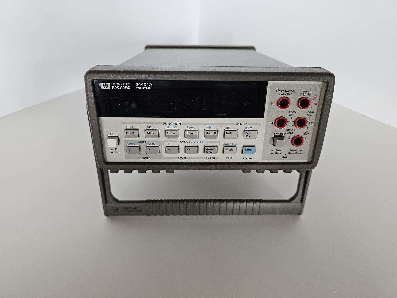
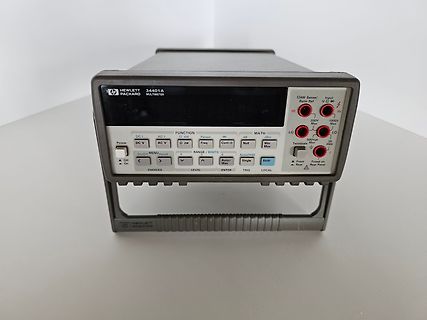
HEWLETT PACKARD 34401A MULTIMETER DC V AC V FUNCTION 2W Period Cont d MATH Min Max Ratio Ref Input V HI LO 200V 1000V Max 600Vpk Terminals 3A RMS Off On Off On Choices MENU Recall RANGE / DIGITS LEVEL ENTER Auto/Man Single Shift LOCAL TRIG
specified) Parameter Symbol Limit Values Unit Test Condition min. typ. max. Input-Interface Input REF Quiescent voltage V REFq – 200 – mV IREF = 0 μA Input resistance R – 6 – kΩ 0 V < V < 0.5 V REF REF Input FB Quiescent voltage V FBq – 200 – mV IFB = 0 μA Input resistance R – 6 – kΩ 0 V < V < 0.5 V
R3v2.0 Mirics Confidential 5 MSi001 3.3 RF Characteristics Unless otherwise stated the characteristics refer to the appropriate RF input pin and the signal at the I or Q output. Table 6: AM Port 1 Mode Tc = 25 ºC. VCC = VDD = 2RF= 1.8 MHz,IF = 450 kHBW= 200 kHz, unless otherwise stated Note Parameter Conditions
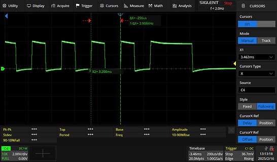
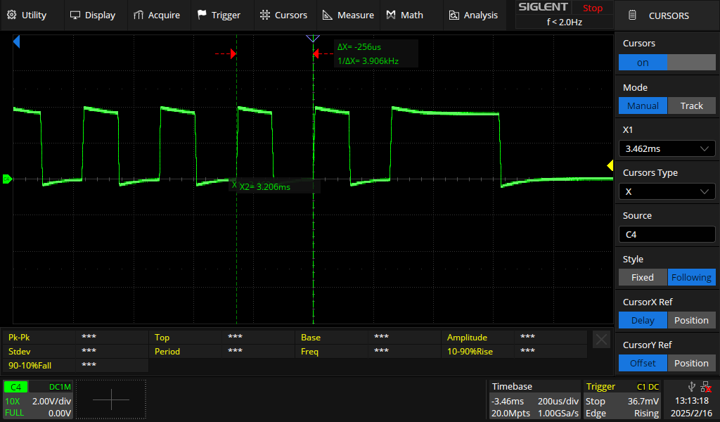
3.906kHz Cursors on Mode Manual Track X1 3.462ms Cursors Type X Source C4 Style Fixed Following CursorX Ref Position CursorY Ref Position Pk-Pk Stdev 90-10%Fall Top Period Base Freq Amplitude 10-90%Rise G4 10X FULL DC1M 2.00V/div 0.00V Timebase -3.46ms 200us/div Trigger Stop Edge Rising C1 DC 36.7mV 13:13
Features ϭ Miniature 12A 125VAC, 10A 250VAC/30VDC PCB Relay. ϭ UL/CUL, TUV, VDE approved. ϭ 450mW and 200mW coil are available. ϭ High CTI 250 material or product comply with IEC 60335-1 are available. ϭ Complies with RoHS-Directive 2011/65/EU. ϭ Optional for halogen free version. ϭ Optional for explosion-proof
n +85°C n ( T 300 T N 120 E E 600 +85°C E U 110 U 250 U C Y Y 500 L E E +25°C P 100 +25°C T T S B 200 B 400 90 +25°C -40°C -40°C 150 300 -40°C 80 70 100 200 3.0 3.5 4.0 4.5 5.0 5.5 1.5 2.5 3.5 4.5 5.5 1.5 2.5 3.5 4.5 5.5 SUPPLY VOLTAGE (V) BATTERY VOLTAGE (V) BATTERY VOLTAGE (V) SQW/CLKIN OUTPUT-VOLTAGE
-1 ÷ è REF ø (8) For this example, use Equation 9 and Equation 10. æ R ö VOUT = 1.23 ´ ç1 + 2÷ è R 1ø select • R1 = 1 k (9) æV OUT ö æ 24 V ö R 2 = R1 ´ ç -1 ÷= 1k ´ ç - 1÷ èV REF ø è1.23 V ø (10) R 2 1 k (19.51
= 25°C I = 2A 450 A A SW 500 ) 350 A400 V ( ( N350 400 G 300 E300 V T R (T O C250 S00 V 250 T C O E200 V T S 200 R 200 I150 T Q S 100 100 150 50 0 0 100 2.0 2.5 3.0 3.5 4.0 4.5 5.0 0 1 2 3 4 –50 –25 0 25 50 75 100 SWITCH CURRENT (A) SUPPLY VOLTAGE (V) TEMPERATURE (°C) 1302 G01 1302 G02 1302 G03 LT1302
= 25°C I = 2A 450 A A SW 500 ) 350 A400 V ( ( N350 400 G 300 E300 V T R (T O C250 S00 V 250 T C O E200 V T S 200 R 200 I150 T Q S 100 100 150 50 0 0 100 2.0 2.5 3.0 3.5 4.0 4.5 5.0 0 1 2 3 4 –50 –25 0 25 50 75 100 SWITCH CURRENT (A) SUPPLY VOLTAGE (V) TEMPERATURE (°C) 1302 G01 1302 G02 1302 G03 LT1302
The open-drain outputs directly drive the LEDs with maximum output sink current of 25 mA per bit and 200 mA per package (100 mA per octal). To blink LEDs at periods greater than 1.69 second the bus master (MCU, MPU, DSP, chip set, etc.) must send repeated commands to turn the LED on and off as is currently
Vorsicht bei billigen Multimetern geboten . Deren niedrige Strommessbereiche sind häufig mit einer 200 mA oder 250 mA Schmelzsicherung abgesichert. Schaltet man die Stromquelle versehentlich über 200 mA, beziehungsweise 250 mA, ist ein Sicherungswechsel fällig. Weblinks. Datenblatt von TI: LM317 3-Terminal
GND) eingestellt. Der Spannungsteiler wird dabei so dimensioniert, dass eine vorgegebene Spannung V ref (meist 1,25 V) gegen GND an der Anzapfung des Spannungsteilers abfällt, die dann zum Regeleingang des Linearreglers geführt wird. Dabei wird üblicherweise angenommen, dass der Strom I ref in den Regler

 Bild
Bild
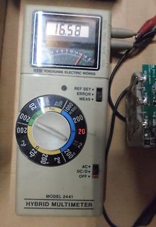
 Bild
Bild
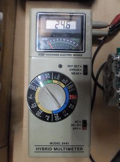
 Bild
Bild
 Bild
Bild
 Bild
Bild