mobility at zero substrate bias and adsV =dd cm /V −s 2 2 X2MS sens. of mobility to substrate bias ds V dd cm /V −s * X3MS sens. of mobility to drain bias at V =V cm /V −s * ds dd X3U1 sens. of velocity saturation effect on drain biasdst VddV µmV −2 * TOX gate oxide thickness µm TEMP temperature at which
R4 = 1kΩ T1 = IRF740, BUZ61 or load consisting of a 230-V, 8-W lamp can be R5 = 47kΩ BUK455-400B (V DS ≥ 400V) R6 = 1MΩ5 LED1 = LED, 5mm dia., red connected to high-voltage output, Without R7 = 100kΩ the lamp, the voltage onthe output shouldbe P1 = 500Ω preset, horizontal, lead Miscellaneous: approximately
DS3231 Extremely Accurate I C-Integrated 2 RTC/TCXO/Crystal General Description Benefits and Features 2 The DS3231 is a low-cost, extremely accurate I C ●● Highly Accurate RTC Completely Manages All real-time
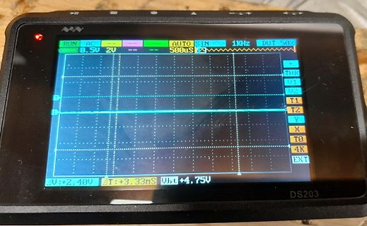
habe. Aber ein while (1) {GPIOF->ODR ^= GPIO_ODR_OD1;} bringt bei beiden nur rund 5MHz raus. (4,75 und 5,25) Beim 743 habe ich dann mal RCC_MCO_2 auf einen Port gelegt und auch bekomme ich nur diese Frequenz angezeigt. Interrupts sind aus und somit sollte der Port-Toggle doch eigentlich der
Aber ein > while (1) {GPIOF->ODR ^= GPIO_ODR_OD1;} > bringt bei beiden nur rund 5MHz raus. > (4,75 und 5,25) > > Beim 743 habe ich dann mal RCC_MCO_2 auf einen Port > gelegt und auch bekomme ich nur diese Frequenz angezeigt. > Interrupts sind aus und somit sollte der Port-Toggle > doch eigentlich
Pulse Width ≤ 1 µs C Duty Factor ≤ 0.1 % i r 30 D , Fig 10a. Switching Time Test Circuit I 20 V DS 10 90% 0 25 50 75 100 125 150 175 TC, Case Temperature ( C) ° 10% VGS d(on) tr td(off)f Fig 9. Maximum Drain Current Vs. Case Temperature Fig 10b. Switching Time Waveforms 10 )C h t ( 1 D = 0.50 e n
HKT05N10 HIGH VOLTAGE MOSFET (N-CHANNEL) FEATURES Low on-resistance:VDS100V,R DS(ON)115mΩ@V =10GSI =3A D Low Input Capacitance Fast Switching Speed Low Input/Output Leakage Surface Mount device MECHANICAL DATA SOT-23 Case: SOT-23 Case Material: Molded Plastic. UL flammability
) R 800 R C C500 T T P 600 P400 , , PS P – 400 –300 U U T T 200 O O E 200 R W W100 P P 0 0 0 25 50 75 100 125 150 175 0 25 50 75 100 125 150 175 200 S – CASE TEMPERATURE (°C) TS– CASE TEMPERATURE (°C) NOTE: These optocouplers are suitable for safe electrical isolation only within the safety limit data
) R 800 R C C500 T T P 600 P400 , , PS P – 400 –300 U U T T 200 O O E 200 R W W100 P P 0 0 0 25 50 75 100 125 150 175 0 25 50 75 100 125 150 175 200 S – CASE TEMPERATURE (°C) TS– CASE TEMPERATURE (°C) NOTE: These optocouplers are suitable for safe electrical isolation only within the safety limit data
habe ich auch schon gefunden: https://de.rs-online.com/web/p/schrittmotoren/8929167?cm_mmc=DE-PPC-DS3A-_-google-_-DSA_DE_DE_Automation_Index-_-Schrittmotoren%7C+Products-_-DYNAMIC+SEARCH+ADS&matchtype=&dsa-1697605355407&gclid=EAIaIQobChMI8MeQrsSngQMVy-93Ch2LuARNEAAYASAAEgKC7_D_BwE&gclsrc=aw.ds Nur
Außendurchmesser getriebeseitig: 14,0mm Außendurchmesser Außenseite: 13,7mm Innendruchmesser: 6,35mm Dicke: 4,75mm Weiß jetzt nicht ob man ohne genaue Bezeichnung da das passende Ersatzlage finden kann... Aber vielleicht reicht es auch die mit Öl zu behandeln?
0 V side V OUT = 0 V T j< 85 °C – – 50 µA V INH= 0 V V OUT = 0 V T j= 150 °C 4.2.3 Reverse diode V DS(HS) V IOUT = -9 A forward-voltage high – 0.9 1.5 T j= -40 °C side 1) – 0.8 1.1 T = 25 °C j – 0.6 0.8 T j= 150 °C Low Side Switch - Static Characteristics 4.2.4 On state low side R ON(LS) mΩ IOUT = -9
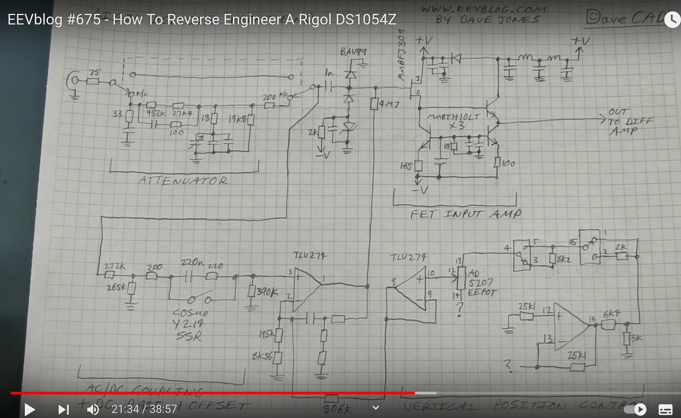
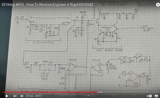
EEVblog #675 - How To Reverse Engineer A Rigol DS1054Z
WWW.EEVBLOG.COM BY DAVE JONES Dave CAL
75
33
953K
27K4
100
18
19K8
200
BAV99
In
+V
4M7
-V
ATTENUATOR
FET INPUT AMP
OUT TO DIFF AMP
165
100
277K
200
220K
220
TLV274
390K
13
4
15
5
8K2
2K
0
2
10
AD
current. The 2 2 output voltage drop when a load is added is determined by the parasitic resistance (R ds(on)of the MOSFET switches and the equivalent series resistance (ESR) of the capacitors) and the charge transfer loss between capacitors. S1 C1+ S2 VIN GND CIN C1 COUT GND S3 S4 C1- VOUT OSC. 2 MHz +
CFF ( 150 CIN OFF ADJ COUT u o GND R 2 GND o 100 r GND GND D 50 GND 0 Typical Application Circuit -75 -50 -25 0 25 50 75 100 125 150 Temperature (°C) Dropout Voltage vs Temperature for New Chip An IMPORTANT NOTICE at the end of this data sheet addresses availability, warranty, changes, use in safety-critical
current. The output voltage drop when a load is added is determined by the parasitic resistance (R ds(on)of the MOSFET switches and the ESR of the capacitors) and the charge transfer loss between capacitors. Details will be discussed in the following application information section. Figure 10. Voltage
Vielleicht kann man einen SN75LVDS86 verwenden, der die seriellen LVDS Signale in parallele Daten umwandelt, die man dann über GPIOs o.a. einlesen kann, um sie dann eventuell in der Auflösung angepasst in einem Framebuffer zur Darstellung abspeichern zu können. Fraglich ist, ob der SN75LVDS86 die niedrige Auflösung verarbeiten kann.
0A T A U 2.5 S 0.6 Y 18 I H F I I 0.4 17 RFEEDBACK= 10k M 2.4 W S 0.2 16 0 2.3 0 1 2 3 4 5 6 7 8 15–75 –50 –25 0 25 50 75 100 125 150 –75 –50 –25 0 25 50 75 100 125 150 TEMPERATURE (°C) SWITCH CURRENT (A) TEMPERATURE (°C) 1070/71 G04 1070/71 G05 1070/71 G06 Reference Voltage Feedback Bias Current Line
The goal of this example is to set the V DS monitor to trip at a current greater than 75 A. According to the CSD19535KCS 100 V N-Channel NexFET ™ Power MOSFET data sheet, the R DS(on)value is 2.2 times higher at 175°C, and the maximum R DS(on)
1000 o 1.4 1000 V ( e e 6 e e e c e e l u l l l n l l d o s n d s 1.2 V GS= 4.5 V, 4.6 A s n 2 - 4 V DS= 48 V 1 2 2 s 1 2 - R t 100 n 1.0 100 G O - 2 -) G ( 0.8 V D R 0 10 0.6 10 0 1.1 2.2 3.3 4.4 5.5 -50 -25 0 25 50 75 100 125 150 Q g Total Gate Charge (nC) T J Junction Temperature (°C) 2nd line 2nd line
A 0.041 0.052 a g V = 15 V, I = 5.3 A 24 S Forward Transconductance fs DS D Dynamic b Input Capacitance C iss 840 C V = 30 V, V = 0 V, f = 1 MHz Output Capacitance oss DS GS 71 pF Reverse Transfer Capacitance C rss 44 V DS = 30 V, GS = 10 V,DI = 5.3 A 17 25 Total Gate Charge
N-Channel 60-V (D-S), 175_C MOSFET FEATURES PRODUCT SUMMARY D TrenchFETr Power MOSFET V (V) r (W) I (A) DS DS(on) D D 175_C Maximum Junction Temperature D 100% R Tested 0.055 @ VGS = 10 V 4.5 g Pb-free 60 Available 0.075 @ VGS = 4.5 V 3.9 SO-8 D S D 1 1 8 1 G D 1 2 7 1 S D 2 3 6 2 G G D 2 4 5 2 Top View Ordering
Moin, Ich erhielt heute mit der Post ein paar DS3231 RTC Module. Bei der Inspektion fiel mir auf, daß anstatt der im Bild gezeigten "DS3231SN" die MEMS Versionen "DS3231M" verbaut sind: https://www.ebay.ca/itm/334976603309 Man kann sich also
, aber auch ohne VBAT-Pin. Und für den halben Preis vom DS3231 gibt's den RV-3032-C7 mit 2.5ppm, RAM, EEPROM und 0.75µA statt 3µA. S. L. schrieb im Beitrag #7483847: > Eigentlich ziehe ich den DS3231SN vor, und mit 4.60 EUR > für das Platinchen mit ihm
characteristics: V GS(th) Symbol Parameter Conditions Min Typ Max Unit VGS(th) gate-source threshold ID= 1 mA; V DS=V GS; Tj= 25 °C 2.4 3 3.6 V voltage ID= 1 mA; V DS=V GS; Tj= 175 °C 1 - - V ID= 1 mA; V DS=V GS; Tj= -55 °C - - 4.3 V The total spread, as per data sheet, is ∆V = 1.2 V or ∆V = ± 20 %. The SPICE model
Der Modus, bei dem nach jedem Byte NSS wieder auf 1 und zurück auf 0 gezogen wird können H74x & H75x auch, aber das nutzt für den ADS131M03 nichts. Bei einigen ST-Beispielen in CubeMX steuern die das NSS auch "manuell" = per Software an. Warum sollten sie das machen wenn es doch per Hardware funktionieren
Möglichkeiten vom DMA2D vernünftig ausnutzt => läuft Die RTC des H7 holt sich die Uhrzeit aus einem DS3231 => läuft, wird aber später durch Batteriepufferung der RTC des H7 ersetzt I2C-EEprom für sich öfter ändernde Status-Daten => läuft (kommt aber später evtl ins QSPI-Flash wenn mir was zum Wear-Leveling
TIA poa to MODENO. fr Cor ria NF E i(RoHS) 0 Gt0 D M 6 CFORMthSRSo:g uta Au cn ito yTe ew sl iu Di ds gn nt CUSmeMERDo APPROVAL _____________________________ _____________________________ 02101300-01-02 E M E R G I N G D I S P L A Y MODEL NO. VERSION PAGE TECHNOLOGIES CORPORATION E T 0 7 0 0 G 0 D M
n d th e fo ].lo w in g sc re e n a p p e a rs: J <TYPE>:#R4131A (50) R4131B (50) (A FC) R4131AN (75) R41318N (75) (AFC) <OPTION>: OBW off M o v e th e m ark "# " to th e R 4 1 3 1 A o r R 4 I3 IA N w ith th e E 3 keys. R4131B R41 31A R4131BN R4131AN rRIGGER P re s s th e key. J - A d ju s t th e v
Die 2A/T Sicherung war raus, und bei der Fehlersuche habe ich zwei defekte MosFets IRF840 gefunden (DS-Kurzschluss). Diese habe ich ersetzt, aber nach ca 10 Min im Betrieb war wieder Schluss. Schaltplan versuche ich gerade zu zeichnen..., poste ich wenn fertig. Die Schaltung basiert auf einem SG3525
hatte alle kritischen Kondensatoren getauscht: C1/C2 und C7/C8 Bauteile bei Mouse bestellt C1/C2 : R75PR4330AA30K C7/C8 : MKP1V014705BKSSD
Kann man die AREF beliebig klein wählen? Die zu messende Spannung wäre 0...75mV. Bedeutet bei 1,1V interne Referenzspannung ADC Werte bis 70. Die Genauigkeit ist nicht so wichtig (eher ne Abschätzung). Aber doch sehr klein. => würde man ARFE mit 0,3V wählen wären die ADC Werte
downloads/aemDocuments/documents/MCU08/ProductDocuments/DataSheets/ATmega48A-PA-88A-PA-168A-PA-328-P-DS-DS40002061B.pdf Arduino F. schrieb im Beitrag #7466282: > Auch finde ich keinen Hinweis auf den gültigen Aref Bereich. Seite 319, Tabelle 29-15 "ADC Characteristics" Von "dumm" war keine Rede
N&P-Channel Complementary Power MOSFET Product Summary ● VDS 30V ● RDDS(ON)at GS=10V) <95mohm ● R DS(ON)at GS=4.5V) <150mohm PMOS ● IDS -2.5A ● R DS(ON)at GS=-10V) <220mohm ● R DS(ON)at GS=-4.5V) ● 100% ▽V DSTested r General Description o ● High density cell design for lDS(ON) t ● High Speed switching
rein elektrisch funktionieren. Ganz ohne Elektrik. https://www.reichelt.de/entloetpumpe-soldapult-ds-017-deluxe-antistatisch-ds-017-ls-p225336.html?&nbc=1
0x00 BIT NAME FUNCTION 7:0 I2C_SLV4_DO[7:0] Data out when slave 4 is set to write. Document Number: DS-000189 Page 75 of 89 Revision: 1.3 ICM-20948 11.24I2C_SLV4_DI Name: I2C_SLV4_DI Address: 23 (17h) Type: USR3 Bank: 3 Serial IF: R Reset Value: 0x00 BIT NAME FUNCTION 7:0 I2C_SLV4_DI[7:0] Data read from
vorhin schon mal, wie Manuel auch vorschlägt, bei Synology nachgesehen. Der NASfinder schlägt das DS723+ vor, das kostet ohne Platten und mit 2GB Ram 500€ aufwärts. Aufgerüstet auf 16GB / 2x 4TB HDD wären das ~800€. Das haut natürlich schon rein. Dafür erspart die Oberfläche viel Frickelei...was den
Der H. schrieb im Beitrag #7464663: > HP Dynamic Smart Array B120i Ich bin mir zu 75% sicher, dass ich den selben in meinem Server hab. Die kann man überreden (ich hab dafür eine neuere Firmware flashen müssen... Ging mit den historischen Linux tools), dass die die Platten ohne raid
Y T 96.3 U U D 93.0 D 96.25 A A M 92.9 M 96.2 96.15 92.8 96.1 92.7 96.05 -40 -25 0 25 50 75 100 125 -50 -25 0 25 50 75 100 125 150 o TEMPERATURE ( C) o TEMPERATURE ( C) Figure 6. Max. Duty Cycle vs Temperature - "Y" Figure 5. Max. Duty Cycle vs Temperature - "X" 6 Submit Documentation Feedback

 Bild
Bild
 Bild
Bild
 Bild
Bild