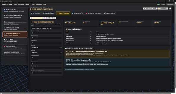
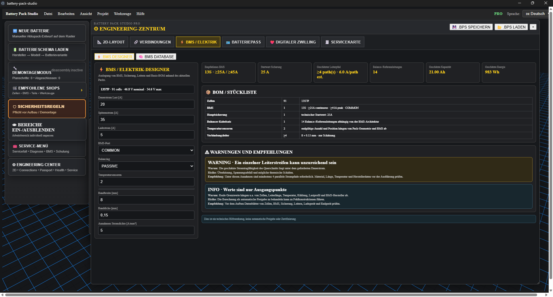
BATTERY PACK STUDIO PRO
ENGINEERING-ZENTRUM
BMS / ELEKTRIK
BMS DATABASE
BOM / STÜCKLISTE
135P
91 Zellen
46.4 V nominal
54.6 V max
20 A
25 A
4 path(s)
6.0 A/path
21.0 Ab
983 Wh
Watt (weniger wäre denke ich nicht tragisch, dann mixt die Mühle ebent etwas langsamer), Einbaumaße max. 10,5-11 cm Länge, 8x8 cm breit/hoch, ca. 3000 U/min, ein Teil aus einem Altgerät vllt., wenn der dann beim testen heiß wird oder es nicht bringt, wäre der fin. Schaden nicht besonders groß.
dass der Motor > ohne Belastung dreht, sind 150 Watt zu viel. Das wären dann geschätzt > 75% der max. Leistung. Und womit hast du die Leistung gemessen? Denn entscheident für die Beurteilung ist die Wirkleistung. Nicht dass du da die Scheinleistung gemessen hast...
lockout enter 6.5 7.0 7.5 V VDD_OVP VDD over voltage protection 26.0 27.0 28.5 V Max. Operating 25 V Voltage Current Sense Input Section TLEB LEB time 300 ns Vth_ocp_min Minimum over current threshold 485 500 515 mV Vth_ocp_max Maximum over current threshold 590 mV Vcs_min CS minimum threshold 135 mV FB Input Section Reference voltage for feedback Vref_FB threshold 2.475 2.500 2.525 V Tpause_min Minimum Toff 2.0 us F_min Minimum frequency 270 305 340 Hz F_max Maximum frequency 110 KHz Maximum
Symbol Min Typ Max Unit OFF CHARACTERISTICS Collector–Emitter Breakdown Voltage BC237 V 45 — — V (I = 2.0 mA, I = 0) BC238 (BR)CEO 25 — — C B BC239 25 — — Emitter–Base Breakdown Voltage BC237 V(BR)EBO 6.0 — — V (E = 100
Hysteresis V REGOVHYS 30 100 200 mV Oscillator Oscillating Frequency fOSC 450 500 550 kHz R RT00kΩ MAX DUTY1 D MAX1 82 90 98 % V MDT=L, VSYNC=0V MAX DUTY Cycle MAX DUTY2 D MAX2 42 50 58 % V MDT=H, VSYNC=0V MDT Pin Input High Level VIH_MD 0.8 x VREF - V REF+ 0.2 V MDT Pin Input Low Level V -0.3 - 0.2
tuning core as they does not implement core tuning. cod. SBK-50 useful space for the coil = 5,2 mm , max 10 turns , max wire Ø 0,3 mm, max inductance ~ 500 nH useful space for the coil = 5,7 mm , max 4,5 turns , cod. SBK-51 max wire Ø 0,6 mm, max inductance ~ 100 nH useful space price 0,45 € -- 0,40 €
character generator ROM (code 0101) T6963C−0101 is built in as standard. ▯External display memory : 64 KB Max The addresses in display memory of the text area, graphic area and external character generator area are determined by software. ▯Read or Write operations from the CPU do not disturb the display. ▯A
,See Figure 9 535 920 V(Rs)= 0 V, See Figure 9 100 135 Total loop delay, driver input to receiver (LOOP2) ou put, dominant to recessive RSwith 10 kΩ to ground, See Figure 9 155 185 ns R with 100 kΩ to ground,See Figure 9 830 990 S device control-pin characteristics
from exceeding the 135 - 180 (for 750 V GaN) 24 V rated maximum continuous drain voltage, a clamp circuit is needed 135 - 150 (for 900 V GaN) across the primary winding. The forward recovery of the clamp diode 21 www.power.com Rev. W 06/24 InnoSwitch3-EP 750 V = V MAX(NON-REPETITIVE) Safe Surge Voltage Typical margin (150 V) Region (SSVR) gives de-rating of >80% 650 V = V MAX(CONTINUOUS) V CLM VCLM< 90 V VOR 380 VDC V BUS Primary Switch Voltage Stress (264 VAC) PI
4bias, 1/8duty, frame frequency is 64Hz ⚫ Max.32×8 patterns, 8 commons, 32 segments ⚫ Built-in internal resistor type bias generator ⚫ 3-wire serial interface ⚫ 8 kinds of time base/WDT selection ⚫ Time base or WDT over flow output ⚫ Built-in LCD
LAND PATTERN (Unit: mm) L A A1 A2 θ 0.2 c Dimensions Dimensions Symbol In Millimeters In Inches MIN MAX MIN MAX A 1.050 1.250 0.041 0.049 A1 0.000 0.100 0.000 0.004 A2 1.050 1.150 0.041 0.045 b 0.300 0.500 0.012 0.020 c 0.100 0.200 0.004 0.008 D 2.820 3.020 0.111 0.119 E 1.500 1.700 0.059 0.067 E1 2.650
Kondensatoren muss wie folgt geachtet werden: Polyester: Vorheizphase: Tmax.125° C Lötphase: Tmax.135° C Polypropylen: Vorheizphase:max.100° C Lötphase: Tmax.110° C Wellenlöten Lotbadtemperatur: T P 260 ° C Einwirkdauer: t P 5 s Doppelwellenlöten Lotbadtemperatur: T P 260 ° C Einwirkdauer: t P 5
angle • 4.3~15.3 mm actuator • through hole SPECIFICATIONS parameter conditions/description min typ max units rated voltage 1 12 Vdc rated current 0.01 50 mA withstanding voltage for 1 minute 250 Vac contact resistance applying load of 2 times operating force at 5 Vdc, 10 mA 100 mΩ insulation resistance
Indicators PWR1, PWR2, PoE, FAULT, STATE, SIGNAL, WLAN, LAN Input/Output Interface Digital Inputs 2 Max. input current: 8 mA +13 to +30 V for state 1 +3 to -30 V for state 0 Alarm Contact Channels Relay output with current carrying capacity of 1 A @ 24 VDC Buttons Reset button Physical Characteristics Housing Metal IP Rating IP30 Dimensions 52.7 x 135 x 105 mm (2.08 x 5.32 x 4.13 in) 4 www.moxa.com Weight 860 g (1.9 lb) Installation DIN-rail mounting Wall mounting (with optional kit) Power Parameters Input Current 0.6 A @ 12 VDC, 0.15 A @ 48 VDC
@ 24 VDC Digital Input Channels 2 Digital Inputs +13 to +30 V for state 1 -30 to +3 V for state 0 Max. input current: 8 mA Ethernet Interface 10/100BaseT(X) Ports (RJ45 connector) EDS-508A Series: 8 EDS-508A-MM/SS Series: 6 All models support: Auto negotiation speed Full/Half duplex mode Auto MDI/MDI-X
256 MAC Table Size EDS-405A, EDS-405A-EIP/MM-SC/MM-ST/PN/SS-SC models: 2 K EDS-405A-PTP models: 8 K Max. No. of VLANs 64 Packet Buffer Size 1 Mbits Priority Queues 4 VLAN ID Range VID 1 to 4094 Serial Interface Console Port RS-232 (TxD, RxD, GND), 10-pin RJ45 (115200, n, 8, 1) DIP Switch Configuration
helix antenna 102 Chip antennas are especially small and can be built directly into a board (Figure 135 ). Generally, the RF characteristics of chip antennas are not as well suited for GNSS as patch or helix antennas. They target primarily low-cost and mass market applications. Figure 135: Chip antenna
Than MAX_FL Bytes and Bad CRC Statistic Register (ENET_RMON_R_JAB)....... 2053 57.5.71 Reserved Statistic Register (ENET_RMON_R_RESVD_0).......................................................................
R200 T 135 19 R616 T 37 21 D700 T 175 7 C305 B 132 56 C626 T 43 23 C826 T 40 53 C937 T 73 63 D701 T 156 32 L710 T 155 17 R201 T 129 46 R617 T 37 25 C306 B 119 55 C627 T 43 30 C827 T 37 70 C938 T 145 26 D702 T
IMR 14500 Zelle). Die LED Werte habe ich mit einem NT wie folgt ermittelt - 3,0V @ 70mA, 3,5V @ 135mA Bei 135mA wird die LED schon sehr warm (Fingertest) und da an der Rückseite keine Kühlfläche angebracht ist, wollte ich mit mehr Spannung/Strom keine Zerstörung der LED riskieren. Auf der
vorhanden sind, wäre schon diese den Preis > wert. Naja, da gilt es das Datenblatt zu beachten, also max. 0,2C, beim Laden ab cv max 40 mA, Endladen auch max 0,2C (120 mA) und Ende bei 3 V. Frage ist, ob die verbaute Elektronik das insb. bzgl. der Abschaltung einhält, könnte man aber in Serie testen
gelten und nicht für 1/10 davon, denn der Leckstrom steigt genau um den mehrfachen wert an, aber der max. Rippelstrom dafür nur um das Doppelte. Falsche Parametrierung der Bauteile führen dann schon zum vorzeitigen Ausfall, ich habe davon genug solcher Fälle, wie oben geschildert, erlebt. Wenn man zig
raten: https://www.mouser.de/ProductDetail/Nichicon/UBW1H471MHD?qs=Wu4QelNNmeMKJYngndrUWw%3D%3D 135C und kann mehr Ripple ab, 1650mA bei 135C https://www.mouser.de/datasheet/3/497/1/e_ubw.pdf
gleich vom Start weg halbwegs richtig geht. Normalerweise geht der ntpd davon aus, dass die Uhr um max. 128 ms falsch geht, sonst ist die wohl defekt.
DCF ???: t.b.d. diverse Pull-Down: 1.2 mA ALS SFH5711: ca. 0.5 mA RS-232 MAX3223E: < 1.3 mA ohne Last RS-485 MAX3079E: < 1.5 mA unterminiert 4x LDO MIC5236: < 0.12 mA 3x Referenz REF3433: < 0.3 mA OP INA186A1Q: ca. 0.2 mA was-ich-noch-vergaß: ?[/pre]
5V ± 10%; VPPP = VCC ) M2tCe001 Symbol Alt Parameter Test -55 (2) l-70 -80 -90 Unit Condition o Min Max s Min Max Min Max Min Max t t 55 70 80 90 ns AVQV ACC to Outputalid G = VIL - O Valid IL ) ( s ELQV tCE Chip Enable c = VIL 55 70 80 90 ns Valido Outputu o d GLQV tOE OutputEnable E = VIL 30 35 40 40
215˚C 0 8 4 A Electrical Characteristics D The following specifications apply fCC 5 VDC , MIN≤TA≤T MAX and fCLK=640 kHz unless otherwise specified. C 0 Parameter Conditions Min Typ Max Units 0 ADC0801: Total Adjusted Error (Note 8) With Full-Scale Adj. ± 14 LSB 5 (See Section 2.5.2) 1 ADC0802: Total
taken with nominal devices at room temp). 1V8_IN 3V3_IN PARAMETER TEST CONDITIONS UNIT TYP MAX TYP MAX 1 DSSS TX Power = 17.9dBm 92 270 310 6 OFDM TX Power = 17.8dBm 110 170 270 320 54 OFDM TX Power = 15.5dBm 115 215 Continuous TX(1) HT MCS0 TX Power = 17.8dBm 110 270 mA HT MCS7 TX Power = 15.5dBm
routine examines the Rdown and Rup bits in the range control status register. Ifthe range > range max. then the instrument must range up. Ifthe range < range min. then the instrument must range down. Italso ensures that in the TRIGGER LEVEL function only manual ranging isallowed. 1.4.1.4. M e a s u
button “zero set on/off” 1.6. D C C U R R E N T M E A S U R E M E N T S Ranges :20mA,20mA,2.4,208 (max, input current in highest range) #10 A (20 A for max, 20 sec.) Resolution 510HAin20mArange Number of representation units £2200 Acuracy ++(0.5%ofreading+0.1%offulscale) Temperature coefficient +0.05%
mitm INA849 einen Vorverstärker gebaut, ein Anti-aliasing-Filter mit einem LTC1678 und mit einem DRV135 ein symmetrisches Signal erzeugt. Ein Hochohmiger AKG-Kopfhörer lies vermuten, dass irgendetwas nicht stimmt, weil man nichts gehört hat. Aber ja - es hat halt nur nicht wahrnehmbar gerauscht. Wenn
24 Bit auf der digitalisierten Audioseite, ermöglichen können. Die 192 kHz ist die Abtastrate f_{max} = f_s/s; dies gilt nach Nyquist-Shannon-Abtasttheorem. Also, f_s = 192 Khz: f_{max} = 192 KHz /2 = 96 kHz = 96.000 Hz. Das sehen wir im Bild (05_Schlaffzimmer_01.05.2026.jpg).
deutlich steigen, allerdings auf Kosten der Empfindlichkeit. Geläufige Typen. Bezeichnung Gehäuse Vce (max) [V] Vsupply [V] CTR [%] Iout [mA] Geschwindigkeit Bemerkung Lieferant Datenblatt 4N25 4N26 4N27 4N28 DIP6 30 — 20, 10 ton/off 2 µs (typ.) B C D DK e F U R Broadcom CT-Micro Everlight Isocom LiteOn
µs B C D DK e F U R Broadcom CT-Micro Everlight Isocom LiteOn ONSemi QT-Brightek Toshiba Vishay 6N135 6N136 PS8501 DIP8 20 15 30 100 1 MBit/s Dual-channel: HCPL-xx3x B C D DK F P U R Broadcom Cosmo CT-Micro Everlight Isocom LiteOn ONSemi Renesas Toshiba Vishay HCPL-0500/1 EL0500/1 ICPL0500/1 SFH6315
measure anode luminous sensitivity) VOLTAGE 0 V ON LIGHT LEVEL OFF 5 6 7 8 9 (minutes) 1 µA ANODE I max. OUTPUT Ii I min. OR Ii I max. I min. 5 6 7 8 9 (minutes) WARM-UP PERIOD (5 minutes or more) THBV4_0440EA Figure 4-40: Light hysteresis In light hysteresis test, the photomultiplier tube is operated
packaging E1 D 2 n 1 α E A A2 L c A1 β B1 p eB B Units INCHES* MILLIMETERS Dimension Limits MIN NOM MAX MIN NOM MAX Number of Pins n 8 8 Pitch p .100 2.54 Top to Seating Plane A .140 .155 .170 3.56 3.94 4.32 Molded Package Thickness A2 .115 .130 .145 2.92 3.30 3.68 Base to Seating Plane A1 .015 0.38 Shoulder
regulates its output (V OUT –) to –0.94 • V IN_N . In Burst Mode operation the LTC3265 draws only 135µA of quiescent current with both LDOs APPLICATIONS on. In constant frequency mode, the boost and inverting charge pumps produce outputs equal to 2 • V and nn Low Noise Bipolar/Inverting Supplies IN_P
3 6.49K VREF+ V- 15 VREF- R134 C76 GND 6.49k u +5V 0.01uF 7 . C 0 GND 7 K Q56 PHASE-MATCH U-LOAD1 R135 1 6 2N2907 49.9K 2N2222 R 4 Q54 3 K C91 R 1 GND 0.1uF 2N2222 Q55 GND GND Abbildung 20: Schaltung zur Erzeugung der Sinus-Referenz und zur Überwachung der Phasenlage Der originale Mikrocontroller besitzt
Märchen, von seiner SpaceX Chefin Cwen Shotwell 2018 vollmundig angekündigt. Sollte bis spätestens 2028 (max. 10 Jahre) laufen. Naja. https://youtu.be/ENBn-W3uPXQ?si=TVhut3L5n0Rinz9r Den Rest schenke ich mir mal. Nur mal so als Abschluß. SpaceX nannte für all seine Unternehmen einen totalen addressierbaren
Jahre alter SciFi über ferngesteuerte Boxroboter: https://www.youtube.com/watch?v=6LyGYPbTcVA&t=135s und er Weg ins "Real": https://www.youtube.com/watch?v=P8U_4v8SUOQ
be1 to 4.Default value is 4. Byte8: Maximum Power ThisvalueisreportedintheConfigurationDescriptor:bMax-Powerfieldandisthecurrentin2mAincrements thatisrequired from the upstream hubs.Theallowedrangeis 00h (0 mA)to FAh(500mA).Default value is 32h (100 mA) Byte9–15: Reserved Set to FFh (except 11 which
0,46) .075 .219 .015 0 Dia. Ref. (Ref.) (5,56 0,38) 8 .400 .300 .010 : (10,16) Figure 1 (7,62 0,25) e Max. r l Solder Pocket c .410 .038 .150 o (10,41) (I.D.) x (Deep) L Max. i t u .025 O (1,32 0,08) Sq. Typ. 0 Solderless Wrap 9 8 .135 8 Max.3) .510 .015 ) (12,95 0,38) 5 .600 ( (1Max.) : Figure 2 c f O
Nach Abschrauben des Kühlkörpers ist die Rückseite der Platine zugäng- • Gleichspannungsmessgerät U max≥ 50 V lich. • Gleichstrommessgerät I max≥ 500 mA Unter dem Messinstrument befindet sich der Um- schalter S3, mit dem das Instrument als Span- 3.3.2 Abgleich 30 V Ausgangsspan- nungsbereich nungs- oder

 Bild
Bild