(0 « « f M« -»«m1iIkM I ----------». v T . ZPS P . t < M g riff» t V T -Pro ^ 'G » *m x lg RAM p ,ß o r-C « '*»" " I*“ ««•ticrtfiit i Z P S - O c f — - j . Bild 2. Prinzip des digitalen Kennungssystems „ZPS" Bild 4. Prinzip eines Speicherfernsehers ------- 'Tor MQNiTCP ] aAfl JE L « IByle . 8 Bit (
Group 63 1994-05-01 SAB 80C517A/83C517A-5 A/D Converter Characteristics V CC = 5 V + 10 %, – 15 %; V SS = 0 V VAREF = V CC 5%; VAGND = oSS 0.2 V; T A= 0 to 70 C for the SAB 80C517A/83C517A-5 T A= – 40 to 85 oC for the SAB 80C517A-T3/83C517A-5-T3 T =– 40 to 110 C for the SAB 80C517A-T4/83C517A-5-T4 A Parameter
No Need WAMPU6 V5.11 CYPRESS MPU/MCU CY7C66013(SSOP48) ADP-CY7C66XX-SS No Need WAMPU6 V5.11 CYPRESS MPU/MCU CY7C66111 ADP-CY7C66XX-SS No Need WAMPU6 V5.11 CYPRESS MPU/MCU CY7C66112 ADP-CY7C66XX-SS No Need WAMPU6 V5.11 CYPRESS MPU/MCU CY7C66113 ADP-CY7C66XX-SS No Need WAMPU6
VB3-W, VD4 = V DD -V SS , terminal voltage. *3 Flatness of the heat-sink should be lower than 0.15mm. *4 The test condition is AC 2500V, 1 second. Electrical Characteristics at Tc=25°C, VD=15V Parameter Symbol Conditions min
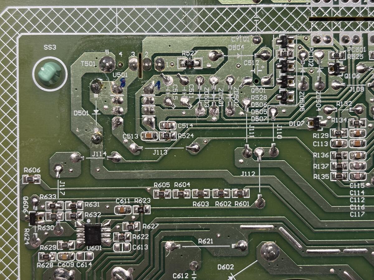
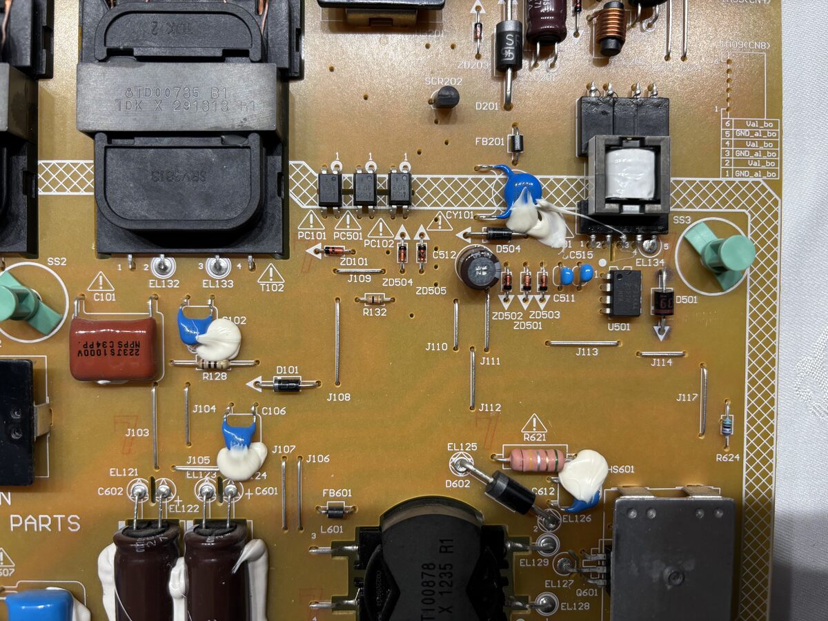
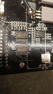
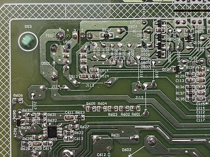
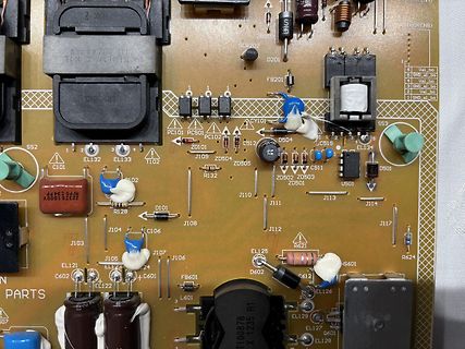
mir vor einer knappen Woche einen Panasonic TX-P65VT50E auf Kleinanzeigen für 15€ gekauft mit einem SS-Board Fehler (8x blinkte die Power LED). Allerdings reichte es aus, die Kabel am SS-Board einmal ab und wieder dran zu machen. Ein SS-Board kaufte ich mir allerdings schon davor. Als es dann gestern
ich es heute einbaute funktionierte der TV bei einem schnellen Test auch problemlos mit dem neuen SS-Board. Da er funktionierte habe ich die restlichen Schrauben fest gemacht und ihn wieder hingestellt. Und auf einmal bekam ich kein Lebenszeichen mehr von ihm. Ich habe dann das alte SS-Board wieder
K1×Vcc (K1=0.45) Then we can have: V05 www.microne.com.cn Page 10 of 19 ME4056 For example, NCP03YS110 , operating Temperature is -40℃ to 125℃. If using environment temperature is -25℃ to 125℃, then R TLis the value of the resistance of NCP03YS110 at -25℃, about 66.148Ω; R =is thTHvalue of the resistance of NCP03YS110 at 125℃, about 1.077Ω. Likewise, for positive temperature coefficient thermistor in battery, we haveTH >R TLand we can calculate: We can conclude that temperature monitor range is independent of power
mA V COMP=1.25V, VFB1.5V Output Source Current ICMPSO 100 180 - μA V COMP=1.25V, VFB0V Soft Start SS Pin Source Current SSSO 1.4 2 2.6 μA V SS.5V SS Pin Sink Current I 5 12 - mA V =0.5V SSSI SS Power Good Signal Output PGDB Pin Output Low Level Voltage VPGBOL - - 0.4 V PGDB=1mA PGDB Pin Leak Current
Check signal Input Test input. Usually open T1 , T2 VDD ― Power supply (5.0 V) V ― Power supply (0 V) SS 4 2002-01-07 T6963C Functional Definition ● After power on, it is necessary to reset. RESET is kept L between 5 clocks up (oscillation clock). ● When HALT ▯ L, the oscillation stops. The power supply
Familie Wiesbaden schen Akustik Meistertitedie Berechtigung sind inden dreiFarben gelb, Brunhildenstr.110 Dr.-Ing.IVeit zum Führen der Berufsbe rotund grün lieferbar. 6200 Wiesbaden 19.03.-21. 03. 86 zeichnung „Geprüfter Blitzab Die vierstelligeModule sind Tel.:06121/702661-62 Radar - heute leitersetz
. . . . . . . . . . . . . . . . . . 5 V 5% or DV (AV , DV ) . . . . . . . . . . . –0.3 V to +6.0 V SS DD DD All inputs within the range: .AV SS – 0.5 V Vin Stresses above those listed under Absolute Maximum Rat AV DD + 0.5 V, or ings may cause permanent device failure. Functionality at or DV SS – 0.5
occurs. SOA Protection P: Primary Chip In the event that there are two consecutive cycles where the 110% S: Secondary Chip I is reached within ~500 ns (the blanking time + current limit delay Start LIM P: Powered Up, Switching time) (including leading edge current spike), the controller will skip 2.5
95: _ 96: ` 97: a 98: b 99: c 100: d 101: e 102: f 103: g 104: h 105: i 106: j 107: k 108: l 109: m 110: n 111: o 112: p 113: q 114: r 115: s 116: t 117: u 118: v 119: w 120: x 121: y 122: z 123: { 124: | 125: } 126: ~ 127: 128: Ç 129: ü 130: é 131: â 132: ä 133: à 134: å 135: ç 136: ê 137: ë 138: è 139
r T n t « n S w i e w g m S w i c K a n A R »< a – G e n „ s A e e I l s M – E » »V » b Z u K D » ß D a – w G r u D a – N » – a M e n e e a e l i e A e d S 6 B a Ws d g a w B C g A 1 2 3 4 5 6 7 e ) . r d d . d . - n l . « a e d u u « d u e n u « e n C l . l e . e « K i « t « e n »< u e r « t « ß n
900ss schrieb im Beitrag #8050419: > Ich hätte 2mm Lot im Dachdeckerforum angeboten ;) Dürfen die noch bleihaltig löten? Würde aber wohl letztendlich nicht auffallen bzw. keinen interessieren.
900ss schrieb im Beitrag #8050419: > Ich hätte 2mm Lot im Dachdeckerforum angeboten Die haben die Legierung andersherum Pb60-Sn40 und benutzen Stangenware ohne Flußmittelkern.
Demmig Fourierreihen Demmig Verlag 1983 92 S. G. Demmig Matrizen und Determinanten Demmig Verlag 1994 110 S. G. Demmig Komplexe Zahlen I Demmig Verlag 5. Aufl. 1995 77 S. G. Demmig Komplexe Zahlen II Demmig Verlag 2. Aufl. 1982 90 S. G. Demmig Vektorrechnung I Demmig Verlag 1985 102 S. G. Demmig Vektorrechnung
incorporate minor changes in detail from the i n f o r m a t c o n t a i n ind this m a n u a l . T H I SS E R V I CM A N U AR E P L A C E S : - the first edition Service Manual 4822 872 35302 - the s e c o n e d i t i oS e r v i M a n u a 4 8 2 2872 3 5 3 1 2 - Service note SME 126, 4822 872 38308 - Service
>110V isdisplayedasOLand 0.08 reference 1 m W in reference resistor or when selecting the relative reference function with push button ‘zero set on/off” Reference resistors £80, 75, 93, 110, 125, 136, 150
this pin and V SS Disable Keep float Connect to external Connect to external V CC charge pump V DD source source BGGND P Reserved pin. It should be connected to V SS C1P/C1N I C1P/C1N – Pin for charge pump capacitor;
this pin and V SS Disable Keep float Connect to external Connect to external V CC charge pump V DD source source BGGND P Reserved pin. It should be connected to V SS C1P/C1N I C1P/C1N – Pin for charge pump capacitor;
is in good working order. Display on FLA remote control and monitor P200 f (Hz) v (km/h) settings U ss (V) f (Hz) Required min max Required min max 4 200 200 195 205 7.2 7.0 7.4 8 400 400 393 407 14.4 14.1 14.7 16 1600 1600 1581 1619 57.6 56.9 58.3 32 6400 6400 6333 6467 230.4 227.9 232.8 Adapter cable
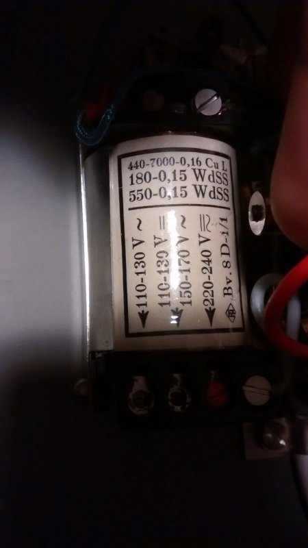
gibt. Das Thema ist nur noch die Verschaltung, insbesondere wenn man mit einer Batterie -- die NICHT 110..130V DC hat -- nutzen will.
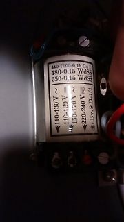
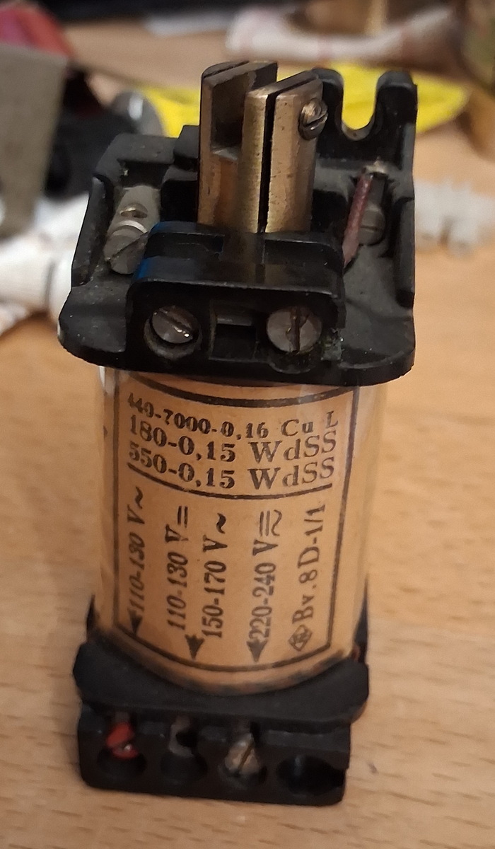
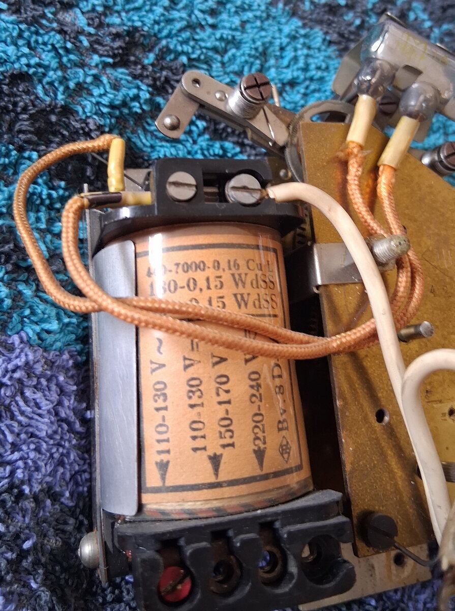
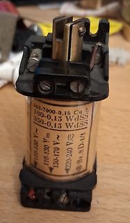
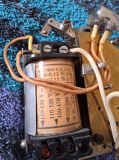
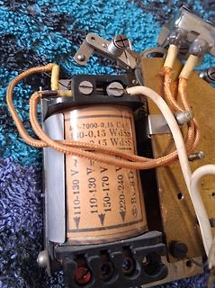
Kupferlackdraht Die anderen zwei Wicklungen sind einfach nur zwei Widerstände, 180 - 0,15 WdSS 180 Ohm 0,15mm Widerstandsdraht 550 - 0,15 WdSS 550 Ohm 0,15mm Widerstandsdraht Die Widerstandsdrähte sind bifilar gewickelt, damit sie kein Magnetfeld erzeugen. So etwas findet man öfters
auch, ab welcher Lademenge der Ladestrom sinkt. Bemerkung 1: um 74Wh voll zu Laden, werden bestimmt 110% benötigt. Bemerkung 2: eine 74Wh Powerbank hat nach ein paar Ladezyklen oft viele % weniger Kapazität. An einer Charmast Powerbank 23,8Ah 88,1Wh, die einen Laptop mit 20V 3,25A laden kann, habe
worden. GaN ist auch drin: https://www.reddit.com/r/ChargingSheet/comments/1pxqgyk/ikea_sj%C3%B6ss_20w_charger_review_and_teardown/ Das fängt an mit 4 Euro für ein 20-Watt-PD-Netzteil (liefert bis zu 15 V) und geht über ein 65-Watt-Netzteil für 13 Euro (liefert bis zu 20 V und kann im Bereich von
------------- Connection Index : 0x03 (3) Length : 0x10 (16 bytes) SupportedUsbProtocols : 0x03 Usb110 : 1 (yes, port supports USB 1.1) Usb200 : 1 (yes, port supports USB 2.0) Usb300 : 0 (no, port not supports USB 3.0) ReservedMBZ : 0x00 Flags : 0x00 DevIsOpAtSsOrHigher : 0 (Device is not operating at SuperSpeed or higher) DevIsSsCapOrHigher : 0 (Device is not SuperSpeed capable or higher) DevIsOpAtSsPlusOrHigher : 0 (Device is not operating at SuperSpeedPlus or higher) DevIsSsPlusCapOrHigher : 0 (Device is not SuperSpeedPlus
------------- Connection Index : 0x03 (3) Length : 0x10 (16 bytes) SupportedUsbProtocols : 0x03 Usb110 : 1 (yes, port supports USB 1.1) Usb200 : 1 (yes, port supports USB 2.0) Usb300 : 0 (no, port not supports USB 3.0) ReservedMBZ : 0x00 Flags : 0x00 DevIsOpAtSsOrHigher : 0 (Device is not operating at SuperSpeed or higher) DevIsSsCapOrHigher : 0 (Device is not SuperSpeed capable or higher) DevIsOpAtSsPlusOrHigher : 0 (Device is not operating at SuperSpeedPlus or higher) DevIsSsPlusCapOrHigher : 0 (Device is not SuperSpeedPlus
anderen Code ansehen ... https://github.com/libdriver/ssd1315/blob/main/src/driver_ssd1315.c#L110 Da taucht das Bit D/C# auf, wenn auch nicht als #define, sondern als Konstante 0x40.
das Leerzeichen. > > 95 * 8 = 760 Byte eben und wenn man genau schaut bleiben nur 69 über mit ß und Ziffern Space muß man nicht kodieren, na gut wer es mag -> 70 und nicht als 8 x 8 Matrix sondern als 7 x 5 und kann das Leerpixel auch on the fly hinzufügen. ergo komme ich auf viel weniger Byte
Konstanz des Ausgangsstro- ≤0,05 % bei Netzänderung von ±10 % mes ≤0,5 mA bei Laständerung um 100 % ≤2 mV ss bei Konstantspannungsbetrieb Restwelligkeit ≤0,1 mA ss bei Konstantstrombetrieb Ausregelzeit ≤20 ms bei Laständerung um 100 % Netzversorgung Netzspannung 220 V, 50 Hz Eingangsspannungsbereich 198 … 242
VCC to SS (cathode connected to VCC , anode to SS). Schottky diode 1N5817 is recommended for through hole and MBRS120T3 is recommended for surface mount. Figure 10. Supply voltage protection VCC V CC 0.1µF DEVICE
900ss schrieb im Beitrag #8028218: > . > Das ganze hat so ca. 3-4 Stunden gedauert. Naja, 4h für 300 Zeilen für die es wahrscheinlich Massen an Beispielen im Netz gibt... 900ss schrieb im Beitrag #8028237
offenbar viel besser klar, und erst zum Schluss übersetzen könnte bessere Ergebnisse liefern. 900ss schrieb im Beitrag #8028237: > -fpack-struct Hat das überhaupt ne Auswirkung beim AVR? 900ss schrieb im Beitrag #8028237: > -Wno-array-bounds Gefährlich 🤔 Die heiße Frage ist jetzt was
VDD(PVDD) VDDA = VDDD = VDD(TVDD); 2.5 3.3 3.6 V V digital supply voltage VSSA = VSSD = VSS(PVSS) V SS(TVSS) 0 V 2.5 3.3 3.6 V DDD V DD(TVDD) TVDD supply voltage 2.5 3.3 3.6 V [3] V DD(PVDD) PVDD supply voltage 1.6 1.8 3.6 V V DD(SVDD) SVDD supply voltage VSSA = VSSD = VSS(PVSS) V SS(TVSS) 0 V 1.6 - 3.6
VorMontagebeginnIstdas ToraufFunktion sowie Leichtgängigkeitzuprüfen und einzustellen.Das Tor m u ß im Handbetriebgleichmäßig und ruckfreilaufen.Zur Resultatsverbesserungsind dieTorgelenkeundbewegli chen Stellenzu ölen. Beim BefestigendesToran 14.1 schlußbleches(8)diezutref fendeEinbausituation(13.1
voltage below - 1.25 V. 2N5640 1.0 k Control V V R 1 ref R2 ref Omax + DSS DDS Minimum V out 1.25 V V SS V O BV DSS+ 1.25 V + SS, ILmin- DSS < O < 1.5 A. * 1 protects the device during an input short circuit. As shown 0 < O < 1.0 A. Figure 21. Adjustable Current Limiter Figure 22. 5.0 V Electronic Shutdown

 Bild
Bild
 Bild
Bild
 Bild
Bild
 Bild
Bild
 Bild
Bild
 Bild
Bild
 Bild
Bild