-
 Bild
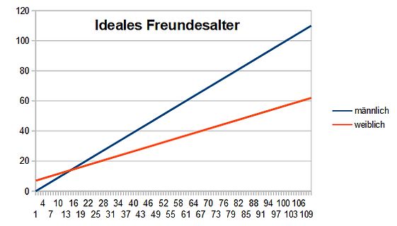
Liniendiagramm zum idealen Freundesalter nach Geschlecht
Ideales Freundesalter männlich weiblich 0 20 40 60 80 100 120 4 1 10 7 16 13 22 19 28 25 34 31 40 37 46 43 52 49 58 55 64 61 70 67 76 73 82 79 88 85 94 91 100 97 106 103 109
in „Mathematik 4.Klasse“ · Offtopic · · Diagramme
-
 Bild
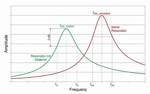
Diagramm der Resonanzfrequenz eines Resonators mit und ohne Material
Amplitude fres_unloaded leerer Resonator fres_loaded 3 dB Resonator mit Material flu fuu fuo Frequenz
in „Streufeldresonator: seltsames Messergebnis“ · HF, Funk und Felder · · Diagramme
-
 Bild
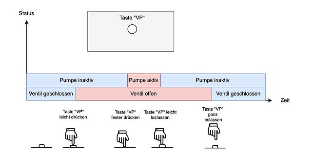
Diagramm zum Tastendruck und Systemstatus
Status Zeit Taste "VP" Pumpe inaktiv Pumpe aktiv Pumpe inaktiv Ventil geschlossen Ventil offen Ventil geschlossen Taste "VP" leicht drücken Taste "VP" fester drücken Taste "VP" leicht loslassen Taste "VP" ganz loslassen
in „Drucktaster mit mehreren Ebenen (?)“ · Analoge Elektronik und Schaltungstechnik · · Diagramme
-
PDF
-
 Bild
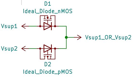
Schaltplan einer idealen Dioden-OR-Verknüpfung mit MOSFETs
D1 Ideal_Diode_nMOS Vsup1 D2 Ideal_Diode_pMOS Vsup2 Vsup1_OR_Vsup2
in „Ideale Diode Symbolvorschlag“ · Platinen · · Schaltpläne
-
 Bild
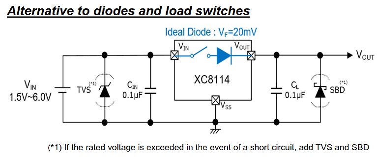
Schaltplan einer idealen Diode mit XC8114
Alternative to diodes and load switches Ideal Diode : VF=20mV VIN 1.5V~6.0V TVS CIN 0.1uF XC8114 VIN VOUT VSS CL 0.1uF SBD (*1) If the rated voltage is exceeded in the event of a short circuit, add TVS and SBD
in „Neue Bauteile: DB9-Stecker mit Push-Pull, m5Stack-Module, Kelvinklemmen uvam“ · Mikrocontroller und Digitale Elektronik · · Schaltpläne
-
 Bild
Werbebanner für MEMS-Plattform von ideal switch
ideal switch MEMS platform for power applications Seamless adaptation from milliwatts to megawatts. High power handling Low power consumption Tiny, fast and silent High reliability
in „Drohnen-Innovation, Raspberry Pi OS-Update und Python in Hardware“ · Mikrocontroller und Digitale Elektronik · · Sonstiges

-
 Bild
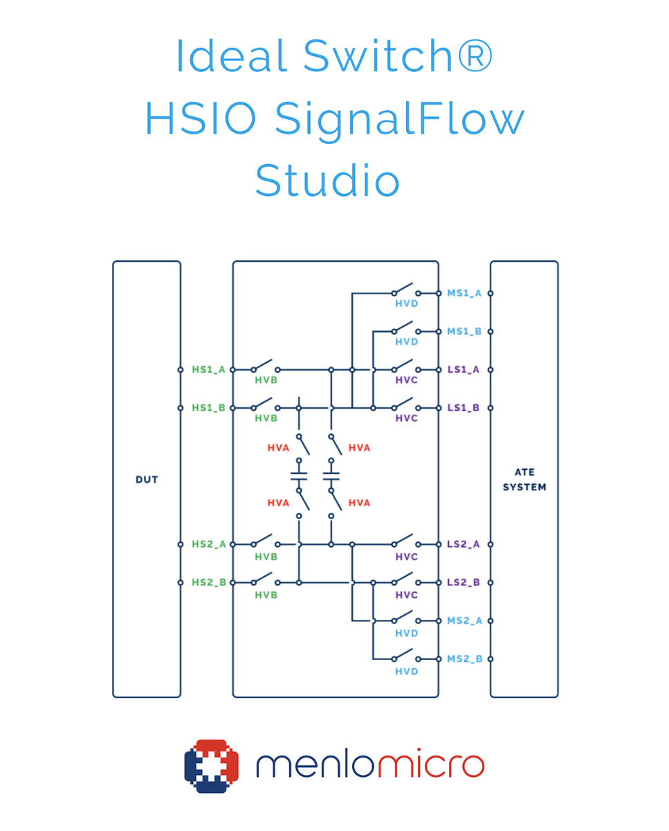
Schaltplan eines Ideal Switch HSIO SignalFlow Studio
Ideal Switch® HSIO SignalFlow Studio DUT HS1_A HS1_B HS2_A HS2_B HVA HVB HVC HVD LS1_A LS1_B LS2_A LS2_B MS1_A MS1_B MS2_A MS2_B ATE SYSTEM menlomicro
in „AMD-AI-Keynote, Amper heruntergeskillt, PCIe 7.0 und AI-Ethernet“ · Mikrocontroller und Digitale Elektronik · · Schaltpläne

-
PDF
filter.pdf
skrf as rf %matplotlib inline from pylab import * rf.stylely() from skrf.calibration import SOLT my_ideals = [ rf.Network('filter/ideals/load_ideal.s2p'), rf.Network('filter/ideals/open_ideal.s2p'), rf.Network('filter/ideals/short_ideal.s2p'), rf.Network('filter/ideals/thru_ideal.s2p'), ] my_measured =
-
PDF
filter-design-report-65.pdf
A1_S2 Texas Instruments Inc. OPA4187 GbwTyp= 0.55MHz 1 VccMax= 36V VccMin= 4.5V 3. C1_S1 Generic Ideal Cap= 100.0 nF 1 Tolerance= 2.0 % 4. C1_S2 Generic Ideal Cap= 215.0 nF 1 Tolerance= 2.0 % 5. C2_S2 Generic Ideal Cap= 187.0 nF 1 Tolerance= 2.0 % 6. R1_S1 Generic Ideal Res= 13300.0ohm 1 Tolerance=
in „Suche "Filtertabelle"“ · Analoge Elektronik und Schaltungstechnik ·
-
PDF
LTspice-Trafos.pdf
wurde im Internet entdeckt und entsprechend umfunktioniert). 56 8.2.2. Einpuls-Gleichrichter mit idealem Trafo Aufgabe: Untersuchen Sie ein Netzteil mit idealem Netztransformator, Gleichrichterdiode, Lastwiderstand RL = 1kΩ und Ladekondensator C = 100µF. Der Trafo-Eingang liegt an der Netzspannung mit
in „IKEA Kurbellampe defekt?“ · Analoge Elektronik und Schaltungstechnik ·
-
PDF
VortragStabantenne_DF4EU.pdf
ground plane = GP bzw. Stabantenne). Bild 3: Elektrische Feldlinien um die ▯/4 –Stabantenne 2. Die ideale ▯/4 –Stabantenne Bild 4: Die ideale ▯/4 –Stabantenne Wie der Name sagt, ist diese Antenne genau eine Viertelwellenlänge lang (h= ▯/4). Der Stabdurchmesser d ist sehr viel kleiner als die Stabhöhe h
in „Groundplane-Antenne auf Dachlüfterhaube“ · HF, Funk und Felder ·
-
 Bild
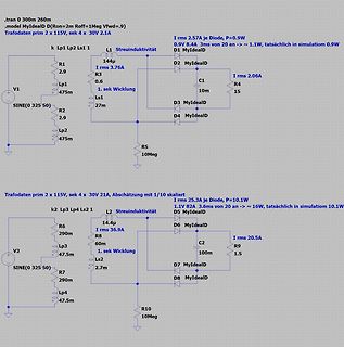
Schaltplan zweier Transformator-Gleichrichter-Stufen mit Simulationswerten
R3 0.6 1. sek Wicklung Ls1 27m D1 MyIdealD D2 MyIdealD C1 10m R4 15 D3 MyIdealD D4 MyIdealD V1 SINE(0 325 50) R2 2.9 Lp2 475m Lp1 475m R5 10Meg Trafadaten prim 2 x 115V, sek 4 x 30V, Abschätzung mit 1/10 skaliert I rms 25.3A je Diode, P=10.1W
in „Messen von Dioden mit Multimeter“ · Analoge Elektronik und Schaltungstechnik · · Schaltpläne
-
PDF
Ind_3.pdf
Gegenkopplungswiderstand wird bei der Stromquelle durch den erdfreien Verbraucher ersetzt. I 2 U 1 Ideale Übertragungsfunktion: I2 = R 1 I1 R 1 R L U 2 Eingangsimpedanz: Z = R e 1 V N Ausgangsimpedanz: Z = A ⋅R U 1 V a a D 1 Umkehrverstärker als spannungsgesteuerte Stromquelle I2 V U1 a U Ideale Übertragungsfunktion
in „Signalgenerator mit Stromausgang“ · Mikrocontroller und Digitale Elektronik ·
-
PDF
deembedding_2_.pdf
pylab import * rf.stylely() from skrf.calibration import SOLT # a list of Network types, holding 'ideal' responses my_ideals = [ rf.Network('load_ideal.s2p'), rf.Network('open_ideal.s2p'), rf.Network('short_ideal.s2p'), rf.Network('thru_ideal.s2p'), ] # a list of Network types, holding 'measured' responses
-
PDF
deembedding_3_.pdf
pylab import * rf.stylely() from skrf.calibration import SOLT # a list of Network types, holding 'ideal' responses my_ideals = [ rf.Network('load_ideal.s2p'), rf.Network('open_ideal.s2p'), rf.Network('short_ideal.s2p'), rf.Network('thru_ideal.s2p'), ] # a list of Network types, holding 'measured' responses
-
PDF
deembedding_4_.pdf
pylab import * rf.stylely() from skrf.calibration import SOLT # a list of Network types, holding 'ideal' responses my_ideals = [ rf.Network('load_ideal.s2p'), rf.Network('open_ideal.s2p'), rf.Network('short_ideal.s2p'), rf.Network('thru_ideal.s2p'), ] # a list of Network types, holding 'measured' responses
-
PDF
4088fb.pdf
Polymerbatterycharger.Itincludes and Power Application a synchronous switching input regulator, a full-featured n 180mΩInternal Ideal Diode Plus Optional External battery charger and an ideal diode. Designed specifically Ideal Diode Controller Seamlessly Provides Low for USB applications, the LTC4088’s switching regulator Loss Power
in „[EAGLE Anfänger] Package finden oder herstellen“ · Platinen ·
-
PDF
LTC4067.pdf
connected to OUT is supplied through To ensure that the full input current limit is available and the ideal diode connected to BAT. a complete battery charge cycle can be achieved, apply at least 4.25V to IN. Ideal Diode FromBAT to OUT Battery Charger The LTC4067 has an internal ideal diode as well as a
in „LTC4067 Vout“ · Analoge Elektronik und Schaltungstechnik ·
-
PDF
Methode_2.pdf.pdf
Praxis, den Operationsverstärker (OPV) bei der Auslegung von Verstärker- und Filterschaltungen als ideale spannungsgesteuerte Spannungsquelle anzusetzen. Der Einfluss der dabei vernachlässigten Eingangs- und Ausgangsimpedanzen des Verstärkers auf die Über- tragungseigenschaften der Gesamtschaltung kann
in „OPV GBW fuer Filter“ · Analoge Elektronik und Schaltungstechnik ·
-
PDF
Filter_Design.pdf
(Stage 2) 1 Standard Ideal OpAmp R1 (Stage 3) 1 Standard 15KΩ E12: 10% Resistor R2 (Stage 3) 1 Standard 27KΩ E12: 10% Resistor C1 (Stage 3) 1 Standard 270nF E12: 10% Capacitor C2 (Stage 3) 1 Standard 1uF E12: 10% Capacitor OpAmp
in „Tiefpass Design so OK?“ · Mikrocontroller und Digitale Elektronik ·
-
Datei
toplevel.vhd
BEGIN sin: ENTITY work.sine_source(behaviour) PORT MAP(e_a, electrical_ref); r1: ENTITY work.resistor(ideal) PORT MAP(ref, p2); r2: ENTITY work.resistor(ideal) PORT MAP(p2, p4); r3: ENTITY work.resistor(ideal) PORT MAP(p4, p5); r4: ENTITY work.resistor(ideal) PORT MAP(p5, electrical_ref); comp1: ENTITY work.comparator(ideal) PORT MAP(p1, p2, b); comp2: ENTITY work.comparator(ideal) PORT MAP(p1, p4, d1); comp3: ENTITY work.comparator(ideal) PORT MAP(p1, p5, a); multiplexer: ENTITY work.mpx2(a1) PORT MAP(a=>a, b=>b, sel
in „VHDL-AMS Simulator Fehlermeldung "Open signal port not impl"“ · FPGA, VHDL & Co. ·
-
PDF
filter-design-report-3-1.pdf
A1_S1 Texas Instruments Inc. OPA4187 GbwTyp= 0.55MHz 1 VccMax= 36V VccMin= 4.5V 2. C1_S1 Generic Ideal Cap= 47.0 nF 1 Tolerance= 20.0 % 3. C2_S1 Generic Ideal Cap= 15.0 nF 1 Tolerance= 20.0 % 4. R1_S1 Generic Ideal Res= 3300.0ohm 1 Tolerance= 20% 5. R2_S1 Generic Ideal Res= 680.0ohm 1 Tolerance= 20%
in „Piezo Sensor / Regentropfen verstärken“ · Analoge Elektronik und Schaltungstechnik ·
-
PDF
Design_Report.pdf
FilterPro Design Report Schematic Design Name: Lowpass, Multiple Feedback, Butterworth Part: Ideal Opamp Order: 5 Stages: 3 Gain: 29,99 V/V ( 29,5404751952985 dB) Allowable PassBand Ripple: 1 dB Passband Frequency: 2 kHz Corner Frequency Attenuation: 26,54 dB FilterPro Samstag, 28. Januar 2012 22
in „Analoger Anti-Alias Tiefpass an Soundkarte“ · Analoge Elektronik und Schaltungstechnik ·
-
PDF
Kalibrierung_Netznachbildung_LISN.pdf
1 MHz. Copyright © METRIX Electromagnetics Ltd. 2010 Seite 2 METRIX Electromagnetics Ltd. AN‐014 Ideale und reale Netznachbildung Eine reale Netznachbildung weicht in ihrem Aufbau von der idealen ab. Zahlreiche schaltungstechnische Ergänzungen machen die Netznachbildung für ihre Aufgaben erst brauchbar
-
PDF
AVR120.pdf
reference. To get a better basis for describing a general ADC, this document distinguishes between ideal, perfect and actual ADCs. An ideal ADC is just a theoretical concept, and cannot be implemented in real life. It has infinite resolution, where every possible input value gives a unique output from the ADC within the specified conversion range. An ideal ADC can be described mathematically by a straight-line transfer function, as shown in Figure 1. Figure 1. Transfer function of an ideal ADC Output value Analog input To define a perfect ADC, the concept
in „ATtiny15 ADC differential“ · Mikrocontroller und Digitale Elektronik ·
-
PDF
doc2559.pdf
reference. To get a better basis for describing a general ADC, this document distinguishes between ideal, perfect and actual ADCs. An ideal ADC is just a theoretical concept, and cannot be implemented in real life. It has infinite resolution, where every possible input value gives a unique output from the ADC within the specified conversion range. An ideal ADC can be described mathematically by a straight-line transfer function, as shown in Figure 1. Figure 1. Transfer function of an ideal ADC Output value Analog input To define a perfect ADC, the concept
in „ADC-Wert nicht linear beim Einlesen“ · Mikrocontroller und Digitale Elektronik ·
-
PDF
Worst-Case_Analysis.pdf
R1 = 22.5kΩ LT6015 Difference Amplifier * (1 - 0.01) and 22.5kΩ * (1 + 0.01). A third run with an ideal 22.5kΩ resistor would also be handy to have. with Non-Ideal Resistors ASC MAY 2017 .step param R1 list 22.5k*(1-.01) 22.5k*(1+.01) 22.5k If we were just varying one resistor value, the ‘.step param
in „Wirkungsgrad bei Ladegerät mit Längsregler“ · Analoge Elektronik und Schaltungstechnik ·
-
PDF
Berechnung_20von_20Schaltung_20mit_20OP.pdf
Abbildung 2 zeigt das Ersatzschaltbild eines Operationsverstärkers. Abbildung 2: Ersatzschalbild des idealen Operationsverstärkers Für einen idealen Operationsverstärker ist die Verstärkung v 0nendlich. Die Differenzspannung u 12 wird unendlich hoch verstärkt. Das bedeutet, dass bei einem unbeschalteten
in „Stromübertragungsfunktion CR-Glied“ · Analoge Elektronik und Schaltungstechnik ·
-
PDF
Berechnung_20von_20Schaltung_20mit_20OP.pdf
Abbildung 2 zeigt das Ersatzschaltbild eines Operationsverstärkers. Abbildung 2: Ersatzschalbild des idealen Operationsverstärkers Für einen idealen Operationsverstärker ist die Verstärkung v 0nendlich. Die Differenzspannung u 12 wird unendlich hoch verstärkt. Das bedeutet, dass bei einem unbeschalteten
in „Übertragungsfunktion RC-Kettenschaltung“ · Digitale Signalverarbeitung / DSP / Machine Learning ·
-
PDF
mixer_basics_primer.pdf
1.61.8 2.0 Ideal Commutator Actual Schottky Diode Ideal Commutator Realistic Diode (c) Frequency Domain (d) Frequency Domain t t Transition 10 10 e e Region ) 0 ) 0 u u ( -10 ( -10 C C u -20 IF u -20 p p A -30 LO A
-
PDF
mixer_basics_primer.pdf
1.61.8 2.0 Ideal Commutator Actual Schottky Diode Ideal Commutator Realistic Diode (c) Frequency Domain (d) Frequency Domain t t Transition 10 10 e e Region ) 0 ) 0 u u ( -10 ( -10 C C u -20 IF u -20 p p A -30 LO A
-
PDF
Gasturbinen.pdf
die Definitionsgleichung des Isentropenexponenten erhält man für isentrope Zustands- änderungen idealer Gase −1 id V2 p 2 V 2 p 2κ id κ id κid − κ ⋅ln = ln bzw. = und p1⋅v 1 = p 2v 2 V1 p 1 V1 p 1 Mit Hilfe der thermischen Zustandsgleichung idealer Gase folgt dann schließlich die Beziehung
in „Heizungsbrenner mit Stromerzeugung 2 - 3 KW aus Modelbautechnik“ · Haus & Smart Home ·
-
PDF
cd00004444-understanding-and-minimising-adc-conversion-errors-stmicroelectronics.pdf
aG E The last actual transition means the transition from 3FE to 3FF for a 10-bit ADC. In an ideal case we should get a transition from 3FE to 3FF from a 10-bit ADC, when the analog input is equal to VAREF-0.5LSB. So for VAREF = 5V, last ideal transition shall be at 4997.12 mV. If ADC provides the
in „12bit AnalogDigitalWandler“ · Analoge Elektronik und Schaltungstechnik ·
-
Datei
script_octave.m
i = 1:n retval += coeffs(i) * sin (i * w * t); endfor endfunction #calcualte sample-function with ideal samples at the beginning of the sample period function retval = ideal_sample_beg (t) global T_sample sample_pulses = diff(floor(t/T_sample))./diff(t); retval = (signal(t))(2:end).*sample_pulses; endfunction #calcualte sample-function with ideal samples at the middle of the sample period function retval = ideal_sample_mid (t) global T_sample sample_pulses = diff(floor((t+T_sample/2)/T_sample))./diff(t); retval = (signal(t))(2:end).*sample_pulses
in „Abtasttheorem - exakte Rekonstruktion?“ · Digitale Signalverarbeitung / DSP / Machine Learning ·
-
PDF
Filter1Mhz.pdf
FilterPro Design Report Schematic Design Name: Lowpass, Sallen Key, Linear Phase 0,5° Part: Ideal Opamp Order: 2 Stages: 1 Gain: 1 V/V ( 0 dB) Allowable PassBand Ripple: 1 dB Passband Frequency: 1 MHz Corner Frequency Attenuation: -3 dB FilterPro Donnerstag, 16. Januar 2025 15:21:54 -1- FilterPro
-
PDF
herma10001-A4-25_4x10.pdf
gestalten und lokal drucken. Now you can design and print labels online. Keine Software-Installation,ideal auch für No software-installation,ideal for company Firmennetzwerke. networks as well. F HERMA Assistant étiquettes en ligne NL HERMA Etiketten-Assistent online C‘est si facile ! Zo eenvoudig was het
in „EleLa - Elektronik Lagerverwaltung ab V2.0“ · Projekte & Code ·
-
PDF
Frequenzzaehler_-_die_zweite.pdf
wird 'low'. Wieder mal ganz einfach, ja? Nun, wir stellen uns erstmal vor, wir hätten Ja, in einer idealen Welt ginge das so. Dort einen idealen Komparator. Der kann unend- wäre nur das zu messende Signal am Eingang lich genau zwischen größer und kleiner als vorhanden und sonst nix. Aber die Realität seine
in „PIC - Frequenzzähler weit über 50 MHz auf die minimalistische Art“ · Mikrocontroller und Digitale Elektronik ·
-
PDF
dokserv.pdf
Verwendung einer Pulsdauermodulation aufgestellt werden. DDS-Fehlsignal = Modulationssignar r(k) ideales DDS-Signal = Trägersignal t s Pulsdauer- sDDS DDS,ideal modulation sDDS,ideal sDDS t t Abb. 4.18: Ersatzschaltbild für die modifizierte Pulse-Output-DDS 4.2.3.2 DDS-Signal als additive Überlagerung
-
PDF
datasheet_adc.pdf
and the ideal transfer curves. 7 E O=Offset Error: deviation between the first actual 6 (1) transition and the first ideal one. E G=Gain Error: deviation between the last ideal 5 transition and the last actual one. E O EL E D=Differential Linearity Error: maximum deviation 4 between actual steps and the ideal one. 3 E LIntegral Linearity Error: maximum deviation ED between any actual transition and the end point 2 correlation line. 1 LSB IDEAL 1 0 1 2 3 4 5 6 7 4093 4094 4095 4096 V V SSA DDA ai14395b 65
in „ARM Audio Spektrum Analyser“ · Digitale Signalverarbeitung / DSP / Machine Learning ·
-
PDF
SPICE_Parametern_von_Dioden.pdf
für ihre mathematische Berechnung in zwei Bauteile aufspalten. Die Diodenspannung U D liegt an der idealen Diode U’ und an dem Bahnwiderstand R . S 12 Abbildung 13: Ideale Diode mit Bahnwiderstand |2| Gleichung 1 zeigt die Formel für eine ideale Diode. ⎡ ⎛ UD ⎞ ⎤ ⎝N U T⎠ I = Is* e⎢ − 1⎥ ⎣ ⎦ Gleichung 1
in „Potenzierender Operationsverstärker, Daten Diode“ · Analoge Elektronik und Schaltungstechnik ·
-
PDF
Modeling_BJTs_in_Multisim.pdf
SPICE BJT Parameters Model parameters Description Units Default AF flicker noise exponent 1.0 BF ideal maximum forward beta 100.0 BR ideal maximum reverse beta 1.0 CJC base-collector zero-bias p-n capacitance farad 0.0 CJE base-emitter zero-bias p-n capacitance farad 0.0 CJS (CCS) substrate zero-bias
in „Frage zu LTspice, Bauteile selber erstellen“ · Mikrocontroller und Digitale Elektronik ·
-
PDF
CO1.pdf
Schematic These MathCAD results provided a starting point for initial design values. However, It assumes ideal components, includes no parasitics, and assumes an ideal 50% duty- cycle (DC) gate drive waveform. PRACTICAL DESIGN CONSIDERATIONS The PRF-1150 RF generator was designed using a classical CLASS E single-ended
in „Bauplan für HF Netzteil gesucht.“ · HF, Funk und Felder ·
-
 Bild
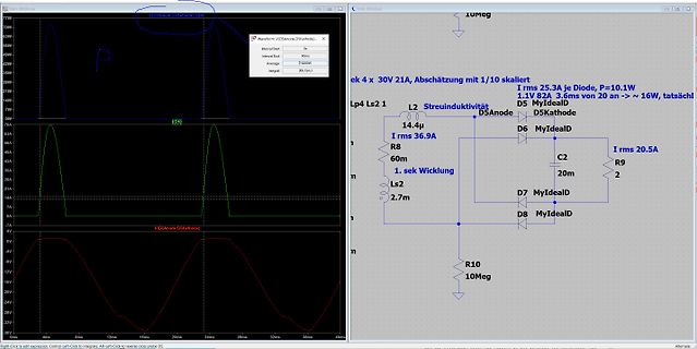
Schaltplan und Oszilloskop-Messungen einer Schaltung
, Abschätzung mit 1/10 skaliert I rms 25.3A je Diode, P=10.1W Lp4 Ls2 1 L2 Streuinduktivität D5 MyIdealD D5Kathode D6 MyIdealD I rms 36.9A R8 60m 1. sek Wicklung C2 20m Ls2 2.7m R9 2 I rms 20.5A D7 MyIdealD D8 MyIdealD R10 10Meg
in „Messen von Dioden mit Multimeter“ · Analoge Elektronik und Schaltungstechnik · · Screenshots
-
PDF
db883bb7785064c5f8a8b3b8f50858ea45a7.pdf
forward. These MathCAD results provided a starting point for initial design values. However, It assumes ideal components, All capacitors are low ESR porcelain ceramic capacitors includes no parasitics, and assumes an ideal 50% duty- chosen for their low-loss RF characteristics. Note that the drain peak voltage
in „Bauplan für HF Netzteil gesucht.“ · HF, Funk und Felder ·
-
PDF
IKSdrehzahl_IL8190_datasheet.pdf
COS- Figure 3. Output Angle in Polar Form Figure 4. Nominal Output Deviation 45 40 35 30 25 20 15 Ideal Degrees 10 5 0 1 5 9 13 17 21 25 29 33 37 41 45 Nominall Angle (Degrees) Figure 5. Nominal Angle vs. Ideal Angle (After Calibrating at 180) December, 2012, Rev. 02 IL8190 Table 1. Function Generator Output Nominal Angle vs. Ideal Angle (After Calibrating at 270) Nomi- Nomi- Nomi- Nomi- Nomi- Nomi- Ideal Ideal Ideal Ideal Ideal Ideal Degrees nal Degrees nal Degrees nal Degrees nal Degrees nal Degrees nal Degrees Degrees Degrees
in „Brauche Hilfe bei der Suche nach einem IC. Bin kein Fachmann.“ · Fahrzeugelektronik ·
-
PDF
Musterseite.pdf
▯ ▯▯▯▯▯ ▯▯▯▯▯ ▯▯ ▯▯▯▯▯▯▯▯▯▯ ▯ Träge Masse - Translation (ideale Kapazität) 1 Das ideale mechanische Bauelement träge Masse speichert als ideale Kapazität nur P- Energie. Da die Kapazität selbst keine dissipativen Eigenschaften besitzt, beinhaltet sie auch keine Leistungsverluste in Form von Prozessleistung. Das Ersatzschaltbild der idealen Kapazität enthält deshalb – keine Induktivität – einen Serienwiderstand von ▯ ▯ ▯ ▯ – einen Parallelwiderstand von ▯ ▯ ▯ ▯. Tab. 2.1: mechatronische Kapazität – träge Masse ▯▯▯▯▯ ▯ ▯▯▯▯ ▯ ▯▯▯ ▯▯▯
in „Open Office vs. MS Office für (Abschluss)Arbeit“ · Offtopic ·
-
PDF
ATmega8-ADC.pdf
read as 0, and the highest code is read as 2 -1. Several parameters describe the deviation from the ideal behavior: Offset: The deviation of the first transition (0x000 to 0x001) compared to the ideal transition (at 0.5 LSB). Ideal value: 0 LSB. Figure 97. Offset Error Output Code Ideal ADC Actual ADC
in „Frage zur Beschaltung“ · Mikrocontroller und Digitale Elektronik ·
-
PDF
Antennen_Wellenausbreitung_Folie_DJ3BO_November2013.pdf
Aufstellung 5 m über ideal leitfähigem Boden Aufstellung 10 m über ideal leitfähigem Boden (Kupferverluste vernachlässigt) (Kupferverluste vernachlässigt) Vortrag > Autor > Dokumentname > 09.11.2005 Antenne: Beam mit unterschiedlicher