Hi

Ich habe jetzt mehr oder weniger ein DDR2 Model von Micron zum laufen
gebracht habe jetzt 2. Probleme.

1. Kommt beim Schreiben und Lesen nur 'X' rein bzw. raus.
(Beim Schreiben sagen mir das die Nachrichten von Model und beim Lesen
kommt halt nur ein 'X' beim Lesen wobei die Strobe Signale gut
aussehen!)

2. Werden iwan alle Signale zu 'X' auch die, die nur von meinem
Controller zugewiesen werden.

Hat vllt. iwer Erfahrungen mit dem Micron Model und kann mir vllt.
weiter Helfen ?

Gruß Johny

PS: Das Model ist übrigens in Verilog und mein Controller in VHDL, als
Simulator benutze ich den ISim von Xilinx!
Angehängte Dateien:
-

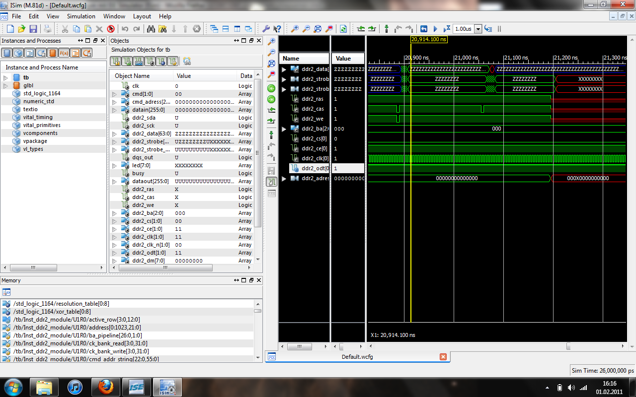
Sim.png
190 KB
Ich habe davon auch nicht so den Plan (nutze Quartus), aber hast du auch
beachtet, dass das DDR2-RAM auch initialisiert werden muss und dies ggf
mit simuliert wird? D.h. es braucht einige Zeit, bis es bereit ist (kann
im us-Bereich liegen, => länger simulieren und mit dem Schreiben
warten). Evtl kannst du die Initialisierung abschalten (ist bei Quartus
möglich)

Ich hoffe, dass ich Dir helfen konnte...
Johny,

mit den Micron Verilog Modellen kannst Du meistens einen DEBUG Pragma
setzen. Es muesste dann eine Fehlermeldung geben falls irgendwas mit der
Timing /Initialisierung nicht in Ordnung ist.

Letztes Jahr irgendwann hatte ich ein Micron Exemplar mit einem Lattice
DDR2 Controller/[active-hdl | riviera] Simulator laufen. Ich musste es
wieder ausgraben falls das Debug Fenster keine Geheimnisse verrät.

Grüße,
Charles


P.S.
Hier meine Verilog Timing Set-Up 'ddr_parameters.vh 'Datei, die ich
zufällig dabei habe.

`ifdef sg5B                               //              Timing
Parameters for -5B (CL = 3)
    parameter tCK              =     5.0; // tCK    ns    Nominal Clock
Cycle Time
    parameter tDQSQ            =     0.4; // tDQSQ  ns    DQS-DQ skew,
DQS to last DQ valid, per group, per access
    parameter tMRD             =    10.0; // tMRD   ns    Load Mode
Register command cycle time
    parameter tRAP             =    15.0; // tRAP   ns    ACTIVE to READ
with Auto precharge command
    parameter tRAS             =    40.0; // tRAS   ns    Active to
Precharge command time
    parameter tRC              =    55.0; // tRC    ns    Active to
Active/Auto Refresh command time
    parameter tRFC             =    70.0; // tRFC   ns    Refresh to
Refresh Command interval time
    parameter tRCD             =    15.0; // tRCD   ns    Active to
Read/Write command time
    parameter tRP              =    15.0; // tRP    ns    Precharge
command period
    parameter tRRD             =    10.0; // tRRD   ns    Active bank a
to Active bank b command time
    parameter tWR              =    15.0; // tWR    ns    Write recovery
time
`else `ifdef sg6T                         //              Timing
Parameters for -6T (CL = 2.5)
    parameter tCK              =     6.0; // tCK    ns    Nominal Clock
Cycle Time
    parameter tDQSQ            =    0.45; // tDQSQ  ns    DQS-DQ skew,
DQS to last DQ valid, per group, per access
    parameter tMRD             =    12.0; // tMRD   ns    Load Mode
Register command cycle time
    parameter tRAP             =    15.0; // tRAP   ns    ACTIVE to READ
with Auto precharge command
    parameter tRAS             =    42.0; // tRAS   ns    Active to
Precharge command time
    parameter tRC              =    60.0; // tRC    ns    Active to
Active/Auto Refresh command time
    parameter tRFC             =    72.0; // tRFC   ns    Refresh to
Refresh Command interval time
    parameter tRCD             =    15.0; // tRCD   ns    Active to
Read/Write command time
    parameter tRP              =    15.0; // tRP    ns    Precharge
command period
    parameter tRRD             =    12.0; // tRRD   ns    Active bank a
to Active bank b command time
    parameter tWR              =    15.0; // tWR    ns    Write recovery
time
`else `ifdef sg6                          //              Timing
Parameters for -6 (CL = 2.5)
    parameter tCK              =     6.0; // tCK    ns    Nominal Clock
Cycle Time
    parameter tDQSQ            =     0.4; // tDQSQ  ns    DQS-DQ skew,
DQS to last DQ valid, per group, per access
    parameter tMRD             =    12.0; // tMRD   ns    Load Mode
Register command cycle time
    parameter tRAP             =    15.0; // tRAP   ns    ACTIVE to READ
with Auto precharge command
    parameter tRAS             =    42.0; // tRAS   ns    Active to
Precharge command time
    parameter tRC              =    60.0; // tRC    ns    Active to
Active/Auto Refresh command time
    parameter tRFC             =    72.0; // tRFC   ns    Refresh to
Refresh Command interval time
    parameter tRCD             =    15.0; // tRCD   ns    Active to
Read/Write command time
    parameter tRP              =    15.0; // tRP    ns    Precharge
command period
    parameter tRRD             =    12.0; // tRRD   ns    Active bank a
to Active bank b command time
    parameter tWR              =    15.0; // tWR    ns    Write recovery
time
`else `ifdef sg75E                        //              Timing
Parameters for -75E (CL = 2)
    parameter tCK              =     7.5; // tCK    ns    Nominal Clock
Cycle Time
    parameter tDQSQ            =     0.5; // tDQSQ  ns    DQS-DQ skew,
DQS to last DQ valid, per group, per access
    parameter tMRD             =    15.0; // tMRD   ns    Load Mode
Register command cycle time
    parameter tRAP             =    15.0; // tRAP   ns    ACTIVE to READ
with Auto precharge command
    parameter tRAS             =    40.0; // tRAS   ns    Active to
Precharge command time
    parameter tRC              =    60.0; // tRC    ns    Active to
Active/Auto Refresh command time
    parameter tRFC             =    75.0; // tRFC   ns    Refresh to
Refresh Command interval time
    parameter tRCD             =    15.0; // tRCD   ns    Active to
Read/Write command time
    parameter tRP              =    15.0; // tRP    ns    Precharge
command period
    parameter tRRD             =    15.0; // tRRD   ns    Active bank a
to Active bank b command time
    parameter tWR              =    15.0; // tWR    ns    Write recovery
time
`else `ifdef sg75Z                        //              Timing
Parameters for -75Z (CL = 2)
    parameter tCK              =     7.5; // tCK    ns    Nominal Clock
Cycle Time
    parameter tDQSQ            =     0.5; // tDQSQ  ns    DQS-DQ skew,
DQS to last DQ valid, per group, per access
    parameter tMRD             =    15.0; // tMRD   ns    Load Mode
Register command cycle time
    parameter tRAP             =    20.0; // tRAP   ns    ACTIVE to READ
with Auto precharge command
    parameter tRAS             =    40.0; // tRAS   ns    Active to
Precharge command time
    parameter tRC              =    65.0; // tRC    ns    Active to
Active/Auto Refresh command time
    parameter tRFC             =    75.0; // tRFC   ns    Refresh to
Refresh Command interval time
    parameter tRCD             =    20.0; // tRCD   ns    Active to
Read/Write command time
    parameter tRP              =    20.0; // tRP    ns    Precharge
command period
    parameter tRRD             =    15.0; // tRRD   ns    Active bank a
to Active bank b command time
    parameter tWR              =    15.0; // tWR    ns    Write recovery
time
`else `define sg75                        //              Timing
Parameters for -75 (CL = 2.5)
    parameter tCK              =     7.5; // tCK    ns    Nominal Clock
Cycle Time
    parameter tDQSQ            =     0.5; // tDQSQ  ns    DQS-DQ skew,
DQS to last DQ valid, per group, per access
    parameter tMRD             =    15.0; // tMRD   ns    Load Mode
Register command cycle time
    parameter tRAP             =    20.0; // tRAP   ns    ACTIVE to READ
with Auto precharge command
    parameter tRAS             =    40.0; // tRAS   ns    Active to
Precharge command time
    parameter tRC              =    65.0; // tRC    ns    Active to
Active/Auto Refresh command time
    parameter tRFC             =    75.0; // tRFC   ns    Refresh to
Refresh Command interval time
    parameter tRCD             =    20.0; // tRCD   ns    Active to
Read/Write command time
    parameter tRP              =    20.0; // tRP    ns    Precharge
command period
    parameter tRRD             =    15.0; // tRRD   ns    Active bank a
to Active bank b command time
    parameter tWR              =    15.0; // tWR    ns    Write recovery
time
`endif `endif `endif `endif `endif

    // Size Parameters based on Part Width

`ifdef x4
    parameter ADDR_BITS        =      13; // Set this parameter to
control how many Address bits are used
    parameter DQ_BITS          =       4; // Set this parameter to
control how many Data bits are used
    parameter DQS_BITS         =       1; // Set this parameter to
control how many DQS bits are used
    parameter DM_BITS          =       1; // Set this parameter to
control how many DM bits are used
    parameter COL_BITS         =      11; // Set this parameter to
control how many Column bits are used
`else `ifdef x8
    parameter ADDR_BITS        =      13; // Set this parameter to
control how many Address bits are used
    parameter DQ_BITS          =       8; // Set this parameter to
control how many Data bits are used
    parameter DQS_BITS         =       1; // Set this parameter to
control how many DQS bits are used
    parameter DM_BITS          =       1; // Set this parameter to
control how many DM bits are used
    parameter COL_BITS         =      10; // Set this parameter to
control how many Column bits are used
`else `define x16
    parameter ADDR_BITS        =      13; // Set this parameter to
control how many Address bits are used
    parameter DQ_BITS          =      16; // Set this parameter to
control how many Data bits are used
    parameter DQS_BITS         =       2; // Set this parameter to
control how many DQS bits are used
    parameter DM_BITS          =       2; // Set this parameter to
control how many DM bits are used
    parameter COL_BITS         =       9; // Set this parameter to
control how many Column bits are used
`endif `endif

    parameter BA_BITS          =       2; // Set this parmaeter to
control how many Bank Address bits are used
    parameter full_mem_bits    = BA_BITS+ADDR_BITS+COL_BITS; // Set this
parameter to control how many unique addresses are used
    parameter part_mem_bits    = 10;                   // Set this
parameter to control how many unique addresses are used

    parameter no_halt          =       1; // If set to 1, the model
won't halt on command sequence/major errors

`ifdef MEM_DEBUG
    parameter DEBUG            =       1; // Turn on DEBUG message
`else
    parameter DEBUG            =       0; // Turn on DEBUG message
`endif
Hi

So habe mal mit Initialisiert (bzw. mit die 200 µs gewartet da ich das
sonst für die Simulation abgeschaltet habe!)
Doch das Problem ist immer noch das selbe, Definiere auch alle Timings
usw. per --Define also das passt denke ich, doch das mit den X ist halt
merkwürdig da es auch die CAS, RAS und WE Leitung betrifft die ja
wirklich nur von mir beschrieben werden!

Falls noch jemand iwie ne Idee hat immer her damit :)

Gruß Johny
Johny schrieb:

> PS: Das Model ist übrigens in Verilog und mein Controller in VHDL, als
> Simulator benutze ich den ISim von Xilinx!

Autsch! Früher ging sowas soweit ich weiß nur mit ModelSim! Falls das
inzwischen auch mit ISIM gehen sollte, wäre mir ganz neu.
ISim kann schon lange Mixed Language Simulation:
http://www.xilinx.com/itp/xilinx10/isehelp/ism_c_overview.htm
Christian R. schrieb:
> ISim kann schon lange Mixed Language Simulation:
> http://www.xilinx.com/itp/xilinx10/isehelp/ism_c_overview.htm

Das weiß ich, aber irgendwo hatte ich mal gelesen, dass sich der MIG nur
mit ModelSim simulieren lässt. Kann natürlich sein, dass das nicht mehr
der Fall ist.
Johny schrieb:
> So habe mal mit Initialisiert (bzw. mit die 200 µs gewartet da ich das
Gute Idee.

> Doch das Problem ist immer noch das selbe, Definiere auch alle Timings
> usw. per --Define also das passt denke ich, doch das mit den X ist halt
> merkwürdig da es auch die CAS, RAS und WE Leitung betrifft die ja
> wirklich nur von mir beschrieben werden!
Offenbar nicht. Die Xe würde ich mir mal genau angucken.

Außerdem hast Du in Deinem Logfile auch einige Fehlermeldungen (nach den
SDF-Meldungen):
1 | tb.Inst_ddr2_module.U1R0.cmd_task: at time 204037600.0 ps ERROR: Load Mode 0 Illegal Burst Length = 1 |
2 | tb.Inst_ddr2_module.U1R0.cmd_task: at time 204037600.0 ps ERROR: Load Mode 0 Illegal CAS Latency = 0 |
3 | tb.Inst_ddr2_module.U1R0.main: at time 205037600.0 ps ERROR: CAS Latency = 0 is illegal @tCK(avg) = 5000.000000 |
4 | tb.Inst_ddr2_module.U1R0.main: at time 205037600.0 ps ERROR: Write Recovery = 1 is illegal @tCK(avg) = 5000.000000 |
5 | tb.Inst_ddr2_module.U2R0.main: at time 205037600.0 ps ERROR: CAS Latency = 0 is illegal @tCK(avg) = 5000.000000 |
6 | tb.Inst_ddr2_module.U2R0.main: at time 205037600.0 ps ERROR: Write Recovery = 1 is illegal @tCK(avg) = 5000.000000 |
7 | tb.Inst_ddr2_module.U4R0.main: at time 205037600.0 ps ERROR: CAS Latency = 0 is illegal @tCK(avg) = 5000.000000 |
8 | tb.Inst_ddr2_module.U4R0.main: at time 205037600.0 ps ERROR: Write Recovery = 1 is illegal @tCK(avg) = 5000.000000 |
9 | tb.Inst_ddr2_module.U5R0.main: at time 205037600.0 ps ERROR: CAS Latency = 0 is illegal @tCK(avg) = 5000.000000 |
10 | tb.Inst_ddr2_module.U5R0.main: at time 205037600.0 ps ERROR: Write Recovery = 1 is illegal @tCK(avg) = 5000.000000 |
11 | tb.Inst_ddr2_module.U1R0.data_task: at time 220907600.0 ps ERROR: tDSS violation on DQS bit 0 |
12 | tb.Inst_ddr2_module.U1R0.data_task: at time 220907600.0 ps ERROR: tDSS violation on DQS bit 1 |
13 | tb.Inst_ddr2_module.U1R0.data_task: at time 220907600.0 ps ERROR: tDSS violation on DQS_N bit 0 |
14 | tb.Inst_ddr2_module.U1R0.data_task: at time 220907600.0 ps ERROR: tDSS violation on DQS_N bit 1 |
Duke
So

Das Problem gefunden:

Bei dem Micron Model waren fertige Pakete für SODIMS usw. mit dabei!
Bei denen wurden aber die DM Bits nicht mit "durch geschleift".

Intern werden iwelche Logichen Operatoren mit den DM und DQ Bits
veranstaltet und X OR 0 oa. ergibt halt immer X :-/

Ärgerlich aber falls jemand den Thread findet hat er direkt ne Lösung!

Gruß Max
Bitte melde dich an um einen Beitrag zu schreiben. Anmeldung ist kostenlos und dauert nur eine Minute.
Bestehender Account
Schon ein Account bei Google/GoogleMail? Keine Anmeldung erforderlich!
Mit Google-Account einloggen
Mit Google-Account einloggen
Noch kein Account? Hier anmelden.