Hallo.

Nachdem ich festgestellt habe, dass die "russische" CMOS-Logik sehr viel
Rechenleistung frisst, wollte ich es mal mit einem Behavioral
AND-Baustein versuchen, der im Component-Selektor im Unterordner
[Digital] zu finden ist. Das Gatter hat 5 Eingänge (a,b,c,d,e,f), einen
Q-Anschluss als nicht invertierter Ausgang, einen Qi-Anschluss als
invertierenden Ausgang und einen "com"-Anschluss, dessen Bedeutung sich
mir verschließt.

Ich habe den "com"-Anschluss schon mal versuchsweise auf 0 bzw auf Vdd
gelegt und auch offen betrieben, egal was ich mache, ich bringe kein
Ergebnis zustande! Kann mir jemand einen Tip geben?
Angehängte Dateien:
-

Attributes.PNG
3,6 KB -

Digital_A_Devices.asc.PNG
22 KB
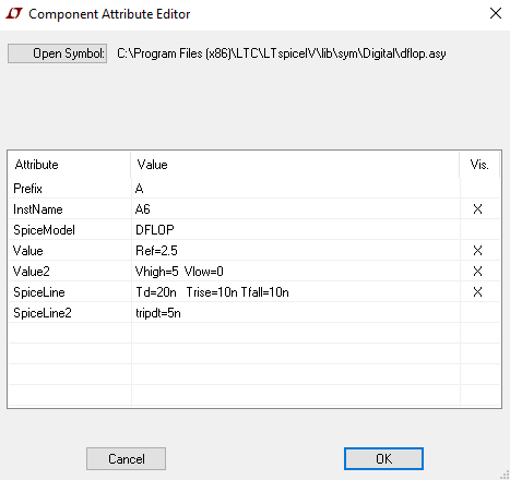
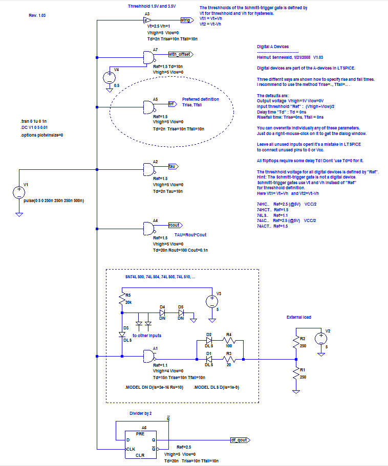
Hallo,

1.
Unbenutzte Eingänge offen lassen damit LTspice die wegoptimieren kann.
2.
Rechter Mausklick auf das Symbol offnet ein Dialogfenster um Parameter
einzugeben.

REF=2.5 VHIGH=5 VLOW=0
TD=5n TRISE=5n

Die Simulationsdatei(.asc) für LTspice ist im Anhang.

Gruß
Helmut
Hallo Helmut.

Müsste ich diese Informationen zu den Parametern nicht irgendwo in der
mitgelieferten LTspice-Doku finden?

Entsprechend A5 in DIGITAL_A_DEVICES_1.ASC soll für "Ref" der Wert von
1.5 vorgesehen werden - aber

Input threshhold "Ref" :  (Vhigh+Vlow)/2 - aber:

Jetzt finde ich für den CD4011 bei Vdd=15V die Werte V_IL=6V V_IH=9V -
alles typisch bei 25°C.

Liege ich richtig mit den Annahmen V_IH -> Vhigh und V_IL -> Vlow? Dann
wäre Ref=7.5V?

Laut Fairchild (alle Werte bei Vdd=15V):
Propagation Delay Time, HIGH-to-LOW Level, tPHL=35n
Propagation Delay Time, LOW-to-HIGH Level, tPLH=30n
Transition Time, tTHL, tTLH =40n

daraus folgt:
tTLH -> Trise?
tTHL -> Tfall?
max(tPHL, tPLH) -> Td?

Danke für die Informationen.

LG
Angehängte Dateien:
-

A-help.PNG
38 KB
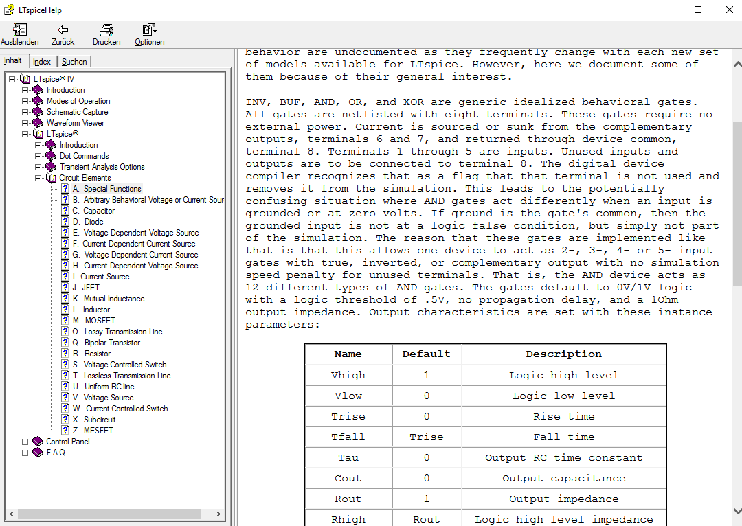
> Hallo Helmut.

> Müsste ich diese Informationen zu den Parametern nicht irgendwo in der
mitgelieferten LTspice-Doku finden?

Die ist in der Help von LTspice. Siehe Anhang
Weiterführende Help über A-devices gibt es hier.
http://ltwiki.org/?title=Undocumented_LTspice#A-Devices


> Entsprechend A5 in DIGITAL_A_DEVICES_1.ASC soll für "Ref" der Wert von
1.5 vorgesehen werden - aber

> Input threshhold "Ref" :  (Vhigh+Vlow)/2 - aber:

Wenn man "Ref" nicht angibt, dann gilt obige Formel für Ref.


> Jetzt finde ich für den CD4011 bei Vdd=15V die Werte V_IL=6V V_IH=9V -
alles typisch bei 25°C.

> Liege ich richtig mit den Annahmen V_IH -> Vhigh und V_IL -> Vlow? Dann
wäre Ref=7.5V?

Ja.

Vhigh=15 Vlow=0


> Laut Fairchild (alle Werte bei Vdd=15V):
> Propagation Delay Time, HIGH-to-LOW Level, tPHL=35n
> Propagation Delay Time, LOW-to-HIGH Level, tPLH=30n
> Transition Time, tTHL, tTLH =40n

daraus folgt:
tTLH -> Trise? Ja
tTHL -> Tfall? Ja
max(tPHL, tPLH) -> Td? Ja


--- Anhang ---

A. Special Functions
Symbol names: INV, BUF, AND, OR, XOR, SCHMITT, SCHMTBUF, SCHMTINV,
DFLOP, VARISTOR, and MODULATE

Syntax: Annn n001 n002 n003 n004 n005 n006 n007 n008 <model> [instance
parameters]

These are Linear Technology Corporation's proprietary special
function/mixed mode simulation devices. Most of these and their behavior
are undocumented as they frequently change with each new set of models
available for LTspice. However, here we document some of them because of
their general interest.

INV, BUF, AND, OR, and XOR are generic idealized behavioral gates. All
gates are netlisted with eight terminals. These gates require no
external power. Current is sourced or sunk from the complementary
outputs, terminals 6 and 7, and returned through device common, terminal
8. Terminals 1 through 5 are inputs. Unused inputs and outputs are to be
connected to terminal 8. The digital device compiler recognizes that as
a flag that that terminal is not used and removes it from the
simulation. This leads to the potentially confusing situation where AND
gates act differently when an input is grounded or at zero volts. If
ground is the gate's common, then the grounded input is not at a logic
false condition, but simply not part of the simulation. The reason that
these gates are implemented like that is that this allows one device to
act as 2-, 3-, 4- or 5- input gates with true, inverted, or
complementary output with no simulation speed penalty for unused
terminals. That is, the AND device acts as 12 different types of AND
gates. The gates default to 0V/1V logic with a logic threshold of .5V,
no propagation delay, and a 1Ohm output impedance. Output
characteristics are set with these instance parameters:

Name Default Description
Vhigh 1  Logic high level
Vlow  0  Logic low level
Trise 0  Rise time
Tfall Trise Fall time
Tau  0  Output RC time constant
Cout  0  Output capacitance
Rout  1  Output impedance
Rhigh Rout  Logic high level impedance
Rlow  Rout  Logic low level impedance

Note that not all parameters can be specified on the same instance at
the same time, e.g., the output characteristics are either a slewing
rise time or an RC time constant, not both.

The propagation delay defaults to zero and is set with instance
parameter Td. Input hold time is equal to the propagation delay.

The input logic threshold defaults to .5*(Vhigh+Vlow) but can be set
with the instance parameter Ref. The hold time is equal to the
propagation delay.

The exclusive XOR device has non-standard behavior when more than two
inputs are used: The output is true only when exactly one of all inputs
is true. Use the associative property of XOR's with multiple XOR devices
to implement an XOR block with more than two inputs.

The Schmitt trigger devices have similar output characteristics as the
gates. Their trip points are specified with instance parameters Vt and
Vh. The low trip point is Vt-Vh and the high trip point is Vt+Vh.

The gates and Schmitt trigger devices supply no timestep information to
the simulation engine by default. That is, they don't look when they are
about to change state and make sure there's a timestep close to either
side of the state change. The instance parameter tripdt can be set to
stipulate a maximum timestep size the simulator takes across state
changes.

The VARISTOR is a voltage controlled varistor. Its breakdown voltage is
set by the voltage between terminals 1 and 2. Its breakdown impedance is
specified with the instance parameter rclamp. See the example schematic
.\examples\Educational\varistor.asc

The MODULATE device is a voltage controlled oscillator. See the example
schematic .\examples\Educational\PLL.asc. The instantaneous oscillation
frequency is set by the voltage on the FM input. The conversion from
voltage to frequency is linear and set by the two instance parameters,
mark and space. Mark is the frequency when the FM input is at 1V and
space is the frequency when the input is at 0V. The amplitude is set by
the voltage on the AM input and defaults to 1V if that input is
unused(connected to the MODULATE common).

The schematic capture aspect of LTspice netlists symbols for these
devices in a special manner. All unconnected terminals are automatically
connected to terminal 8. Also, if terminal 8 is unconnected, then it is
connected to node 0.
Hallo Helmut.

Ich danke Dir noch einmal für Deine Hilfe. Die Mächtigkeit dieses
Werkzeuges überblicke ich erst so nach und nach.

Auf jeden Fall habe ich den Eindruck, das die Build-In-Logik (?) weniger
Rechenzeit benötigt als die Symbole aus der "russischen" Bibliothek.

Ich bin jetzt mit meinem Vorhaben ein ganzes Stück weiter gekommen, da
die Erfolge somit in greifbare Nähe gerückt sind.
Ja die originalen A-devices benötigen immer viel weniger Rechenzeit als
drumherum gebaute Subcircuits.
Helmut S. schrieb:
> Ja die originalen A-devices benötigen immer viel weniger Rechenzeit als
> drumherum gebaute Subcircuits.

Nachtrag

In der LTspice Yahoo group gibt es auch Libraries für CD4000 und
74HC/74HCT im Verzeichnis Lib. Es ist zwar manchmal bequem die zu
nehmen, aber wenn man  nur ein Gatter braucht schleppt man unnötig
Ballast mit. Diese Libraries hatte ich vor 10 Jahren für die Yahoo group
geschrieben.
Angehängte Dateien:
-

Liftcontroller.png
270 KB
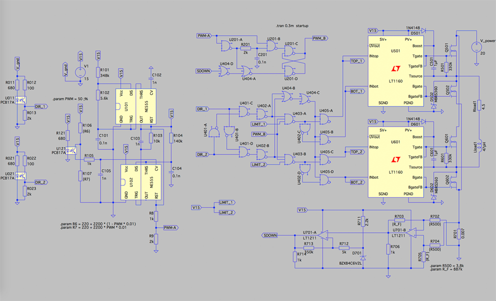
Vor 10 Jahren hatte ich mit Spice noch nix am Hut. Für Spice hat sich
mein Interesse erst zum Jahresende 2015 entwickelt.

Ich habe jetzt in einem PWM-Modul (siehe angehängtes Bildschirmfoto)
alle "russischen Gatter" gegen A-Devices getauscht. Die Berechnungszeit
hat sich dadurch drastisch auf weniger als 30% der ursprünglichen
verkürzt. Die Entwicklung ist noch nicht abgeschlossen, das war auch der
Antrieb darauf zu achten, die Berechnungszeiten nicht unnötig
aufzublähen. Vieles könnte man auch mit höher integrierten ICs
realisieren. Mir kommt es aber auf die Störfestigkeit in einer rauhen
Umgebung an. Deshalb habe ich mich auf eine höhere Versorgungsspannung
festgelegt.
@Flash,
danke für deinen Erfahrungsbericht und den Schaltplan.

Vermutlich war ja deine "russische" Lib die CD4000.lib von der Yahoo
group. Das macht aber nichts. Hauptsache die Leute sind von LTspice und
der Unterstüzung durch andere Benutzer begeistert.

Gruß
Helmut
Angehängte Dateien:
-

Gated_Trigger.png
59 KB
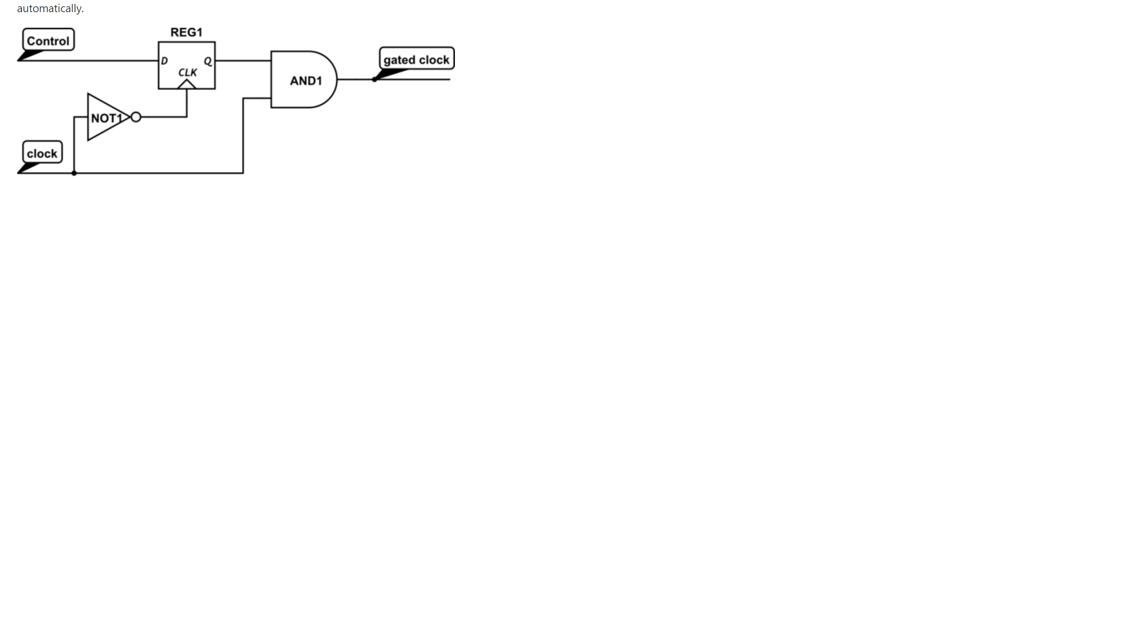
Ich habe mich für diese Variante entschieden. Ich invertiere den Clock
mit Hilfe eines Inverters somit tastet der FF das Signal mit der
fallenden Flanke ab. Den Output Buffer mit den Enable Pin habe ich durch
ein UND Gatter mit 2 Eingängen ersetzt. Vielen Dank für die Hilfe das
hat mir wirklich weiter geholfen.
Bitte melde dich an um einen Beitrag zu schreiben. Anmeldung ist kostenlos und dauert nur eine Minute.
Bestehender Account
Schon ein Account bei Google/GoogleMail? Keine Anmeldung erforderlich!
Mit Google-Account einloggen
Mit Google-Account einloggen
Noch kein Account? Hier anmelden.