Hallo Leute!

Ich durchblicke die Bezeichnung der Timer Register/Interrupt Vector
nicht ganz.

Momentan beginne ich wieder mich in die ganze Programmierung
einzuarbeiten und versuche mich an kleinen Testbsp.

z.B. folgendes (Kombination aus Vorlage und Selbsterstelltem)
1 | #include <msp430.h>
|
2 |
|
3 | volatile int unsigned time;
|
4 | volatile int wert=25000;
|
5 |
|
6 | int main(void)
|
7 | {
|
8 | WDTCTL = WDTPW + WDTHOLD; // Stop WDT
|
9 |
|
10 | BCSCTL1 = CALBC1_1MHZ; // DCO at 1 MHz
|
11 | DCOCTL = CALDCO_1MHZ; // DCO at 1 MHz
|
12 |
|
13 | BCSCTL2 = DIVM_3 + DIVS_3;
|
14 | // Divider for MCL and SMCLK _1 --> /2; _2 -->/4; _3-->/8
|
15 | // SMCLK: 125kHz MCLK= 125kHz
|
16 |
|
17 | P1DIR |= BIT2; // P1.2 output
|
18 | P1SEL |= BIT2; // P1.2 for TA0.1 output
|
19 | P1SEL2 = 0; // Select default function for P1.2
|
20 | TA0CTL = TASSEL_2 + MC_1; // SMCLK as source for Timer 0, Up mode: the timer counts up to TACCR0,
|
21 | TA0CCTL1 = OUTMOD_2 + CM_1 ; // CCR0 toogle/set
|
22 | TA0CCR0 = 65536-1; // PWM Period for Timer 0 and Capture and Compare register 0
|
23 | TA0CCR1 = wert; //~0,25s // CCR1 PWM duty cycle
|
24 |
|
25 | //measure
|
26 | P2DIR |= 0x00; // Port 2 as inputs
|
27 | P2SEL |= BIT5; // select Capture function on P2.5
|
28 | P2SEL |= 0x02;
|
29 | P2SEL2 = 0x00;
|
30 |
|
31 | TA1CTL = TASSEL_2 + MC_2; // SMCLK, continuous mode up to 0xffff
|
32 | TA1CCTL1 = CM_1 + CCIS_0 + SCS + CAP + CCIE;
|
33 | //capture on rising edge, CCIxB, Synchronous capture, capture mode,Interrupt enabled
|
34 |
|
35 |
|
36 | __bis_SR_register( GIE); // Enter LPM0
|
37 | }
|
38 |
|
39 | #pragma vector = TIMER1_A1_VECTOR
|
40 | __interrupt void Timer1_A1_ISR(void) {
|
41 | switch(TA1IV) {
|
42 | case 2: time = TA1CCR1; // stopTime auslesen
|
43 |
|
44 | break;
|
45 | case 4:
|
46 | case 10: break;
|
47 | }
|
48 | }
|
Das Programm funktioniert soweit, bis auf das falsche Messergebnis aber
dass muss ich mir erst ansehen. Ich will einfach eine PWM an einem Port
ausgeben und an einem anderen "messen".
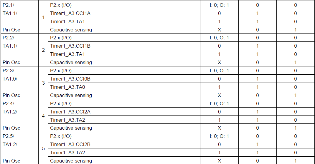
Nun möchte ich als Input-Pin P2.5 anstatt P2.1 nehmen und daran
scheitere ich. Im Datenblatt steht bei P2.5 CCI2B statt CCI1A.
Das kann ich ja über CCIS bei TA1CCTL1 einstellen.
Was sagt der 2er aus? 2. Register? Muss ich dann TA1CCTL2 nehmen?
Und was bezeichnet das A1 beim Interrupt vector? --> TA1CCTL1?
Danke!
--
Bitte die [ c ] [ /c ]-Tags für Sourcecode verwenden.
-rufus