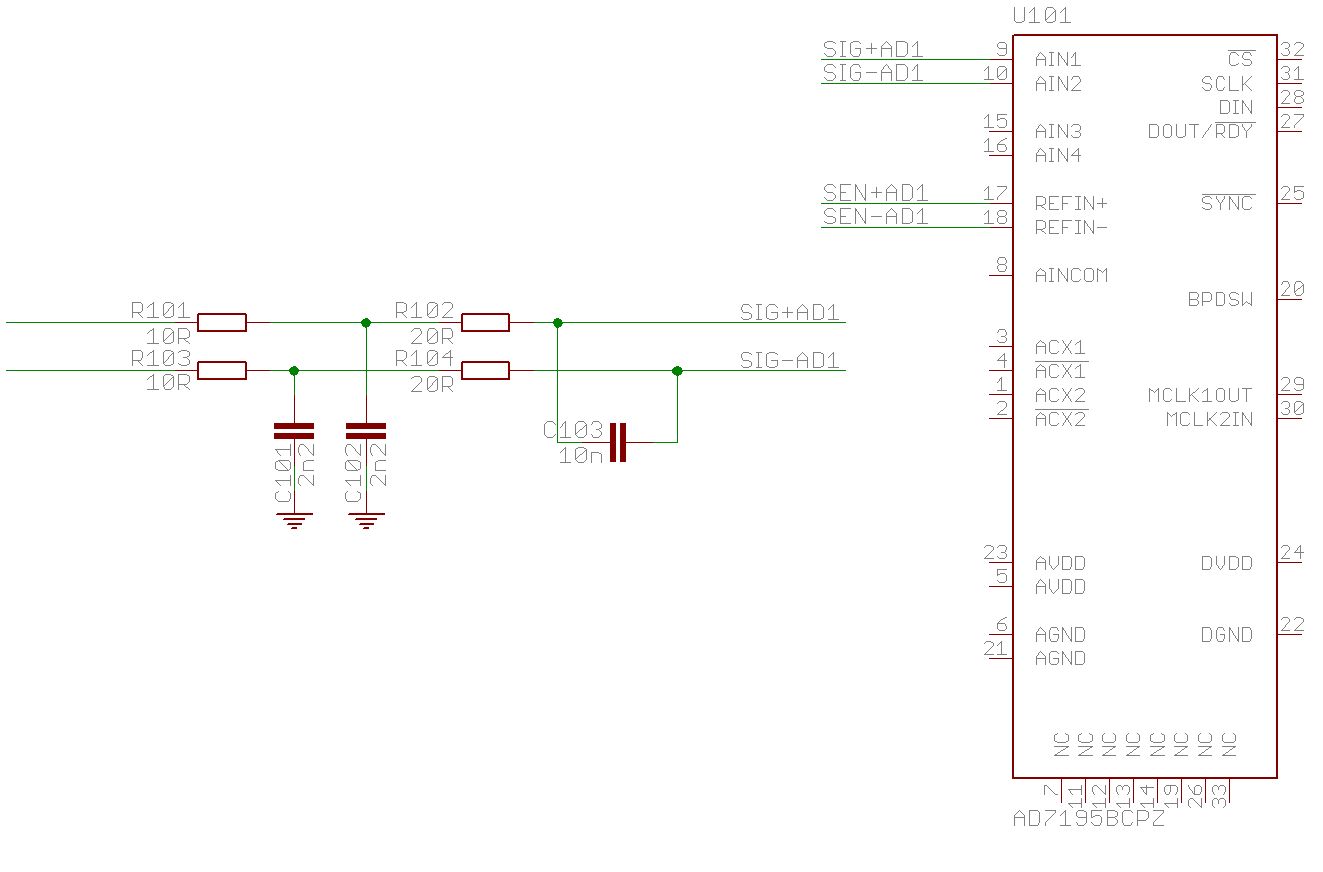
Hallo Zusammen,
ich entwerfe gerade eine Baugruppe mit einem
AD7195 24-Bit Sigma-Delta ADC
http://www.analog.com/en/products/analog-to-digital-converters/ad-converters/ad7195.html

Die Signalquelle hat 700R Impedanz und soll auf der Baugruppe die
skizzierte Filterstruktur durchlaufen.
Zugunsten einer größeren Gleichtaktaussteuerung wird der ADC ohne
Eingangspuffer betrieben (unbuffered).

Bisher bin ich der Meinung, dass dieses Filter dem Sample-Kondensator
niederimpedant einen Ladungsvorrat zur Verfügung stellt.

Nun steht in der Doku:

<FAQ>
-> FAQ
The data sheet mentions that large external capacitors between the input
and ground can affect measurement accuracy in unbuffered mode. Can you
explain why this is the case? Does it only affect ac input signals, or
are dc input signals affected, too?
If you use the ADC in unbuffered mode, large RC constants on the input
can interact with the internal sampling capacitor and effectively starve
the sampling cap of charging current. This will cause gain errors in the
ADC.
The solution is either to use buffered mode or ensure that you respect
the maximum RC values given in the data sheet.
The reference inputs are also unbuffered so, as with using the analog
inputs in unbuffered mode, the RC loading on the reference inputs must
be sufficiently low to avoid introducing errors into the conversion
process.
</FAQ>

<DATASHEET> -> AD7195 datasheet
ANALOG INPUT CHANNEL
The AD7195 has two differential/four pseudo differential analog input
channels, which can be buffered or unbuffered. In buffered mode (the BUF
bit in the configuration register is set to 1), the input channel feeds
into a high impedance input stage of the buffer amplifier. Therefore,
the input can tolerate significant source impedances and is tailored for
direct connection to external resistive-type sensors such as strain
gages or resistance temperature detectors (RTDs).
When BUF = 0, the part operates in unbuffered mode. This results in a
higher analog input current. Note that this unbuffered input path
provides a dynamic load to the driving source.
Therefore, resistor/capacitor combinations on the input pins can cause
gain errors, depending on the output impedance of the source that is
driving the ADC input. Table 27 shows the allowable external
resistance/capacitance values for unbuffered mode at a gain of 1 such
that no gain error at the 20-bit level is introduced.
Table 27. External R-C Combination for No 20-Bit Gain Error
C (pF) R (Ω)
50     1.4 k
100    850
500    300
1000   230
5000   30
The absolute input voltage range in buffered mode is restricted to a
range between AGND + 250 mV and AVDD − 250 mV. Care must be taken in
setting up the common-mode voltage so that these limits are not
exceeded. Otherwise, linearity and noise performance degrades.
The absolute input voltage in unbuffered mode includes the range between
AGND − 50 mV and AVDD + 50 mV. The negative absolute input voltage limit
does allow the possibility of monitoring small true bipolar signals with
respect to AGND.
</DATASHEET>

Bei der vorliegenden Signalquelle wären 100pF das Limit.
Abgesehen davon, dass die Leitungskapazität im Bereich 25nF liegt, geht
mit nicht so recht in den Kopf, warum die zulässige Kapazität mit dem
Widerstand sinkt.

Leider fehlt mir für diesen Baustein die interne Struktur, so dass ich
die Strompfade im Eingangskreis, die zu dieser Problematik führen, nicht
nachvollziehen kann.

Ich habe bereits ADI angeschrieben, wollte aber mal rausfinden, ob hier
jemand zufällig dieses Thema kennt.

Danke Euch,
 marcus
Angehängte Dateien:
-

AD7195_Filters.gif
15 KB
Bitte melde dich an um einen Beitrag zu schreiben. Anmeldung ist kostenlos und dauert nur eine Minute.
Bestehender Account
Schon ein Account bei Google/GoogleMail? Keine Anmeldung erforderlich!
Mit Google-Account einloggen
Mit Google-Account einloggen
Noch kein Account? Hier anmelden.