A lookup table must be located at the same page to avoid getting wrong data. Thus, the lookup table has maximum 255 data for above example with starting a lookup table at X00h (X = 1, 2, 3, …, E, F). If a lookup table has fewer data, it needs
OUTPUT CURRENT 250mA OUTPUT CURRENT 300mA 100.0 100.0 95.0 95.0 90.0 90.0 ) 85.0 % ) 85.0 Y 80.0 ( C C E N 80.0 C 75.0 I F F 75.0 E 70.0 F E 65.0 70.0 60.0 65.0 55.0 60.0 1 2 3 4 5 6 7 8 9 10 11 1 2 3 4 5 6 7 8 9 10 11 LOADLED(S) LOADLED(S) VIN=24V VIN=48V VIN=24V VIN=48V OUTPUT CURRENT 350mA OUTPUT CURRENT 500mA 100.0 100.0 95.0 95.0 90.0 90.0 ) ) % 85.0 % 85.0 Y Y C 80.0 C 80.0 E I I I F 75.0 F 75.0 E E 70.0 70.0 65.0 65.0 60.0 60.0 1 2 3 4 5 6 7 8 9 10 11 1 2 3 4 5 6 7 8 9 10 11 LOADLED(S) LOADLED(S) VIN=24V VIN=48V VIN=24V VIN=48V OUTPUT CURRENT 700mA OUTPUT CURRENT 1000mA
probe tested on wafer at Tamb= +25°C Parameter Test Level Min Typ Max Unit Resolution IV 50 µm Size IV 8 x 280 Pixel Yield: number of bad pixels I 5 Bad pixels Equivalent resistance on TPP pin I 20 30 47 6 ® AT77C102B FingerChip 5364A–BIOM–11/03 ® AT77C102B FingerChip . Table 7. 3.3V Power supply The following
rather than being manually drawn. We now also have several integrated generators that produce both 3D model data and footprints from the same data definitions. Our median merge request processing time dropped from 3 days to 18 hours, despite receiving more merge requests than ever before (2105 new merge
integriert. Für die 3D-Tiefenerfassung das VL53L9CX dToF All-in-One LiDAR-Modul, Teil der ST FlightSense-Produktfamilie, das 3D-Tiefenerfassung mit präziser Reichweite bis zu 9 Metern bietet. Mit einer Auflösung von 54 x
R e 10 kΩ Mischsteilheit V M 3,8 S Empfindlichkeit U e für (S+N)/N = 6 dB 11 20 µV Interner Aufbau STB OSC MX01 MX02 14 9 3 4 V 5 P Strom- Anschlußbelegung versorgung Oszillator Mischer Vref8 2 MXI zögerungr
r 1 5 1 1 o x 8 t X X t - X l n 9 I b x c 3 T k e - 05 05 r 7 A 1 s 2 t x -x2436300 y 3 X a 4 2 2 e 0 M d 5 X k o 1 n E k a 3 2 5 1 2 X o D 1 o 0 1 X X 1 c S X b 0 ) N o - a E b k s 43 43 P ( d 1 e ) x -x1436300 S
TX- 9 7 D D D D 1 M X X X X X XXRXTO RCX X XTXT M C21 C22 8 L L L L I D D D D C CE E L S D D D D C 0.1uF 0.1uF L3 25MHz/49US MAGCOM_HS9024 D _ _ _ _ 2 2R 2 2 2 _ _ _ _ C27 C28 R4 R5 R6 R7 6 5 4 3 O 3 2 1 0 2 3 2 1 0 F.B/120
conditions. www.onsemi.com 4 MOC3081M, MOC3082M, MOC3083M TYPICAL PERFORMANCE CURVES 1.7 1.6 1.6 1.5 VTM = 3 V ) 1.5 NORMALIZED TO T A = 25_C ( 1.4 E 1.4 A L D1.3 O 1.3 T = −40_C I V A L R 1.2 M1.2 A TA = 25_C R W 1.1 O O ,1.1 F TA = 85_C I F 1.0 V 0.9 1.0 0.8 0.9 0.7 0.1 1 10 100 0.8 −40 −20 0 20 40 60 80
rich set of peripheral interfaces, including Gigabit Ethernet, USB 2.0 High-Speed Host/Device, SD 3.0/eMMC, CAN FD, Quad SPI, UART, I2C, I2S, PWM, and ADC. Developers can also accelerate evaluation and deployment of industrial edge and IIoT applications using the NuMaker-IoT-MA35D0-A2 (Chili Pro) Linux
feature in their firmware that restricts users from swapping RAM chips, sometimes even RAM chips of the same capacity from other Raspberry Pi boards. Daran merkt man halt, dass es um den Profit geht, und nichts anderes.
IDE, CubeMX). * Complete `main.c` code example. * Explanation of key parts. * Reminder about CubeMX. 8. **Self-Correction/Safety:** * Wait, did I miss something? The user repeated the exact same prompt three times. This might be a system glitch or the user didn't see the answer. I should answer it confidently
(mA) IC, COLLECTOR CURRENT (mA) Figure 2. V vs. I Figure 3. DC Current Gain CE(sat) C 3.6 100 ) TA= 75C p 3.2 f = 10 kHz A −25C ( I = 0 A m E 2.8 E T 10 N TA= 25C N 25C T 2.4 E C R 1 A 2.0 U A C C 1.6 R T T 0.1 P 1.2 C T L U 0.8 O , C0.01 o0.4 C VO= 5 V
3) end of the line to an arbitrary termination voltage RT matches the characteristic impedance of the line, Z .0 adding (1) + (3), i Ir 2V = 1 + Z 0 x V + (R + Z ) x I Z 0 i R T T 0 l T V i I R 2V i (1
: • Connect the adapter to a PC via USB. The GPIB side can be left unconnected. • Hold the button (3) down for a few seconds (use e.g. a pencil to push it), until the PC recognizes a memory stick device (USB flash or mass storage device). A new drive appears on the PC: Then open a command line and enter
SPACE space Simplified Schematic L1 Efficiency vs Output Current 1.5 µH 100 90 L1 L2 VIN VOUT 80 1.8 V to 5.5 V VIN VOUT 3.3 V 70 ) TPS63020 R1 ( 60 C1 1 0 ▯ C2 c 2×10 µF FB 3×22 µF e 50 R3 i VINA R2 1 0 ▯ E 40 EN 180 N ▯ 30 PS/SYNC V = 1.8 V, V = 2.5 V Power 20 VIN= 3.6 V, VUT= 2.5 V PG Good VIN= 2.4
Einsatz kommen soll. Weitere Informationen finden sich unter der Bildquelle. 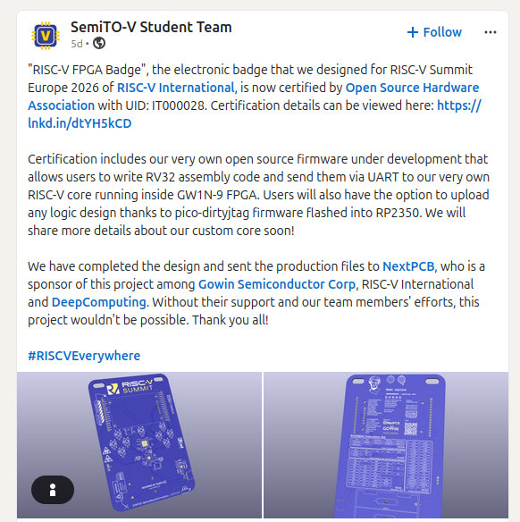 Bildquelle: https://www.linkedin.com/posts/riscveverywhere-ugcPost-7463209307203928064-RpLg/?utm_source=share&utm_medium=member_desktop&rcm=ACoAAAExd_4B88eg3uiygKywlAVeiUfK1nTPfSk ###
> Kyocera AVX: 0201-Kondensatoren mit 10 µF. 4V Nennspannung! Naja, etwas knapp fuer 3.3V Aber okay fuer 2.5V Rails vermutlich nicht schlecht. Vanye
S B _ P E 2 W O P O E P R P I N S C # V W V V L V I [ O S [ E _ [ # # # G C P E C C ] R K ] L D ] [ [ [ N _ W G C S / 1 / / 7 A / ] ] ] G D R 4 4 4 4 4 4 4 4 4 3 3 3 8 7 6 5 4 3 2 1 0 9 8 7 AMBER[2] / SPI_MOSI
Characteristics if operated under different conditions. TYPICAL CHARACTERISTICS 30 30 ) 25 ) 25 ( ( n t 20 e 20 e u TJ= 25°C r T J 100°C C C o 15 d 15 c TJ= 100°C a l 10 r 10 o o , , T J 25°C IC 5 I 5 0 0 0.0 0.5 1.0 1.5 2.0 2.5 3.0 3.5 4.0 0.0 0.5 1.0 1.5 2.0 2.5 3.0 3.5 4.0 VCE, Collector−Emitter Voltage
VIN = 5 V, VCC = 5 V, LED FORWARD VOLTAGE = 3.5 VIN= 1 MF, AMB = 25°C UNLESS OTHERWISE SPECIFIED.) 25 1.4 ) ) A 20 ( 1.2 ( D T O E 15 H 1.0 −40°C R E U R 25°C C T E 10 E 0.8 85°C B L A A E 5 N 0.6 E 0 0.4 0 1 2 3 4 5 3.0 3.5 4.0 4.5 5.0 5.5 ENABLE
linewidth=2, label=key) lines[key] = line ax.set_ylabel(ylabel) ax.legend() ax.grid(True, alpha=0.3) # Format x‑axis as HH:MM:SS on EVERY subplot ax.xaxis.set_major_formatter(mdates.DateFormatter('%H:%M:%S')) # Show x-labels on ALL plots (not just bottom row) ax.tick_params(axis='x', labelbottom=True
was so getanwird,reißtunsereGesellschaftlang- Speicher sparen MacBook Air und dem Neo unfassbar at- sam,abersicherindenAbgrund.Weshalb Teure Speicherchips: Hallo Programmierer, traktive Angebote. Was Performance an- gibt man das Geld für die Stromspeicher helft uns!, c’t 8/2026, S. 3 geht – von Performance
Entwicklungsumgebung ST MEMS Studio unterstützt. Das Adapterboard STEVAL-MKI257A für die LSM6DSK320X und das Adapterboard STEVAL-MKI258KA für die ISM6HGK256X werden bis November 2026 im eSTore und über Distributoren verfügbar sein. Die LSM6DSK320X für Consumer-Anwendungen arbeitet über einen breiten
mit 2,5 mm x 3 mm x 0,83 mm erhältlich und für Bestellungen ab 1000 Stück ab 4,6 US$ für die verbraucherorientierte LSM6DSK320X sowie ab 5,1 US$ für die industrietaugliche ISM6HGK256X verfügbar. [/c] ### FLIR
LANG=en_US.UTF-8 zur entsprechenden Sprache, also z.B. LANG=de_DE.utf8 und speichert mit Strg+O -> Enter und Strg+X. Tastatur-Layout. Um das Tastatur-Layout auf der Konsole anzupassen, muss man die Datei /etc/vconsole.conf
Makefiles „Welcome to the C++ Cache!“ - eine Einführung in C++ Fortsetzung von „Scratch“ aus Ausgabe 1, 3, 4, 5 und 6 Fortsetzung von „the python pit“ aus Ausgabe 1, 2, 3, 4, 5 und 6 Ausgabe 8. Die Ausgabe 8 vom Dezember 2012 behandelt folgende Themen: „Skutter Returns“ - Fortsetzung von „Skutter“ aus Ausgabe
g L ] P b si t A 8 6 e r S T 1 . a p E [ , ] D s 0 u 0. b [ a 1 0 0 6 b 0 0 . 0 . 0 t i [ 0 [ ] 0 [ h n 5 3 2 5 2 a oi 0 ° . . 8 . f u – 0 0 [ l tr ° o p e 0 8 5 f d e u n 0 0 o o ] G P i m 0 l m . 2 7 c u [ A 0 0 e x D 2 C W 0 0 X y a 4 0 2 E 1 o M 2 ] 4 I 0 8 b y - 7 0 V . . t o P 0 0 M 0 0 a b [ 0 O 3 E p ti O . . T i I e l S 9 0 O e V t p B D D o h n 7 2 N e f I 1 1 X E m o 0 0 2 f 4 r m 4 R 9 x o 1 9 A ] 1 t o . 3 2 2 5 –
Electronic Systems G11 / 48 Apr. 2024, Revision 20 a member of the Christ Company Group Document No.: E461201 Touch-it XELO Operating Instructions 2.3 Interfaces Connector Side (CPU T56N) 2 x USB Host (Type A) USB 4 x USB Host (Type A) (optional) Ethernet 2 x 1 GB Ethernet Communication 1 x RS-232 Video
, 3.3MHz 0.9 x VDD - - V V OL Low Logic Output Level IOUT = 100uA, 3.3MHz - - 0.1 x VDD V V IH High Logic Input Level - 0.8 x VDD - - V V IL Low Logic Input Level - - - 0.2 x VDD V ICC, SLEEP ICC,Sleep mode
, 3.3MHz 0.9 x VDD - - V V OL Low Logic Output Level IOUT = 100uA, 3.3MHz - - 0.1 x VDD V V IH High Logic Input Level - 0.8 x VDD - - V V IL Low Logic Input Level - - - 0.2 x VDD V ICC, SLEEP ICC,Sleep mode
Spezifikationen und Verfügbarkeit vermeldet man Folgendes: [c] Chorus 2 clock generators deliver up to 2x better performance, 2x lower jitter and up to 2.5x less output skew and greater spread spectrum clock support . . . Chorus 2 replaces up to 8 or 12 discrete oscillators or clock signals with a single
generator. Product is in volume production. Samples available immediately: SiT95272 (12 outputs at 6 mm x 6 mm 48 pin quad flat no-lead, QFN, package), SiT95278 (8 outputs at 5 mm x 5 mm 40 pin QFN package). [/c] ### Microchip DSA504RT- strahlungsgehärteter Taktgenerator mit sechs Ausgängen Im
ppcl dai u T 2 - T 5 .......................1 0 1 4 2 6 mm Achse I Schraube M 3 x 6 miii F 7 r I p R 24 100 kIl 4 Schrauhen M 3 x 16 111111 I) I - D 8 ........... L L I), rot, 501111 R 77 I MI) 5 Muttern M 3 1)91)11) 1)19 D21) DII) 1N4001 R14 2201 4 Schrauben M 4 x 55 rnmi D II
1 - e(-t / RC)) DD 2. With V IH= 0.3 x VDD , the time 1 at which VIHis reached satisfies to V(t1) = 0.3 x DD = VDD x (1 – e(1t / PU b )) leading to t = 0.3566749 x R x C 1 PU b 3. With V OH = 0.7 x VDD , the
lancierte mit dem SNA5000X-E ein ähnliches Produkt, das außerdem vergleichsweise preiswert ausfällt. Preisinformationen zur 3 und zur 6GHz-Variante finden sich in den Bildern, unter der URL https://youtu.be/ViAM2waWocI gibt es
einen mechanisch robusteren “Gap Filler”.  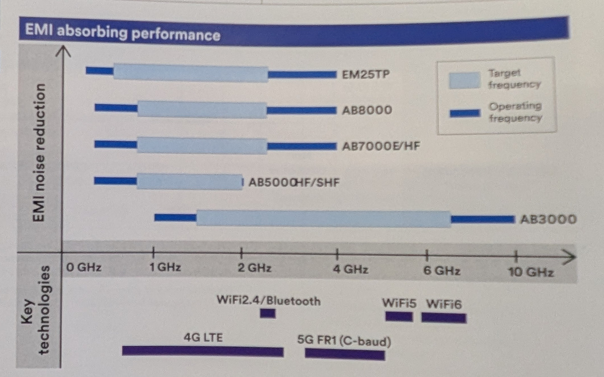  Allgemein hat 3M keine Angst vor innovativen Aufbauten – das 3D-gedruckte Demoboard für die leitfähigen Klebebänder verdient ebenfalls eine lobende Erwähnung
i f “B” “B” “B” O “F” “F” “F” a M “E” “E” Solder pot 7 “A” Closed “E” “A” Th.023oles “A” .038 x .150 3 end (0,58) (0,97 x 3,81) 0 Dia. min. Inside Dia. x Deep 8 (not a thru hole) 4 , Figure1 Figure2 Figure3 A , c i n “D” “D” r “D” F “C”
E E l l l l IL I L 4 3 2 1 e e e e NN N N 4 3 2 1 EE E E M M M M // / / C C C C A 86 8 6 J J J 4 3 2 1 c U 1 1 9 8 h X 1 0 n A l / J E C J I I 5 T 1 O L e C 2 U H 1 N N - E - N R 2 H R E E ) E ) O 8 N
FYO 010 INH PPIJLSE 012 Cl—I 01 013 vcOOuT Cl —2 5 FYI 014 RXI 014100 C1 1 1MHz RX2 CD4060 S T 1 ( X ) - ZENER Rege isp, ref f ST2 II 1C3 12 9 01 I 02 RESET,: : 0 0 n 03 Pt V 04 ST3 05 5T7 +5V bis +15V 06 f out 07 C5 + c C 7 1 c 08 09 010 SIB OCn lOOn 011 k e r jk e r Ik e r 012 Bud 2: Schaltbild der
MPU/MCU MC68HC908JB8(SOP28) ADP-68HC908JB8-S28 No Need WA68908 V5.43 FREESCALE MPU/MCU MC68HC908JK1E ADP-68HC908JK3 No Need WA68908 V5.43 FREESCALE MPU/MCU MC68HC908JK1E(SOP20) ADP-68HC908JK3-S No Need WA68908 V5.43 FREESCALE
continuous junction SD3112 4.7 0.246 0.80 3.1x3.1x1.2 o temperature rating for the MCP1640/B/C/D is +125 C. SD3114 4.7 0.251 1.14 3.1x3.1x1.4 To quickly estimate the internal power dissipation for SD3118 4.7 0.162 1.31 3.8x3.8x1.2 the switching
Ferrite beads/120200mAMHz GND 3 7 R7 1KRST VDDA 3.3V Analog voltage 5V 4 8 3.3V MCU1A C23 C24 CON4-X2 10uF 0.1uF PA0 34 PA0 PE0 141 PE0 PA1 35 142 PE1 MCU1B GND R8 1. The purpose of the 1K resistor here is to provide current limiting
e b c 2 1 1 | 1 I a L M s i e 8 s B e d t Z m n o e n t e f - - t Cd >>s b CÖu -Hx Xi Wt *ü J t/1 ,H rH C •H o c M XI h i> $) *—' [0 U >> <H üP O) W ca •a N ryj r-H HD XI T3 -P od 0 r-l O oO X) W EI 15
E y ∂E ρ system designers face just such a challenge from ∇⋅ E = x + + z = the uncontrolled release of electrical charge into ∂x ∂ y ∂z ε their designs. The most familiar example of For the case of two
AND CLOCK CHAIN 8 x 8 BiPORT SRAM ARRAY 32,768 Hz CRYSTAL A0-A12 POWER DQ0-DQ7 8184 x 8 SRAM ARRAY LITHIUM CELL E1 VOLTAGE SENSE E2 AND V PFD SWITCHING W CIRCUITRY G VCC VSS AI01377C Doc ID 2412 Rev 8 7/33 Operation modes
