-
 Bild
Bild
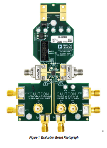
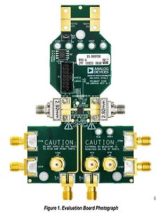
Evaluation Board von Analog Devices
J12 05-080938 REV-A 297 C0053 0068 ANALOG DEVICES AHEAD OF WHAT'S POSSIBLE RF-SERIAL CYCLER PRIMARY SIDE RFOUT 2.92mm 2.92mm CAUTION: DO NOT APPLY DC VOLTAGES TO RF IN AND RF OUT PORTS. CAUTION: EXTERNAL DC BLOCKING IS REQUIRED ON THE RF PORTS. IFIN IFRN IFRP STNC VCM GND1
-
Thread
Mazda 6 GG/GY (AUX mit Spannungsversorgung)
einem MOSFET bemuehen und komme genau hier nicht weiter. Laut Googles Gemini soll ich eine "high side" Schaltung in Betracht ziehen, habe aber da noch nichts gefunden was ich 'mal eben schnell' aufbauen kann. Mir fehlt auch die MOSFET Bezeichnung und was ich noch beachten muss. Edit: das Line-In
ist ein NPN-Darlington Die bringen dir alle drei nicht so viel, weil sie wegen NMOS/NPN eher Low-Side-Schalter sind. Und statt dem BC547 aus meinem Schaltungsvorschlag alle hart überdimensioniert. Am ehesten noch der IRFZ44, braucht dann aber einen Gatedriver mit Chargepump. Wird vom Bauteile-Aufwand
-
Thread
Raspberry 4 mit Infineon Profet und BSS123
Schaltung aufgebaut (siehe Anhang): Raspberry PI GPIO -> Standard MosFET BSS123 -> Infineon High Side Switch 6133D Mit einer Mini-Last (1k) kann ich den Ausgang zw. (fast) 0V und 12V hin- und herschalten => OK. Mit dem Display als Last bricht die GPIO Spannung ein (von 3.2 auf ca. 2.8V). Das Display
Nik N. schrieb im Beitrag #7835920: > Raspberry PI GPIO -> Standard MosFET BSS123 -> Infineon High Side Switch > 6133D Warum nimmst Du nicht einfach etwas wie den BTS462T? Kannst Du direkt mit 3.3V ansteuern.
-
 Bild
Bild
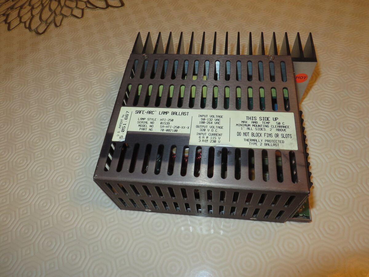
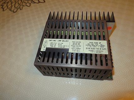
Safe-Arc Lamp Ballast
INPUT VOLTAGE 98-132 VAC 180-264 VAC OUTPUT VOLTAGE 520 V INPUT CURRENT 6 A @ 132 V 3 A @ 230 V THIS SIDE UP MAX TEMP 50 °C MINIMUM MOUNTING CLEARANCE 1" ALL SIDES 2" ABOVE DO NOT BLOCK FINS OR SLOTS THERMALLY PROTECTED TYPE 2 BALLAST PATENT NO 5 051 667
-
 Bild
Bild
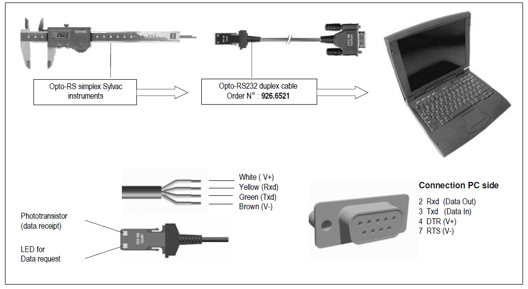
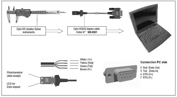
Verdrahtungsschema Opto-RS232 Kabel zu PC
Yellow (Rxd) Green (Txd) Brown (V-) Phototransistor (data receipt) LED for Data request Connection PC side 2 Rxd (Data Out) 3 Txd (Data In) 4 DTR (V+) 7 RTS (V-)
-
Thread
ARM-AI-Assistent final, RP2040 mit 200 MHz Maximaltakt uvm
sich nun die Vorstellung folgender neuer Features: [c] Much less RAM is used when loading maps side by side Better address searching Asynchronous map loading [/c] ### Android 16 – Beta mit Channel Sounding-Support verfügbar Im Hause Google gibt es ebenfalls Neuerungen: Android 16 ist in
-
Thread
Auerswald DLC 4830 Lichtcomputer
wird beides sicher auch für die Tasten/LED Matrix genutzt...inkl- drei Transistoren für die High-Side der LED Matrix Und eine Analogecke um das Musiksignal zu nutzen... Prozessor ist speziell gelabelt im DIP28 Gehäuse...
-
 Bild
Bild
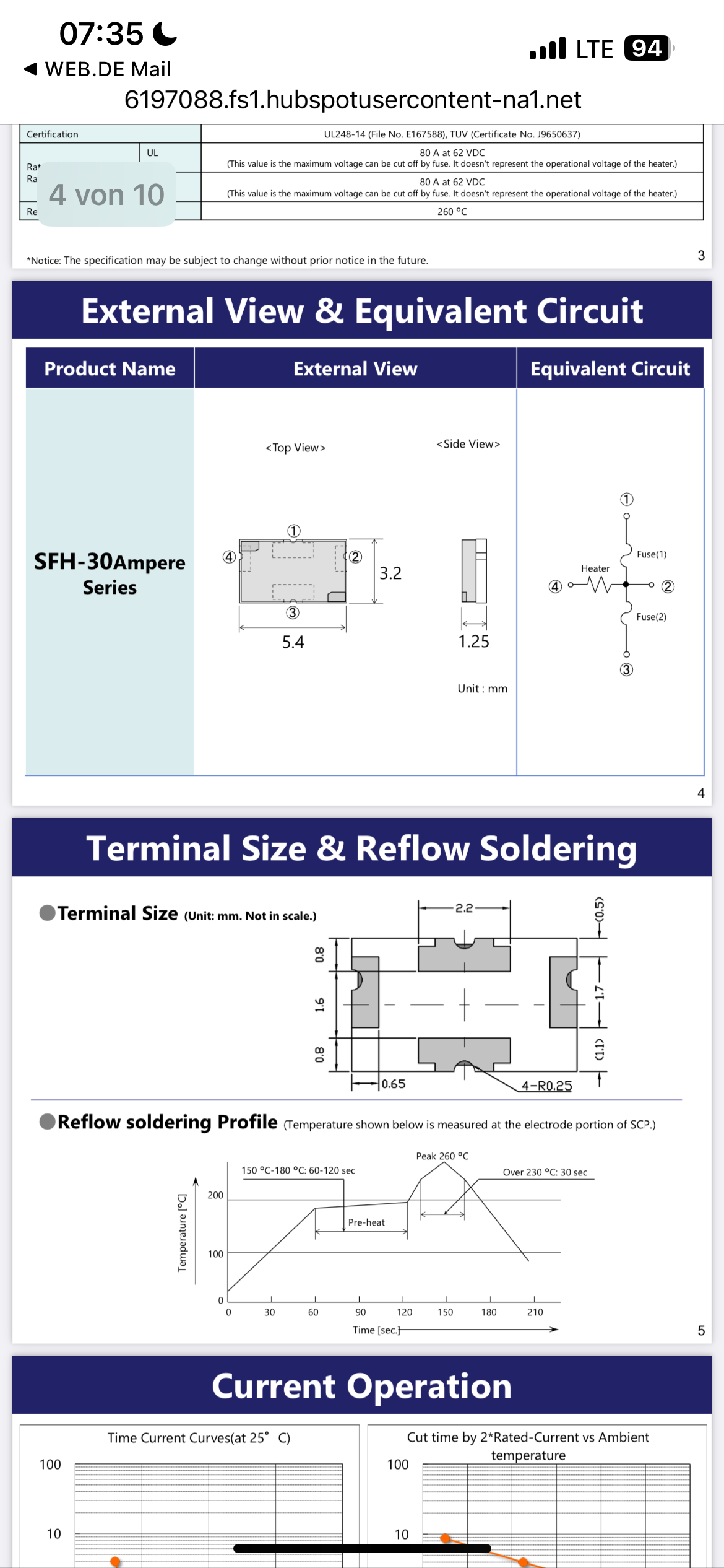
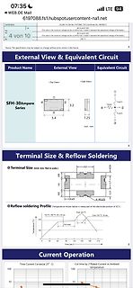
Datenblatt Ausschnitt SFH-30Ampere Series
prior notice in the future. External View & Equivalent Circuit Product Name External View <Top View> <Side View> Equivalent Circuit 1 4 2 3 SFH-30Ampere Series Heater 1 4 2 3 5.4 1.25 Unit: mm Terminal Size & Reflow Soldering Terminal Size (Unit: mm. Not in scale.) 0.8 1.6 0.65 2.2 1.7 4-R0.25 0.8 Reflow
-
Thread
OpAmp symmetische Versorgung oder negative Hifsspannung ?
d.h. bei einem Rail-to-Rail muss die Hilfsspannung größer als der maximale Spannungsabfall am Low-Side Transistor sein. Lothar M. schrieb im Beitrag #7832800: > Übliche R2R OP schaffen das locker, wenn sie beim "auf-Null-ziehen" von > einem Pulldown am Ausgang unterstützt werden. Das ohmsche
Betracht zu lassen. Solange die negative Versorgung größer als der maximale Spannungsabfall am Low-Side Teil der Ausgangsstufe (inkl. eines ggf. vorhandenen Pull-Downs) ist, beeinflußt die Restspannung die Ausgangsspannung (im Rahmen der Regelgenauigkeit) nicht. > ... oder noch schlimmer: da könnten
-
Thread
LEDs mit gemeinsamen GND schalten
#7832696: > Grundsätzlich bin ich für alles offen. Ach, ist das so? Und was hast du bisher über "HighSide-Switches" herausbekommen?
damit umgehen und LEDs in so einer WS2811-Treiberkette die Adressen passend zuweisen kann. Den High-Side Treiber bräuchte man trotzdem zusätzlich.
-
 Bild
Bild
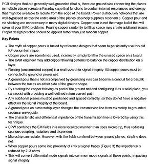
Text über PCB Design und Copper Pours
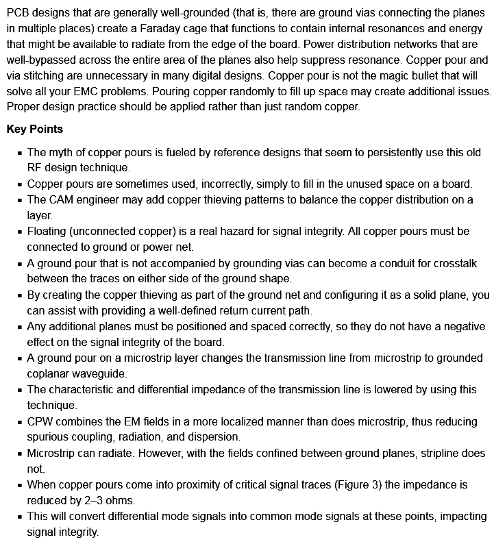
not accompanied by grounding vias can become a conduit for crosstalk between the traces on either side of the ground shape. ■ By creating the copper thieving as part of the ground net and configuring it as a solid plane, you can assist with providing a well-defined return current path. ■ Any additional
-
 Bild
Bild
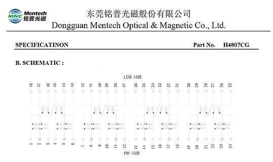
Schaltplan eines Transformators
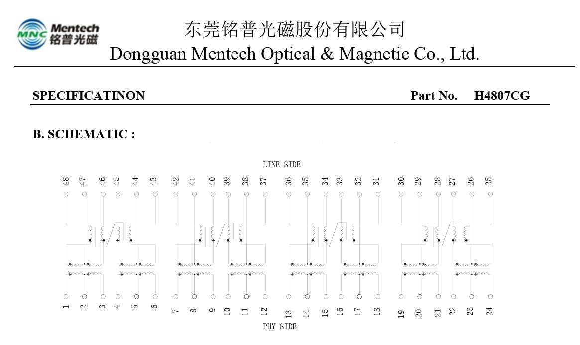
Dongguan Mentech Optical & Magnetic Co., Ltd. SPECIFICATINON Part No. H4807CG B. SCHEMATIC : LINE SIDE 48 47 46 45 44 43 42 41 40 39 38 37 36 35 34 33 32 31 30 29 28 27 26 25 1 2 3 4 5 6 7 8 9 10 11 12 13 14 15 16 17 18 19 20 21 22 23 24 PHY SIDE
-
Artikel
Konstantstromquelle
beschriebene LM317 eignet sich besonders gut als Stromquelle, da er seine Regelspannung auf der 'high-side' erwartet (1,25 V zwischen Vout und ADJ) und man den Regelpfad als Konstantstrompfad missbrauchen kann (ADJ als Ausgang nach GND, wobei der Strom über den Widerstand und nicht von ADJ geliefert wird
solid #ccccff" Neben diesen Einschränkungen ist auch zu beachten, dass Die Last R 1 auf der High-Side hängt und nicht gegen GND. Praxisbeipspiel: Der LDO-Regler "AP7331-WG-7" arbeitet mit einer niedrigen Referenzspannung von nur 0,4V und die Dropout-Spannung beträgt bei 140mA auch nur 0,2V. Also muß
-
Thread
PDF-Dateibrowser gesucht
www.kas-bmu.de/publikationen.html https://www.csb.gov/ http://www.eisenbahn-unfalluntersuchung.de/cln_032/sid_A8C3F590F4C5DE5CF0C2A88B57DEAEF1/EUB/DE/Home/homepage__node.html?__nnn=true https://www.bsu-bund.de/DE/Publikationen/Unfallberichte/Unfallberichte_node.html https://www.gov.uk/government/organisations
-
Thread
Schneller 8bit Treiber gesucht
Unterschied zwischen Tri-State-Ausgang und Open-Drain-Ausgang sein, wenn man von ersterem nur den Low-Side-Treiber benutzt? Open-Kollektor musst du wahrscheinlich schon ziemlich suchen. > Beim 74F299 habe ich das im ersten Datenblatt noch nicht gesehen. Der besitzt genau ein gemeinsames Output Enable
-
 Bild
Bild
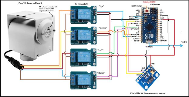
Verdrahtungsplan Arduino Micro mit Relaismodulen und Beschleunigungssensor
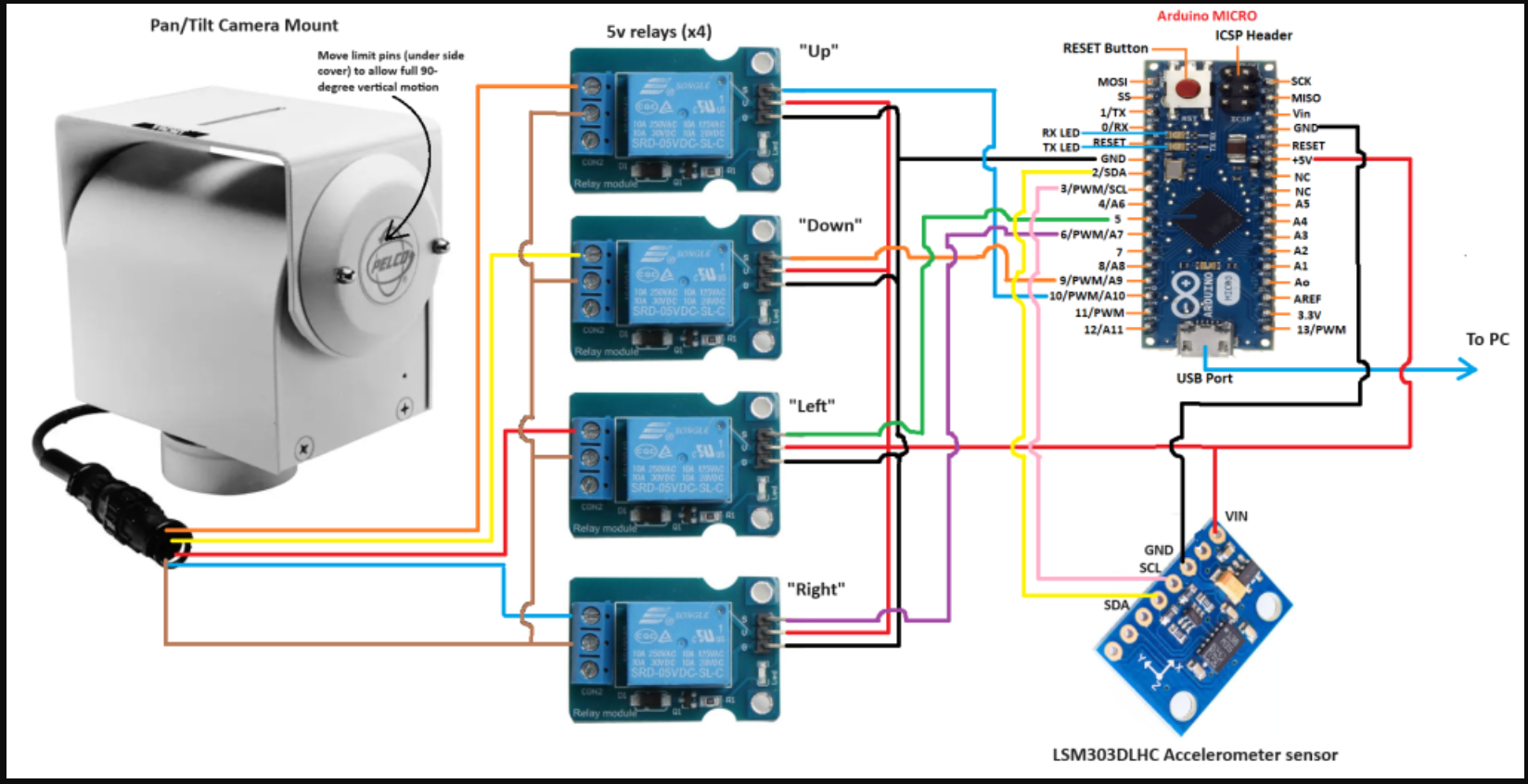
Pan/Tilt Camera Mount Move limit pins (under side cover) to allow full 90-degree vertical motion 5v relays (x4) "Up" "Down" "Left" "Right" Arduino MICRO RESET Button ICSP Header MOSI SCK 1/TX MISO RX LED GND RESET GND TX LED +5V GND A5 2/D2 A4 3/D3
-
 Bild
Bild
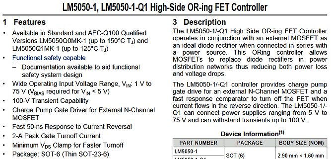
Datenblatt Ausschnitt LM5050-1 High-Side OR-ing FET Controller
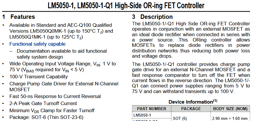
LM5050-1, LM5050-1-Q1 High-Side OR-ing FET Controller 1 Features LM5050Q0MK-1, LM5050Q1MK-1 VIN: 1 V to 75 V 100-V Transient Capability N-Channel MOSFET 3 Description LM5050-1/-Q1 Device Information PART NUMBER: LM5050-1, PACKAGE:
-
Thread
3 LEDs an 2 Leitungen
mit einem NPN habe ich mal dazu. Wobei, wenn der TO einen Signalturm verwendet, müsste man 'High-Side' Switching machen, da hier eine gemeinsame Masse ist. Das ist aber auch nicht das Problem. Funktionieren tut mein Teil.
Thomas S. schrieb im Beitrag #7825302: > müsste > man 'High-Side' Switching machen, da hier eine gemeinsame Masse ist. Das > ist aber auch nicht das Problem. Doch genau das war mein ursprüngliches Problem! Für die vielen Ideen die zusammengekommen sind, danke
-
 Bild
Bild
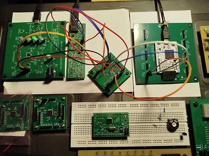
Elektronik-Aufbau mit mehreren Leiterplatten und Breadboard
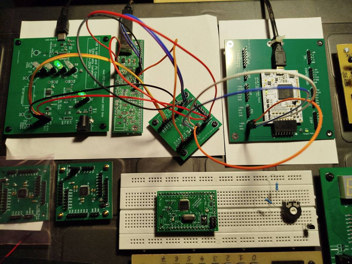
USB, PC Connector, Client (ISO) side, Target (ISP) side, ICSP, 36 kHz
-
 Bild
Bild
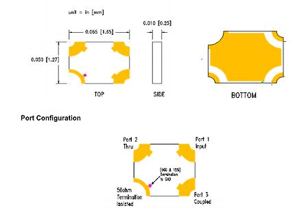
PCB-Dimensionen und Port-Konfiguration
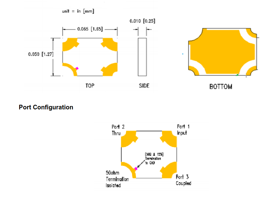
unit = in [mm] 0.065 [1.65] 0.010 [0.25] 0.050 [1.27] TOP SIDE BOTTOM Port Configuration Port 2 Thru Port 1 Input [500 ± 15%] Termination to GND 50ohm Termination Isolated Port 3 Coupled
-
Thread
Suche Protection IC
Vllt passt dir ja einer https://www.infineon.com/cms/de/product/power/smart-power-switches/high-side-switches/profet-industrial-smart-high-side-switch/
probieren ob der Ausgangsstrom wieder unterm Limit bleibt? Constant-Current? ...? Soll das Ding High-Side oder Low-Side eingesetzt werden? Wenn High-Side - bist Du Dir ganz sicher dass es High-Side sein muss und es nicht auch Low-Side ginge?
-
Thread
avrdude.conf, wo finde ich die Argumente?
mit archiviert. Was man auf jeden Fall dann noch auf dem Zielsystem benötigt ist ein Qt5 mit PySide2 oder Qt6 mit PySide6. Das können und dürfen wir natürlich nicht mit ausliefern, aus lizenzrechtlichen Gründen.
immer ohne ausgekommen und war eigentlich nur Neugierig. > Wie oben geschrieben, du musst Qt + PySide (von Qt gelieferte > Python-Integration) vorher installieren. Ja, das genau hindert mich daran weiter Neugierig zu sein.
-
Thread
Interpolation nicht äquidistanter Messdaten
Verstaerker "highside" messen, oder das Ganze > potentialfrei machen. Also der Shunt ist low side und der wird vorverstärkt es geht sich hier um die Messung der Spannung. Diese wird über einen Spannungsteiler gemessen der eben 250 Teilungsfaktor hat.
-
Thread
Win10 zerschossen, Lubuntu von USB-Stick drauf, perfekt!
what-debian-version-are-the-different-ubuntu-versions-based-on 24.04 LTS Noble Numbat trixie/sid debian 13 LTE bis 2027, ergo aktuell
-
Thread
Magnetisch betätigen Schalter für Tauchlampe
eingebautem Schutz? - muss ja nicht wieder brennen. https://www.mouser.at/new/onsemi/onsemi-low-side-smart-discrete-fet/ Sg
-
Thread
Einstellbare Konstantstromquelle - Welcher OP Amp?
Musst du unbedingt High-Side regeln? Low-Side würde ein LM358 völlig reichen.
H. H. schrieb im Beitrag #7812745: > Musst du unbedingt High-Side regeln? > > Low-Side würde ein LM358 völlig reichen. High Side oder Low Side ist völli egal weil man ja auch den komplementären Transistor hat. Ob Rail to Rail notwendig hängt nur davon ab,
-
Thread
Neues Mainboard
VmWare-Player). Geholfen hat mir dieser Tipp: https://forums.linuxmint.com/viewtopic.php?p=2382121&sid=cfd523b5df56e2253fbfc4c3860b91cb#p2382121 - Shut down your virtual machine, and quit VMware Workstation Player. - Open your virtual machine ".vmx" file with a text editor, find "virtualHW.version
-
Thread
u-blox steigt aus IoT-Funkmodulgeschäft aus, Container für Echtzeitbetriebssystem, RP2350 von Olimex
security architecture, we’ve been working to develop an implementation of AES which is hardened against side-channel attacks (notably differential power analysis), and we’ll be challenging you to defeat it. Check back next week for more details. [/c] Interessant ist außerdem ein kleiner Seitenhieb gegen