. Das ist mir aber auch egal... Gut, den Strom habe ich nicht beobachtet aber bei 10.5V sind es ca 200mA die benötigt werden laut Labornetzteil... Eigentlich ist mir nur wichtig das ich eine stabile 10.5V Stromversorgung habe für eine lange Zeit. Kein schnickschnack, keine Spielerei. Stabil und langlebig
Messing. Warum nicht https://www.amazon.de/Proxxon-27110-Micro-Fr%C3%A4se-MF-70/dp/B002H5AH5O/ref=asc_df_B002H5AH5O/ oder https://www.sieg-machines.de/Fraesmaschine-SX1 ?
Positionierung des Querschlittens. Technische Daten 230 V 100 W 50/60 Hz 5.000 - 20.000/min. Tisch 200 x 70 mm Verfahrwege: X (quer) 134 mm, Y (längs) 46 mm, Z (hoch) 80 mm Maschinenfuß (Aufstellfläche) 130 x 225 mm Gesamthöhe 370 mm Gewicht ca. 7 kg Artikelnummer: 27 110 mal sehen vllt. ist
OUT ISINK Output Sink Current VOUT = 3V 50 mA VOH High Level Output Voltage IO= –10µA 2.995 V IO= –200µA ● 2.7 2.99 V V Low Level Output Voltage I = 10µA 0.005 V OL O IO= 1.6mA ● 0.09 0.4 V OV DD= 2.5V VOH High Level Output Voltage IO= –200µA 2.49 V VOL Low Level Output Voltage IO= 1.6mA 0.09 V OV DD
Exposure to Absolute Maximum Rating condi- tions for extended periods may affect device reliability. Refer also to the STMicroelectronics SURE Program and other relevant qual- ity documents. 2. Minimum DC voltage on Input or Output is –0.5V with possible undershoot to –2.0V for a period less than 20ns.
CCond= 5pF, Min Typ Max Unlts SLHT Differential Swing Low-to-High Transition TimR RLOADA== 270 ohm 170 200 230 n ps EXTCLOAD= 5pF, o SHLT Differential Swing High-to-Low Transition TimREXT_SWING 270 ohm 170 200 e230 ps u s l I2S Audio AC Specifications (under normal operating conditions unless otherwise specifiad
des genauen Produktes achten: 220V und die Station inkl. kolben einstellen, klappt nicht dies als Ref. im Link zu übergeben. Und darauf achten ob VS Kostenlos oder mit Betrag der zum Preis dazukommt) https://de.aliexpress.com/item/1005005820847973.html https://de.aliexpress.com/item/1005004446393897
Deine Einschätzung Carsten, die verlinkte Aixun T3A könnte mir schon gefallen. 2sek Aufheizen mit 200W klingt nach genug Reserve für (Ent-)Lötungen, wo mein LR20 auch schon mal mit breitester Spitze an seine Grenze gekommen ist (IGBTs und Leistungs-LED mit großflächigen Lötpads). Das wäre dann schon
specified Symbol Parameter Conditions Min Typ Max Units tTLH THL Output Transition Time V DDe 5V 100 200 ns V DDe 10V 50 100 ns V DDe 15V 40 80 ns tPLH PHL Propagation Delay Time Trigger Operation— A or B to Q or Q V DDe 5V 300 600 ns V DDe 10V 150 300 ns V e 15V 100 220 ns DD Reset Operation— C Dto Q
----------------- 2990 '------- Graphische Darstellung --------- 3000 CLS :SCREEN 2 3010 WINDOW (0,200)-(200,0) 3020 VIEW (400,0)-(639,189) 3030 LINE (0,0)-(200,200),,B 3040 FOR N=1 TO 9 3050 LINE (N*20,0)-(N*20,200),,,&H2222 3060 LINE (0,N*20)-(200,N*20),,,&H2222 3070 NEXT N 72 Quarzfilter, eine kleine
without interface option. If you need a longer cable, please consult with our sales staff. For details, refer to CO/USB series datasheet. Master unit cancontrol multipleunits connectedas sla(Thefunctionis not allowedtooutput theaveragecurrent fromeachpower supply connectedinparallel.) Master/slave (A) (A)
Flash memory (PIC16F1847/PIC16LF1847) : 11 = Write protection off 10 = 000h to 1FFh write-protected, 200h to 1FFFh may be modified by EECON control 01 = 000h to FFFh write-protected, 1000h to 1FFFh may be modified by EECON control 00 = 000h to 1FFFh write-protected, no addresses may be modified by EECON
https://www.amazon.de/dp/B09PPV58K4?psc=1&ref=ppx_yo2ov_dt_b_product_details ...passen 1:1... Tantal-Elko bei Reichelt.
wieder der Hobbytheoretiker, eine Menge Ahnung von nichts. Ich habe hier zwei NiMH-Blöcke, Tronic 200mAh (Lidl) und TopCraft 250mAh (Aldi). Über Nacht 11,5h mit 25mA geladen und dann mal gemessen: Bei ungefähr 15mA Last bricht der Tronic von 10 auf 8,8 Volt ein, also Ri ungefähr 80 Ohm. Das Fluke77
genaueren bereits digitalisierten Wert zu bekommen. Die Steuerregister des ADC. ADMUX. Referenzspannung: REFS1, REFS0 REFS1 REFS0 Referenz 0 0 externe Referenz 0 1 interne Referenz: Avcc 1 0 wird beim Mega8 nicht benutzt 1 1 interne Referenz: 2,56 Volt Ausrichtung: ADLAR ADLAR Auswirkung 0 Das Ergebnis wird
0 1 0 4 0 1 1 8 1 0 0 16 1 0 1 32 1 1 0 64 1 1 1 128 Beispiel: 8 MHz Prozessortakt: 8.000.000 Hz / 200.000 Hz = 40 Da mit 200 kHz gerechnet wurde (maximale Frequenz), nimmt man den nächsthöheren Wert, also 64. 8.000.000 Hz / 64 = 125.000 Hz = 125 kHz So erhält man bei 8 MHz einen Prescaler von 64 und
try not to modify this register, just modify the mic_sens_gain register, see the text for details Refer to the "Setting Modulation Limits and MIC Sensitivity" section of the file. (2) TONE1, TONE2 generation Register Address(HEX) Description Enable TONE1 tone1_gen REG_70H[15] tone1_gain[6:0] REG_70H[
LM2776 CMOS charge-pump voltage converter inverts a positive voltage in the range from 2.7 V to • 200-mA Output Current 5.5 V to the corresponding negative voltage. The • Inverts Input Supply Voltage LM2776 uses three low-cost capacitors to provide • Low-Current PFM Mode Operation 200 mA of output current
[ Ta=85℃ V 1400 d 1400 e 1200 : 1200 a g l 1000 l 1000 V 800 o 800 u t p 600 o 600 r 400 o 400 D D 200 200 0 0 0 50 100 150 200 0 50 100 150 200 Output Current: OUT[mA] Output Current:OUT[mA] XC6902NC01 CIN 1.0μF(ceramiL), C = 1.0μF(ceramic) 2000 Ta=-40℃ ] 1800 m 1600 Ta=25℃ i Ta=85℃ d 1400 : 1200 g
noch viel mehr von der Platine, wenn die nicht 100% sauber ist. Der MUX hat zwar im Signalpfad 200MHz Bandbreite, kann aber nicht so schnell umschalten. Ein Diagramm geht bis 10MHz; wenn man die Schaltzeiten zusammenzählt wären evt. 40MHz drin. Das reicht natürlich für 110 oder 300 Hz, verfälscht
Wert legen müssen -- das Rauschen taucht als ungewollte Phasenmodulation seines GPSDO auf... Die Ref ADR441 ist in diesem Frequenzbereich wohl nicht spezifiziert, konnte kein Rauschspektrum im Datanblatt finden) -- und rauscht auf jeden Fall schon mit 1.2uVpp oberhalb von 0.1Hz. Ich würde mir doch
OFF pin tied to V INC IN = 1.0 µF, and C OUT = 4.7 µF (unless otherwise noted) 250 1mA 10mA 50mA ) 200 V m t 150 u o p 100 r D 50 0 -75 -50 -25 0 25 50 75 100 125 150 Temperature (°C) Figure 6-7. Dropout Voltage vs Temperature for Legacy Chip Figure 6-8. Dropout Voltage vs Temperature for New Chip 200
samples normiert (wie im ersten Beispiel der Dokumentation) https://de.mathworks.com/help/signal/ref/goertzel.html#mw_497d20c5-6e25-4c3a-9dd7-a4b61b8dd383 Als Eingangssignal dient ein zusammengesetztes Sinussignal aus drei Sinuswellen mit den den Frequenzen 100,200 und 300 Hz, die Amplitude beträgt
einlaufen im Vergleich zu den untersuchten Die zu untersuchenden Frequenzen sind im Vektor f = [100,200,300] enthalten, das ist schon korrekt. Das zusammengesetzte Sinussignal besitzt die Frequenzen 100, 200 und 300Hz, es sei denn, der Buffer, der vorgeschaltet ist verändert aus irgendeinem Grund die
: 105 ℃ 1000 h ● Vibration-proof product (30G guaranteed) is available upon request (ø8 ≦) ● AEC-Q200 compliant ● RoHS compliant Specifications Category temp. range –40 ℃ to +105 ℃ Rated voltage range 6.3 V to 100 V Capacitance range 1 μF to 1500 μF Capacitance tolerance ±20 % (120 Hz / +20℃) Leakage
SET UP TIME 500ms/230VAC, 1200ms/115VAC 100 ~ 305VAC 142VDC ~ 431VDC VOLTAGE RANGE Note.5 (Please refer to "STATIC CHARACTERISTIC" and “ DRIVING METHODS OF LED MODULE"section) FREQUENCY RANGE 47 ~ 63Hz POWER FACTOR (Typ.) PF≧0.97 / 115VAC, PF≧0.95 / 230VAC, PF≧0.92 / 277VACat full load (Please refer
high-side source sense pin voltage (SHx) –5 (2) VVDRAIN+ 5 V Transient 200-ns high-side source sense pin voltage (SHx) –10 V VDRAIN+ 10 V Continuous low-side gate drive pin voltage (GLx) –1.0 V + 0.3 V VGLS Transient 200-ns low-side gate drive pin voltage (GLx) –5.0 VVGLS+
SPECIFICATION 12.1 ELECTRICAL CHARACTERISTICS Ta = 25°C ITEM CONDITION SPEC. UNIT LINEARITY 1.5 % X AXIS 200 ~ 900 TERMINAL RESISTANCE Y AXIS 200 ~ 900 Ω INSULATION RESISTANCE DC25V 20 MΩ INPUT VOLTAGE 5(TYP.) V 12.2 PRECAUTIONS IN USE OF TOUCH PANEL 12.2.1 PURPOSE: IN ORDER TO PREVENT ACCIDENTAL USE AND
): 110 x 120 x 135 mm 150 °C)genutzt,können die anderen beiden Temperaturspei- Abmessungen Kolben: 200 x 30 mm cherplätze für verschiedene Lötaufgaben, wie z. B. das Löten BAU- UND BEDIENUNGSANLEITUNG 4 BAU-UNDBEDIENUNGSANLEITUNG auf der Leiterplatte oder das Verlöten von Abschirmgehäu- Bild1:Haupt-
): 110 x 120 x 135 mm 150 °C)genutzt,können die anderen beiden Temperaturspei- Abmessungen Kolben: 200 x 30 mm cherplätze für verschiedene Lötaufgaben, wie z. B. das Löten BAU- UND BEDIENUNGSANLEITUNG 4 BAU-UNDBEDIENUNGSANLEITUNG auf der Leiterplatte oder das Verlöten von Abschirmgehäu- Bild1:Haupt-
C to +70°C −25°C to +70°C Maximum Operating Voltage 5.5 VDC, 3.5 VDC, 6.5 VDC 5.5 VDC Capacitance Refer to Table 1 Refer to Table 1 Refer to “Measurement Conditions” Capacitance Allowance +80%, −20% +80%, −20% Refer to “Measurement Conditions” Measured at 1 kHz, 10 mA; See also ESR Refer to Table 1 Refer
Tolerance (5%), K Tolerance (10%), M Tolerance (20%) Rated Voltage Range 6 – 125 V DF (120 Hz at 25°C) Refer to Part Number Electrical Specification Table Leakage Current Refer to Part Number Electrical Specification Table (t rated voltage up to +85°C and 2/3 of rated voltage applied at 125°C) Approved failure
Hz Sine Wave) VDRM = 90 V MKP3V120 VDRM = 180 V MKP3V240 ON CHARACTERISTICS Breakover VoltageBOI= 200 mA V BO V MKP3V120 MKP3V240 110 - 130 220 - 250 Breakover Current BO - - 200 mA Peak On-State Voltage V TM - 1.1 1.5 V (TM = 1 A Peak, Pulse Width ≤ 300 ms, Duty Cycle ≤ 2%) Dynamic Holding Current
500 nA Output Short-Circuit Sink I OUT asserted, OUT = V 10 mA SC CC MAX6460 Reference Short-Circuit REF = GND 7 mA Current TA= -40°C to +85°C 2.183 2.25 2.303 Reference Output Voltage V REF V TA= +85°C to +125°C 2.171 2.25 2.303 Sourcing: 0 ≤ I ≤ 100µA, Load Regulation REF 50 µV/µA sinking: 0 REFI ≤ 300nA
Impedanz von real 8 Ohm. Nominell wird der Chinese wahrscheinlich rechnen 200*200/4 -> 10kW. Da solche Module mit 100W angeprisen werden, wirst du nur um die 5W sauber rausbekommen.
sie die Power und den Bereich nicht > [...] > Nominell wird der Chinese wahrscheinlich rechnen 200*200/4 -> 10kW. In Rätseln du sprichst. > Da solche Module mit 100W angeprisen werden, wirst du nur um die 5W > sauber rausbekommen. Quatsch. Rainer hat ja sogar die passende Abbildung (THD_vs_Outputpower
Panel for SDS1072CML
Siglent Stop
ΔT=84.00µs
1/ΔT=11.90kHz
CurB=80.00µs
CurA=-4.00µs
<10Hz
CH1 -- 200mV
M 10.0µs
M Pos:0.00µs
CH1 \ 224mV
Menu On/Off
Intensity Adjust
Cursors Acquire
Save/Recall
Default Setup
Single
Measure Display Utility Help
Run/Stop
Vertical V<->mV
Horizontal V<->mV s<->ns
Auto
Trigger Trig Menu
Set to 50%
CH1 CH2
Ref
Position
Zoom Hori Menu
Force Level
Print
G(tot) Table 5 gives the typical and maximum values for gate charge parametersG(tot)QGS and QGD ; refer to Fig. 7 for definitions of these parameters. Table 5. BUK7S1R0-40H data sheet characteristics: gate charge Symbol Parameter Conditions Min Typ Max Unit QG(tot) total gate charge ID= 25 A; VDS = 32
AEAT-6010-A06 10 -40 to +125 Serial +5.0 Notes: 1. For other options of Magnetic Encoder, please refer to factory. Table1. AbsoluteMaximumRatings [2,3] Parameter Symbol Limits Units Notes DC SupplyVoltage at pinV DD = 5V VDD -0.3 to + 7 V InputVoltage Vi -0.3 toVDD+0.3 V StorageTemperature TSTG -40
OPERATE AT CREATER THAN 132 VAC WITH 400 Hz AC LINE)
LINE 150 VA MAX
FUSE 3A 230V
SELECT 115V 120V 200V 240V
NOM FREQ 400 Hz 60 Hz
MAX 1.4A 0.80A
CAUTION: VOLTAGE FOR SERVICEABLE PARTS INSURE INSTRUMENT REFERRING TO QUALIFIED PERSONNEL
HP-IB
METRIC! THIS INSTRUMENT USES ENGLISH HARDWARE CONSULT MANUAL
CAUTION: REFER TO SERVICE MANUAL BEFORE REMOVING ANY COVER
HEWLETT-PACKARD USA
SER 2948A03658
OPT 001
10 MHz
EXT REF IN 5V PK MAX
REF OUT
DIGITAL PORT
OUTPUTS
HIGH 1
LOW
HIGH 2
LOW
WARNING: FOR CONTINUOUS PROTECTION
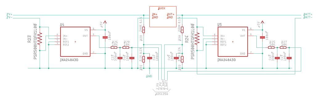
Available Gains: >> – INA240A1: 20 V/V >> – INA240A2: 50 V/V >> – INA240A3: 100 V/V >> – INA240A4: 200 V/V > > Gain = Verstärkung Was Gain heisst, weiss ich. nur die Benennung mit 20V/V... bedeutet es der 20V/V hat eine 20fache Verstärkung, der 200V/V eine 200fache?
beschaffen. ich denke ich werde beim INA240 bleiben mit externen Shunts. Noch ne Frage bezüglich der REF eingänge: Habe ich es richtig verstanden, daß wenn REF1 auf GND und REF2 auf VCC verbunden sind, daß sich dann eine Ausgangsspannung von VCC/2 bei 0A einstellt? (bidirectionaler Betrieb) und das wenn
by Knight (ref 2), who wound 22 coils on an Amidon FT 50-61 ferrite core (diameter of 12.7 mm) with from 4 to 36 turns. A comparison of his measurements and the equation developed here for that core is plotted below
to permit the neglect of losses, the parallel resonance formula reduces to: 2 1 (2πf )0= L(C +C ) L ref Where C isLthe self-capacitance, and C refis the added parallel capacitance including all strays. Rearranging gives: C =−C + 1 ref L (2πf ) L2 (1.1) 0 which, insofar as the lumped component representation
Circuit Figure 20 VOUT Output Voltage 7V ≤ V IN≤ 40V, 0.2A ≤ ILOAD ≤ 3A 5.0 V 4.800/4.750 V(min) 5.200/5.250 V(max) η Efficiency V IN= 12V, ILOAD = 3A 80 % (1) Typical numbers are at 25°C and represent the most likely norm. (2) All limits specified at room temperature (standard type face) and at temperature
scale of the main time base. Parameter Name Type Range Default Value <scale_value> Discrete Please refer to Explanation ---- Explanation:Default to set the main time base. time base gear: {5.0ns|10.0ns|20.0ns|50.0ns|100ns|200ns|500ns|1.0us|2.0us|5.0us|10us|20us|50us| 100us|200us|500us|1.0ms|2.0ms|5.0ms
Short Current Protection Voltage VCC=3.6V VSIP¡VOI2¡^ 1.00 1.35 1.70 V Overcharge Delay Time TOC 80 200 ms Overdischarge Delay Time VCC=3.6V to 2.0V TOD 40 100 ms Overcurrent Delay Time (1) VCC=3.6V TOI1 10 20 ms £gs Overcurrent Delay Time (2) VCC=3.6V TOI2 500 Charger Detection Threshold Voltage VCHA
multiplication : 3 cycles • Interrupts (save PC/PS) : 6 cycles (16 priority levels) (Continued) Be sure to refer to the “Check Sheet” for the latest cautions on development. “Check Sheet” is seen at the following support page URL : http://www.fujitsu.com/global/services/microelectronics/product/micom/support/

 Bild
Bild
 Bild
Bild
 Bild
Bild