-
PDF
mic23050.pdf
cycle. Power loss is equal to the 0.47µH inductor may be used. For lower output ripple, a high sid2 MOSFET R DSON multiplied by the Switch 2.2µH is recommended. Current . During the off cycle, the low side N-channel MOSFET conducts, also dissipating power. Device Maximum current ratings of the inductor
in „LDO und Step-Down-Converter parallel“ · Analoge Elektronik und Schaltungstechnik ·
-
PDF
slyt584_SEPIC_2xDr_Step-Up-Down_Buck-Boost.pdf
metal-oxide semiconductor field-effect converter are three popular non-inverting buck-boost transistor (MOSFET), a diode, and an inductor. When the topologies. The Zeta converter, also called inverse SEPIC, MOSFET (Q1) is ON, the voltage across the inductor (L1) is similar to SEPIC, but less attractive than
in „Weidezaun gegen Schnecken mit Netztrafo und Rohr DN160 für Hobbygärtner“ · Projekte & Code ·
-
PDF
slua110.pdf
are required to insure proper operation of the PWM while delivering the high current drive pulses. MOSFET Input Impedance Typical gate-to-source input characteristics of most FETs reveal approximately 1500 picofarads of capacitance in series with 15 nanohenries of source inductance. For this example, the
in „Boost Konverter“ · Mikrocontroller und Digitale Elektronik ·
-
PDF
DW01A-DS-10_EN.pdf
0.100 150±30 l y ’ s n 6. Pin Configuration and Package Marking Information i e O Pi1 No. SODbol MOSFET gate connection pin for discharge control e 3 OCS MOSFET gate connection pin for charge control c 6 5 A 5 VCC Power supply, through a resistor (R1) n DW01 6 GND Ground pin r o r e 1 2 3 . . P . A f
in „LiFePo Balancer: CF-4S30A-A“ · Analoge Elektronik und Schaltungstechnik ·
-
PDF
DW01A-DS-10_EN.pdf
0.100 150±30 l y ’ s n 6. Pin Configuration and Package Marking Information i e O Pi1 No. SODbol MOSFET gate connection pin for discharge control e 3 OCS MOSFET gate connection pin for charge control c 6 5 A 5 VCC Power supply, through a resistor (R1) n DW01 6 GND Ground pin r o r e 1 2 3 . . P . A f
in „Laderegler Li-Ion 3s“ · Analoge Elektronik und Schaltungstechnik ·
-
PDF
canbusboard.pdf
1 2 3 4 5 6 Power Mosfets Endstops Driver A A File: power.kicad_sch File: mosfets.kicad_sch File: endstops.kicad_sch File: driver.kicad_sch Communication Controller Thermistor B B File: communication.kicad_sch File: controller.kicad_sch
-
PDF
BTN7970_DS_11.pdf
-7-11 drive applications. It is part of the NovalithIC™ family containing one p-channel highside MOSFET and one n-channel lowside MOSFET with an integrated driver IC in one package. Due to the p-channel highside switch the need for a charge pump is eliminated thus minimizing EMI. Interfacing to a microcontroller
in „Wärmeableitung Motortreiber BTN7970B (PG-TO263-7-1)“ · Mikrocontroller und Digitale Elektronik ·
-
PDF
BTN7970.pdf
-7-11 drive applications. It is part of the NovalithIC™ family containing one p-channel highside MOSFET and one n-channel lowside MOSFET with an integrated driver IC in one package. Due to the p-channel highside switch the need for a charge pump is eliminated thus minimizing EMI. Interfacing to a microcontroller
in „Halbbrücke BTN7970 Motorstromüberwachung“ · Mikrocontroller und Digitale Elektronik ·
-
PDF
l7987.pdf
necessary to drive the internal power switch. The high-side driver for embedded N-channel Power MOSFET switch and bootstrap circuitry. A dedicated high resistance low-side MOSFET, for anti-boot discharge management purposes, is also present. The peak current limit sensing block, with programmable
in „L7987, wie Output regeln?“ · Analoge Elektronik und Schaltungstechnik ·
-
PDF
2013821185244121.pdf
Plastic-Encapsulate Mosfets Dual N-Channel Enhancement Mode MOSFET FEATURES 8205A 5A,20V.r DS(on)0.025 @ VGS= 4.5 V rDS(on) 0.040 @ VGS = 2.5 V. TSSOP-8 Absolute Maximum Ratings (TA=25oC, unless otherwise noted) P aram eter
in „Laderegler Li-Ion 3s“ · Analoge Elektronik und Schaltungstechnik ·
-
PDF
AN1543-D.PDF
B to achieve stable and reliable operation. Of course, this can 500 easily be done by using two MOSFET devices, but the cost 400 increases significantly, keeping the ON losses constant, compared to the BIPOLAR transistors. However, for low 300 0 200 400 power/low line voltage applications, the MOSFET
in „Reparatur EVG für T5 Röhre“ · Analoge Elektronik und Schaltungstechnik ·
-
PDF
VMM1500-0075P.pdf
Dual Power VMM 1500-0075P V DSS = 75 V ID25 = 1500 A MOSFET Module R DS(on) = 0.55 m Ω Phaseleg Configuration Preliminary data 3 8 9 1 11 10 2 MOSFET T1 + T2 Features Trench MOSFETs Symbol Conditions Maximum Ratings – low R DSon – optimized intrinsic reverse
in „Impulsströme“ · Analoge Elektronik und Schaltungstechnik ·
-
PDF
Linear_Current_Sense_AN105.pdf
supply. In single-supply operation (V at ground), theoutput rangemaybeoffset Adding two external Mosfets to hold off the voltage al- EE lows the LTC6101 to connect to very high potentials and upwards by applying a positive reference level to V BIAS monitor the current flow. The output current from the
in „'High Side' Strom Messen - Geht das so ?“ · Analoge Elektronik und Schaltungstechnik ·
-
PDF
AN105.pdf
supply. In single-supply operation (V at ground), theoutput rangemaybeoffset Adding two external Mosfets to hold off the voltage al- EE lows the LTC6101 to connect to very high potentials and upwards by applying a positive reference level to V BIAS monitor the current flow. The output current from the
in „High-Side Strommessung AVR (Shunt)“ · Mikrocontroller und Digitale Elektronik ·
-
PDF
IC_Brochure.pdf
Power MOSFETs External*) External*) StallGuardM - YES Package SO28 SO28 *)over4Awithadditionalpre-drivers: TheTMC239andTMC249arecombinedwitheightexternalLow-RDS-ONhighefficiencyMOSFETs forcurrentsofupto4Aandvoltagesofupto28.5VDC.Withadditionalexternalpre-drivers
in „Schrittmotor Ansteuern - Lösungen“ · Mikrocontroller und Digitale Elektronik ·
-
PDF
FS14KM-9.PDF
MITSUBISHI Nch POWER MOSFET FS14KM-9 HIGH-SPEED SWITCHING USE FS14KM-9 OUTLINE DRAWING Dimensions in mm 10 ± 0.3 2.8 ± 0.2 3 . 0 ± 3 ± . 0 3 6 ± φ 3.2 ± 0.2 1 . . ± 0 . 1.1 ± 0.2 4 3 1.1 ± 0.2 1 0.75 ± 0.15 0.75 ± 0.15 2.54 ±
in „High speed switching mosfet“ · Analoge Elektronik und Schaltungstechnik ·
-
PDF
EB_104.pdf
threshold voltages. Since output of four devices without the added loss and cost of the power gain of a MOSFET is largely dependent on the power splitters and combiners. Motorola MRF150 RF power drain bias current, only m matching is required, and it can relatively high power levels. This technique is considered
in „Stackpole Ferrit Kerne für RF Verstärker“ · HF, Funk und Felder ·
-
PDF
irfh5300pbf.pdf
IRFH5300PbF ® HEXFET Power MOSFET V 30 V DS R DS(on) max 1.4 m: (@V GS= 10V) Q g (typical) 50 nC R G (typical) 1.3 : ID (@T = 25°C) 100 h A PQFN 5X6 mm c(Bottom) Applications • OR-ing MOSFET for 12V (typical) Bus in-Rush Current • Battery Operated DC Motor Inverter MOSFET Features and Benefits Features Benefits Low R DSon (≤ 1.4mΩ) Lower Conduction Losses Low Thermal Resistance to PCB (≤ 0.5°C/W) Enable better thermal dissipation 100% Rg tested Increased Reliability
in „Beschaltung Mosfet für Brushless-Regler“ · Analoge Elektronik und Schaltungstechnik ·
-
PDF
JW1501ABr0.4_C371169.pdf
Notice DESCRIPTION FEATURES JW1501A/B is a high performance Primary Side ● Integrated with 650V MOSFET Regulation (PSR) power switch with high ● Multi Mode PSR Control precision CV/CC control ideal for charger ● Audio Noise Free Operation for PSR applications. ● Optimized Dynamic Response for PSR ●
in „SNT Gartenbeleuchtung defekt, pulst aber“ · Analoge Elektronik und Schaltungstechnik ·
-
PDF
AN-1358.pdf
through the main internal circuit breaker multiple windings wound on a single gapped core. For sim- MOSFET exceeds 390mA. If current limit is triggered, the plification, we refer to the first, driven winding, as the primary switching regulator is automatically disabled by discharging and the main output
in „PoE: wie runterregeln ?“ · Mikrocontroller und Digitale Elektronik ·
-
PDF
Cell_balancing_TI_Application_Note.pdf
charge transfer. PowerPump uses an n- and The bq78PL114 features three selectable balancing p-channel MOSFET pair and a power inductor to complete algorithms: a charge-transfer circuit between an adjacent pair of cells. • Terminal-voltage pumping is just like the voltage- Shown in Figure 5, the MOSFETs and
in „LiFePo4 Balancer/Überwachungsschaltung im Auto“ · Mikrocontroller und Digitale Elektronik ·
-
PDF
datasheet_HIP_4081A.pdf
power MOSFET. 14 ALS A Low-side Source connection. Connect to source of A Low-side power MOSFET. 15 VCC Positive supply to gate drivers. Must be same potentDDl(Pin 16). Connect to anodes of two bootstrap diodes
in „HIP 4081 Verständnisprobleme“ · Mikrocontroller und Digitale Elektronik ·
-
PDF
Dr.Arbeit_H-Bruecken.1455549.pdf
the MOSFET’s pin resistances R , R D anG R . The Sarameters used for the considered power MOSFET are listed in Table 6.1. The circuit operates in three different cases. In the first state, assuming a smaller gate
in „DIY 10kW/20kWh eta=99% Insel ESS Projektvorstellung“ · Haus & Smart Home ·
-
PDF
viper100-e.pdf
PWM circuit together with an optimized, high ■ INTERNALLY TRIMMED ZENER voltage, Vertical Power MOSFET (620V/ 3A). REFERENCE Typical applications cover offline power supplies with a secondary power capability of 50W in wide ■ UNDERVOLTAGE LOCK-OUT WITH HYSTERESIS range condition and 100W in single range
in „Hochvoltspannungsregler“ · Analoge Elektronik und Schaltungstechnik ·
-
PDF
VIPer100.pdf
PWM circuit together with an optimized, high ■ INTERNALLY TRIMMED ZENER voltage, Vertical Power MOSFET (620V/ 3A). REFERENCE Typical applications cover offline power supplies with a secondary power capability of 50W in wide ■ UNDERVOLTAGE LOCK-OUT WITH HYSTERESIS range condition and 100W in single range
in „VIPer50 Flyback Schaltnetzteil“ · Analoge Elektronik und Schaltungstechnik ·
-
PDF
MAX1758.pdf
. Connect SHDN to VL for normal operation. 18 PGND Power Ground. Current from the low-side power MOSFET switch source flows through PGND. 19, 20 LX Power Inductor Switching Node and High-Side Power MOSFET Source 21 CS Battery Current-Sense Positive Input. Connects to internal 0.1Ω resistor between BATT
in „Verständnisfrage Strom für MAX1758“ · Mikrocontroller und Digitale Elektronik ·
-
PDF
bruecke.pdf
0V AUSL 3 Hyst Vcc 5 1nF 2 3 °C 100n 1GND 2 TLP290 VOS628A GND C5 MCP9501 60deg 1.0nF 60V 2mOhm-Mosfet 1.5nF 60V 1mOhm-Mosfet D1,D2: RF05VYM2SFHTR(200V,11ns,SOD323) oder DO-214AC 2.0nF 80V 1mOhm-Mosfet R4 B6T41_RF05VYM_ES1D O R5 6 BAT41_RF05VYM_ES1D O POS 1 R15 10µD1 . NEG 1 R17 10µ D2 . 68 C1 5 5 68
in „PV Simulator für Batteriebetrieb von Hoymiles & Co“ · Mikrocontroller und Digitale Elektronik ·
-
PDF
CM7N65F.pdf
R mæW3^▯fv[üu5[Pg PQlSł ▯C ▯M ▯7 ▯N ▯6 ▯ ▯w▯w▯w▯▯j▯d▯s▯e▯ShenZhen Jingdao Electronic POWER MOSFET %650V N-ChannVDMOS▯ %O u(S˚ .[Xeö ▯ 2 Yu5 %{&TR▯HS {IsflOÝc▯Nä lB ▯1 ÿ; u( ▯▯ N; u(N QEu5Vh0▯▯L ▯E▯D qR¤0▯u5n ▯ MVh▯ {IT▯|{R s _▯Qsu5 ï▯ ▯2 ÿ▯N; ▯ ryp„ l _▯Qs ▯^ƒ_º 1 l ▯‘▯u5 ;\▯ÿ▯ Qeu5[„\▯ 2 ▯3 ÿ▯\
in „Schaltnetzteil aus LED Deckenleuchte“ · Analoge Elektronik und Schaltungstechnik ·
-
Bild
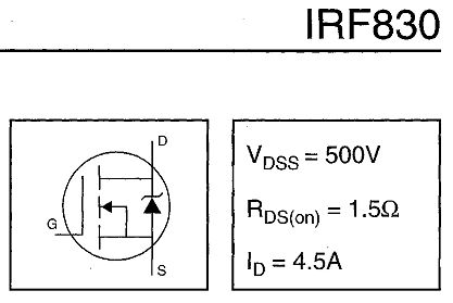
Datenblatt-Ausschnitt IRF830 MOSFET
IRF830 V_DSS = 500V R_DS(on) = 1.5Ω I_D = 4.5A G D S
in „Probleme mit Spannungsunterschieden beim Schalten“ · Analoge Elektronik und Schaltungstechnik · · Screenshots
-
Bild
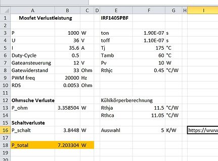
Excel-Tabelle zur Berechnung der Mosfet-Verlustleistung
Mosfet Verlustleistung IRF1405PBF P 1000 W ton 1.90E-07 s U 36 V toff 1.10E-07 s I 35.6 A Tj 175 °C Duty-Cycle 0.5 Tamb 60 °C Gateansteuerung 12 V Pv 10 W Gatewiderstand 33 Ohm Rthjc 0.45 °C/W PWM freq 20000
in „IRF1405PBF Mosfet wird zu heiss und verabschiedet sich“ · Analoge Elektronik und Schaltungstechnik · · Screenshots
-
Bild
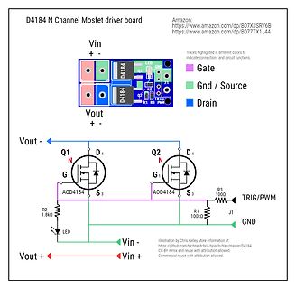
PCB-Layout und Schaltplan eines MOSFET-Treiberboards
D4184 N Channel Mosfet driver board Amazon: https://www.amazon.com/dp/B07XJSRY6B https://www.amazon.com/dp/B07TX1J44 Vin + - LED GND Q1 D4184 R2 Q2 D4184 R3 TRIG/PWM Vout + - Vout - Q1 N G1 D4 D4 AOD4184 S3 Q2 N G1 D4 AOD4184
in „12V an TIP131 mit BC548 schalten“ · Analoge Elektronik und Schaltungstechnik · · Schaltpläne
-
Bild
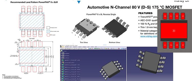
Datenblatt eines Automotive N-Channel MOSFETs
Automotive N-Channel 80 V (D-S) 175 °C MOSFET PowerPAK® 8 x 8L Reverse Single FEATURES TrenchFET® power AEC-Q101 qualif 100 % Rds(on) Thin 1.9 mm height Material categori for definitions of www.vishay.com TOP VIEW Bottom View
in „SQJQ184ER-T1_GE3 Footprint“ · Analoge Elektronik und Schaltungstechnik · · Screenshots
-
Bild
Schaltplan einer Spannungsregelung mit MOSFET und Zener-Dioden
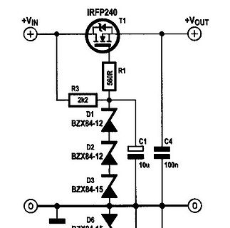
+VIN T1 IRFP240 +VOUT R1 560R R3 2k2 D1 BZX84-12 D2 BZX84-12 C1 10u C4 100n D3 BZX84-15 D6 BZX84-15
in „Brückengleichrichter mit Elko - Spannungsbegrenzung“ · Analoge Elektronik und Schaltungstechnik · · Schaltpläne
-
Bild
Schaltplan eines P-Kanal-MOSFETs mit Last
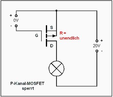
+ 0V - S R = unendlich G D + 20V - P-Kanal-MOSFET sperrt
in „Astabiler Multivibrator mit TLC555 (LMC555)“ · Analoge Elektronik und Schaltungstechnik · · Schaltpläne
-
Bild
Schaltplan einer MOSFET-Schaltung mit Zener-Dioden
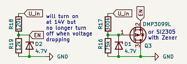
U_in will turn on at 14V but no longer turn off when voltage dropping R18 120k R19 12k EN D2 4.7V GND R17 300k R16 75k D1 4.7V 1 DMP3099L or SI2305 with Zener 2 Q3 3 GND
in „ESP32 hängt wenn Spannung von 0V ansteigt -> reset bis 14 V Solarspannung“ · Mikrocontroller und Digitale Elektronik · · Schaltpläne
-
Bild
Schaltplan mit NPN-Transistor, MOSFET und Diode
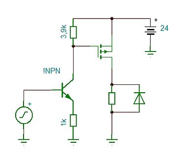
3,9k !NPN 24 1k
in „IRF4905 Ansteuerung mittels ESP32 (24V 2A)“ · Mikrocontroller und Digitale Elektronik · · Schaltpläne
-
Bild
Text und Schaltplan eines MOSFET-Audio-Verstärkers
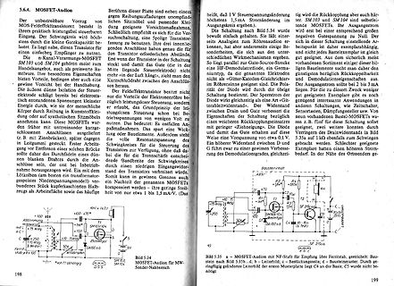
5.6.4. MOSFET-Audion Bild 5.34 MOSFET-Audion für MW-Sender-Nahbereich Bild 5.35 a KH (1 kΩ) T1 SMJ103/104 SMJ12 GA100 aa 10 kΩ 250 Ω 10 Ω 10 nF C1 C2 C3 C4 C5 10 nF 10 nF 10 nF 10 nF 10 nF 10 nF 10 nF 10 nF 10 nF
in „Gibt es diskrete Schaltungstechniken, die erst in jüngerer Zeit entwickelt wurden?“ · Offtopic · · Schaltpläne
-
Bild
Schaltplan einer Gate-Treiber-Schaltung mit MOSFETs
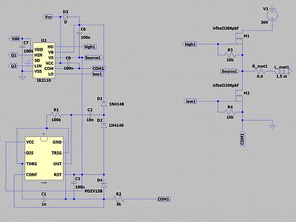
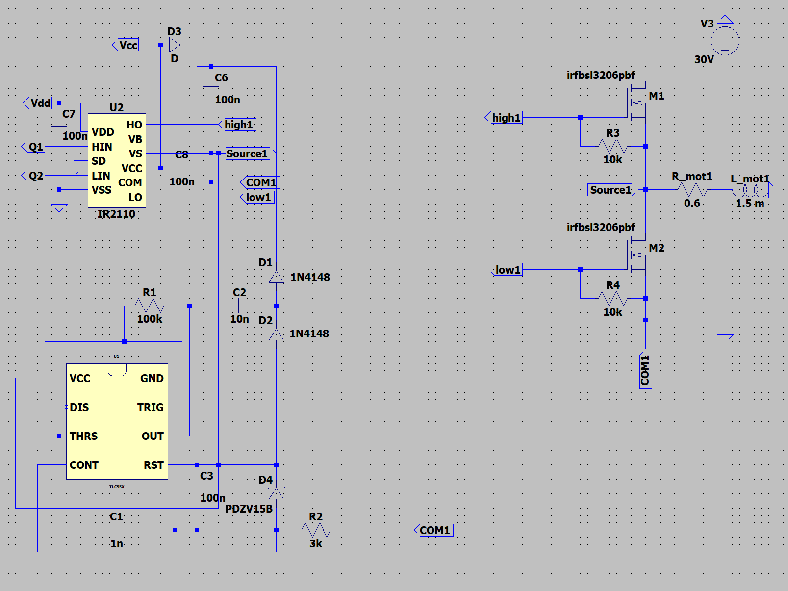
Vcc D3 V3 30V U2 HO high1 M1 Vdd C7 100n VB IR2110 R3 10k HIN SD VS Source1 C8 100n LIN COM R_mot1 0.6 L_mot1 1.5m COM1 low1 irfbsl3206pbf M2 R4 10k D1 1N4148 low1 D2 1N4148 COM1 R1 100k C2 10n U1 VCC GND DIS TRIG THRS OUT CONT RST C1 1n C3 100n D4 PDZV15B R2 3k
in „H-Brücke mit 100% Duty-Cycle“ · Analoge Elektronik und Schaltungstechnik · · Schaltpläne
-
Bild
Schaltplan einer H-Brücke mit MOSFETs und Transistoren
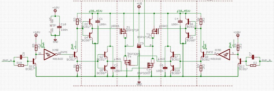
+10V, C10, 100n, IC8E, PWM1, 74106D, BC817, Q11, R10, C8, R5, 5mA, Q3, Q4, BC817, BC807, C1, 100n, HIGH1, BSP171P, T1, C3, T3, BSP3205, T4, HIGH2, C4, 100n, Q6, BC817, Q9, BC807, PWM2, IC5D, 74106D, Q8, BC817, Q7, BC807, Q10, BC807, Q12, BC817, R2, C7, PWM_B, +10V, GND, +10V, Q2, BC817, Q5, BC807, C2, 100n, LOW1, LOW2
in „Cmos H-Brücken Inverter saugt Quelle leer“ · Analoge Elektronik und Schaltungstechnik · · Schaltpläne
-
Bild
Tabelle mit Spezifikationen von P-Channel MOSFETs
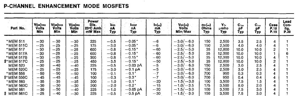
P-CHANNEL ENHANCEMENT MODE MOSFETS Part No. | V(BR)DSS Volts Min | V(BR)GSS Volts Min | V(BR)DG Volts Min | Power Dis. 25°C Amb mW Max | IDSS nA Typ | ICSSf nA Typ | ID(on) mA Typ | VGS(th) Volts Min/Max | RDS(on) Ohms Typ | Yfs uHm
in „Suche ein Datenblatt zu WM135“ · Analoge Elektronik und Schaltungstechnik · · Screenshots
-
Bild
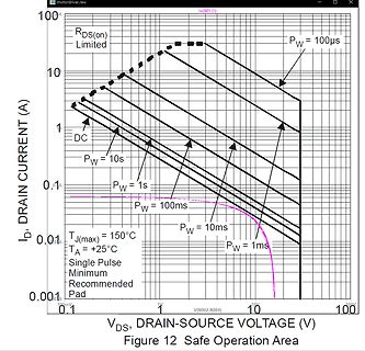
Safe Operation Area Diagramm eines MOSFETs
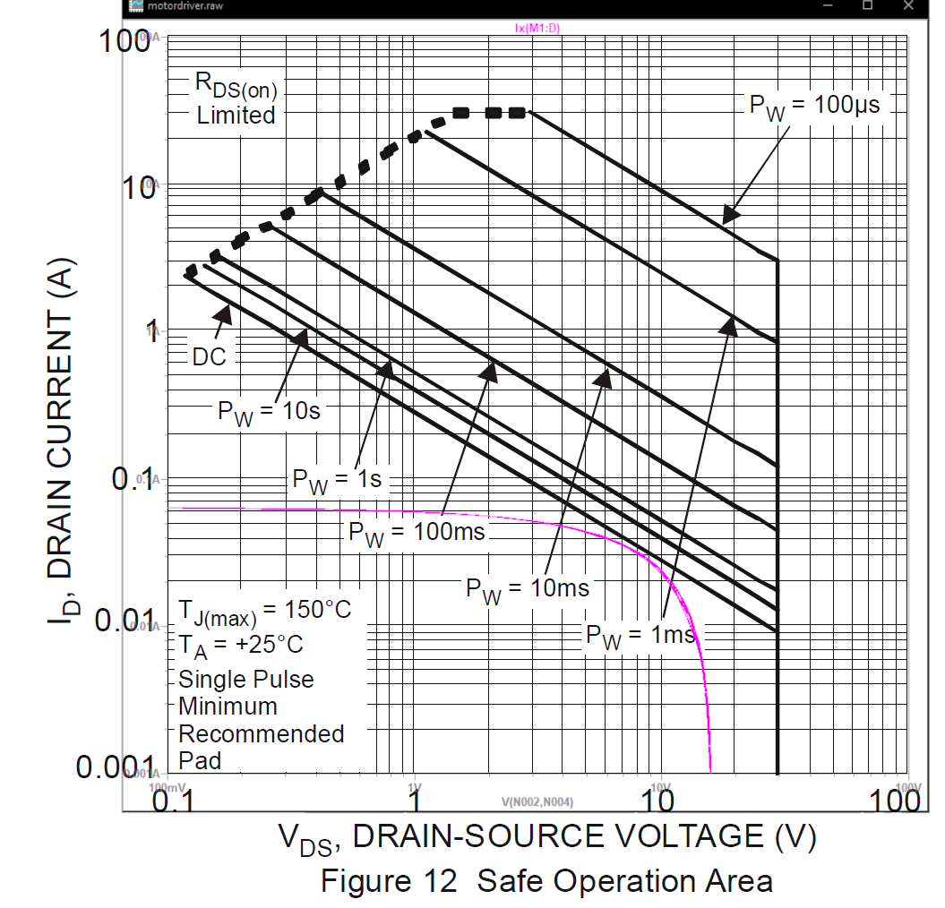
motordriver.raw 100 RDS(on) Limited 10 ID, DRAIN CURRENT (A) 1 DC PW = 100µs PW = 10s 0.1 PW = 1s PW = 100ms TJ(max) = 150°C TA = +25°C 0.01 PW = 10ms Single Pulse Minimum Recommended PW = 1ms 0.001 0.01 PAD 0.1 1V 10 100 VDs, DRAIN-SOURCE VOLTAGE (V) Figure 12 Safe Operation Area
in „Reparatur Staubsaugerroboter 360 S5“ · Analoge Elektronik und Schaltungstechnik · · Screenshots
-
Bild
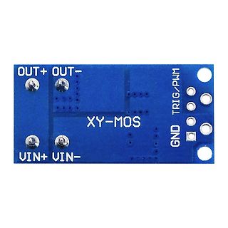
XY-MOS MOSFET Treiber Modul
OUT+ OUT- XY-MOS TRIG/PWM GND VIN+ VIN-
in „SSR DC DC 12V positiv geschaltet“ · Fahrzeugelektronik · · Platinenfotos
-
Bild
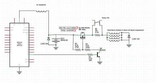
Schaltplan mit Arduino Nano, MOSFET und Relais
D4, D2, D0/RX, GND, 1,5KE 30A, 28V / 8A = ca 2 V Abfall, Temp = ca 65-80C, VCC1 28Volt DC, Q1 PNP Mosfet IRF 4905, R5 5W 4,7Ω, Step Down Module 4 stück mit Spule angedeutet, 1,5KE 12A, R3 0.25 27kΩ, R2 0.25 27kΩ, Q2 BC547C, R4 0.25 1kΩ, Relay 24v
in „P Kanal Mosfet schlägt immer wieder mal Durch.“ · Analoge Elektronik und Schaltungstechnik · · Schaltpläne
-
Bild
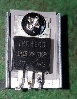
Leistungs-MOSFET IRF4905 auf Kühlkörper
IRF4905 IOR 918P 77 WS
in „P Kanal Mosfet schlägt immer wieder mal Durch.“ · Analoge Elektronik und Schaltungstechnik · · Fotos
-
Bild
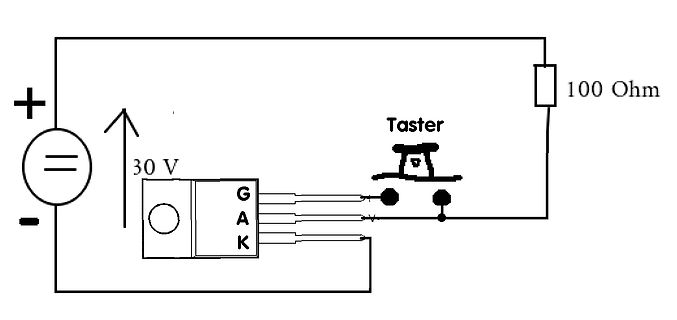
Schaltplan mit Spannungsquelle, Widerstand, Taster und MOSFET
30 V, 100 Ohm, Taster, G, A, K
in „Warum schaltet mein Thyristor nicht durch?“ · Analoge Elektronik und Schaltungstechnik · · Schaltpläne
-
Bild
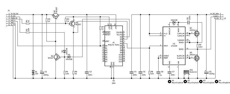
Schaltplan einer Arduino-basierten Schaltung mit MOSFETs
1 KL,20,5A 2 KL,15 3 PWM,IN 4 NTC+ 5 NTC- 6 KL,31 Q1 BC557 R3 1k R5 1k Q3 BC557 R1 1k R2 22k D2 1N4148 Q2 BC547 R4 10k R6 1k D1 15V C1 1000µ F C2 100n 28 RESET 27 RESET 18 AREF 19 A0 20 A1 21 A2 22 A3 23 A4 24 A5 25 A6 26 A7 29 GND 25 GND U1 LT158 D0/RX 1 D1/TX 0 D2 3 D3 4 D4 5 D5 6 D6 7 D7 8 D8 9 D9 10 D10 11 D11 12 D12 13 D13 14 D14 15 D15 16 D16 +5V 3V3 R7 1k VIN C4 100n C5 100n R8 10k C7 100n C8 100n 1N4148 Q4 IRFZ44N T_GATE_DR 15 T_GATE_FB 14 T_SOURCE 13 SENSE+ 12 SENSE- 11 B_GATE_DR 9 B_GATE_FB 8 Q5 IRFZ44N R9 10m HS1 Heatsink C9 1500µ F H1 MountingHole H2 MountingHole H3 MountingHole H4
in „PWM-Frequenzwandlung mit Arduino?“ · Mikrocontroller und Digitale Elektronik · · Schaltpläne
-
Bild
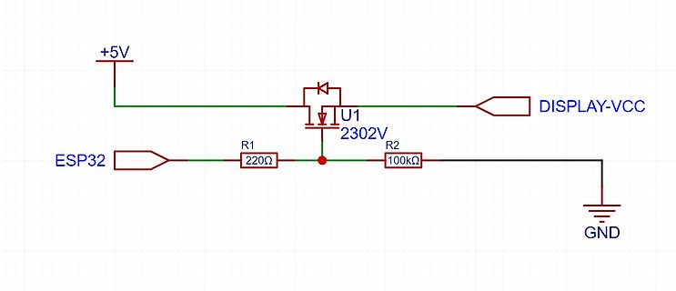
Schaltplan einer MOSFET-Schaltung zur Display-Versorgung
+5V U1 2302V DISPLAY-VCC ESP32 R1 220Ω R2 100kΩ GND
in „Probleme beim Schalten eines Displays mit MOSFET und ESP32“ · Analoge Elektronik und Schaltungstechnik · · Schaltpläne
-
Bild
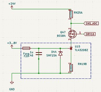
Schaltplan eines elektronischen Teils mit MOSFET und Referenzspannung
+24V RN25A 1 100k 2 SNS_ADC Q47 BSS84 1 DRV16 3 U15 TL432DBZ +3...8V Fuse F20C46 1u D44 SMF15A 2 RN19B 100k 7 GND
in „V-Ref und verstärker IC gesucht/ Komplementär-TL431“ · Analoge Elektronik und Schaltungstechnik · · Schaltpläne
-
Bild
Schaltplan mit MOSFET, LED und Reed-Schalter
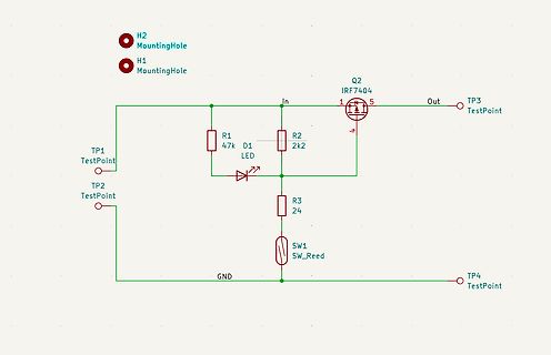
H2 MountingHole H1 MountingHole Q2 IRF7404 In 1 5 Out TP3 TestPoint R1 47k R2 2k2 D1 LED TP1 TestPoint TP2 TestPoint R3 24 SW1 SW_Reed GND TP4 TestPoint
in „Magnetisch betätigen Schalter für Tauchlampe“ · Analoge Elektronik und Schaltungstechnik · · Schaltpläne
-
Bild
Schaltplan mit PIR-Sensor, MOSFET und MCU
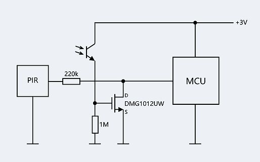
PIR 220k +3V MCU D DMG1012UW S 1M
in „PIR Bewegungssensor, der aber nur bei Dunkelheit anspricht“ · Mikrocontroller und Digitale Elektronik · · Schaltpläne