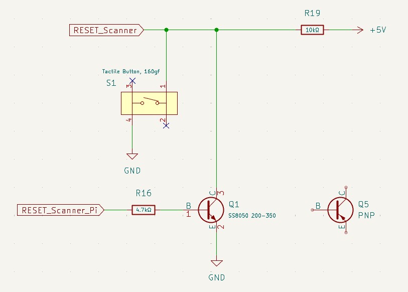
10mA deshalb habe ich diesen Wert auch Verwendet. Fazit: der BC547C könnte das locker, da sein ß als Schalttransistor mit dieser Ansteuerung gut genug ist. Eine Lichterkette mit 200 LEDs kann er aber nicht. Das Problem ist ja gelöst.
https://de.aliexpress.com/item/Transistor-Sortiment-Kit-BC337-BC327-2N2222-2N2907-2N3904-2N3906-S8050-S8550-A1015-C1815-10-wert-200/32837521623.html Langfristig, weil die Lieferzeit schon mal zwei Monate betragen kann. Alle Transistoren in dem Set sind 08/15 Typen in Bastler-Qualität. Von den Daten
VIN0.7 VCC —20 —50 —80 mA RESET Input current IR VIN0.13 VCC —3 —8 —15 mA 2 Pull-up (IN=IL) 20 50 80 mA SS Input current *6 SS Pull-down (INVIH —6 —15 —25 mA P1, P2 input current P1, P2 VINV IH —300 —600 —900 mA 2 VINV IL —10 —40 —80 mA *7 At hardware power down Ñ Ñ 10 Power Down Mode I Ta=25°C, CC=2.0 V
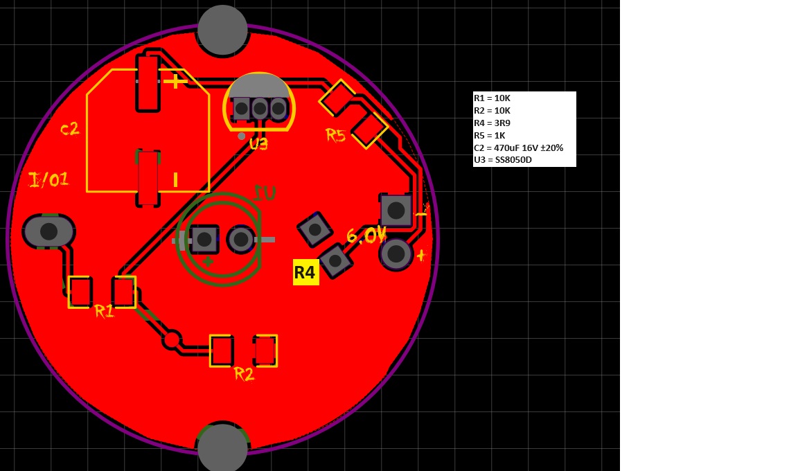
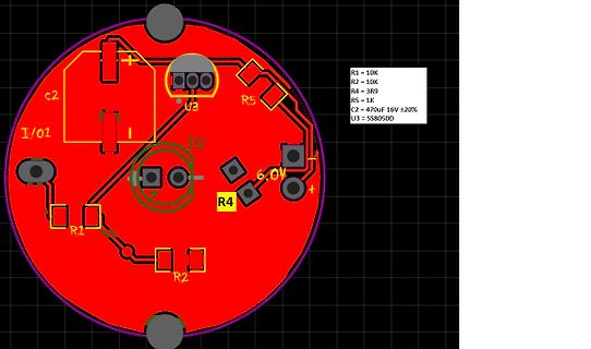
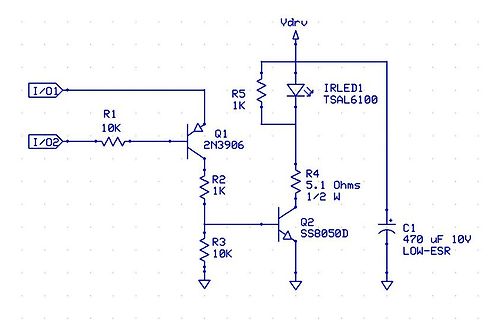
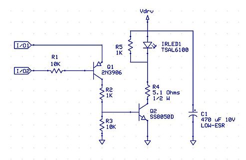
beängstigend beim Schraubenzieher-Test, würde keinen Finger-Test machen wollen... Transistor ist ein 8050SS (1.5 A). Ist in etwa die Schaltungsvariante aus dem Bigclive-Video hier: https://www.youtube.com/watch?v=vvXZM6kg_gI
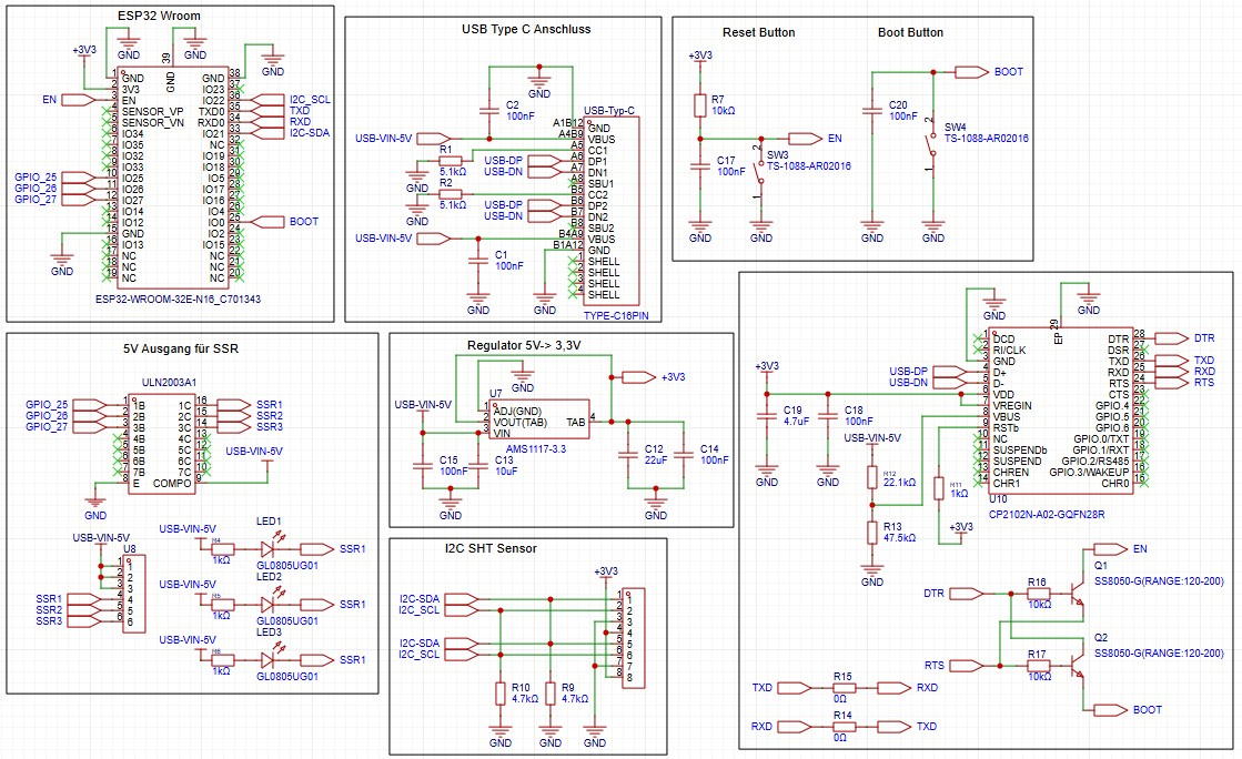
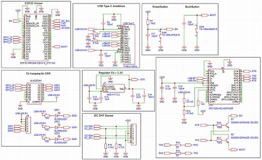
herauszufinden welche Bauteile noch defekt sein könnten. Vor den Relais gibt es noch weitere Transistoren (SS8050) und ich vermute das einer davon defekt ist. Was meint ihr? Gruss und Danke für eure Hilfe Chris
900ss D. schrieb im Beitrag #4279181: > du hattest nur von M4x15 geschrieben Mehmet K. schrieb im Beitrag #4279122: > Brauchte M4-Schrauben der Laenge 15cm. 900ss D. schrieb im Beitrag #4279181: >
: > Ist der auch recycled oder etwa neu gekauft? Nein, der ist Gekauft: http://www.reichelt.de/SS-495-A1/3/index.html?&ACTION=3&LA=446&ARTICLE=151340&artnr=SS+495+A1&SEARCH=hallsensor Hab ich wohl die beiden letzten erstanden :) Grüse Gabriel
Beitrag #6602800: > Michael U. schrieb: >> Könnte ein Raduga 5BG gewesen sein. > > "Lieber 'ne SS20 im Garten als ein Raduga in der Schrankwand." ;-) Auch "Zimmerbrand aus Freundeshand" genannt. :-))
Network-Receiver, dann gerne her damit. Meiner ist schon recht betagt. Ich habe einen Onkyo TX-8050 und 2* Quadral Ascent 90. Ist also auch schon älter (klassische AB-Endstufe).
BC847 lässt sich mit quasi jedem Transistor aufbauen, eben dem billigsten der gerade rumliegt, z.B. SS8050. Ein LowSat ist immer teurer. Man verwendet ihn nur, wo man so viel Strom auch schalten muß. Wenn bei dir natürlich eine 100er Tüte rumliegt, mujsst du sie ja nicht bei eBay versilbern.
RS232 GND PIR17PIR170PILD40A PILD40C Res Semi Res Semi Res Semi G R1515 VCC Res Semi GND 0150 I1150 8050 5 np 150 CLD44 U5 0 1A IA 3A NXX GND T 1C LD1D1 IC LD2D2 3C LD3D3 P I M 1 0P I M 1 0 2KEY GND GND GND P4P4 PIP401 P I M 1 0P I M 1 0 4 VDD PIP402 PB 4 Pin PC Header 2H VCC U2U2 GND D1D1 1: Black 2:
1500V) wohl 3,3nF/1500V damit am Ausgang bis zu 2000V anliegen können. Der Schalttransistor ist ein SS8050 (25V/1,5A) in TO-92 Bauform. Da steht auf der Pappe-Platine auch eine Webseite: www.dinomark.com Diese Chinesische Webseite ist aber wohl nicht öffentlich zugänglich, da steht nur: " 403 - Zugriff
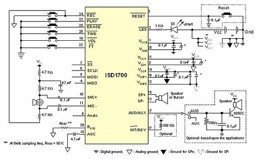
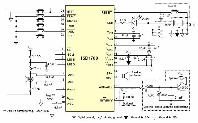
2 1 KΩ FWD LED 19 ** Vcc Gnd VOL V CCD VCCA ** 22 FT VCCD 1 V 0.1 F * VCCD VSSD 28 CCP V 21 VCCA 7 SS CCA 6 V SSA 8 0.1 F * SCLK V CCP 5 V CCP 14 MOSI ISD1700 V 16 µ * * 4 SSP1 0.1 F 0.1 F MISO V 12 SSP2 10 15 Speaker MIC+ SP+ V CC 11 13 or Buzzer Speaker MIC - SP- 0.1 F 9 17 AUD AnaIn AUD/AUX 8050C
40mA inkl. µc! ...waren innerhalb von einer Woche im Kasten! http://www.ebay.de/itm/250992793010?ssPageName=STRK:MEWNX:IT&_trksid=p3984.m1497.l2649 Gruß Michael
Serienmessungen schneller messen wenn man zB. aus einer handvoll Transistoren den mit dem hoechsten ß sucht oder einige Kondensatoren durchmisst, ist das machbar ? vlG Charly
, dass man je nach Hardware (ob Arduino oder ESP) die Standard-SPI-Belegung nimmt (SCK, MISO,MOSIO,SS) und dazu eine CS( Chip select). Ein initiales "Hallo" habe ich nicht gebraucht, irgendwann gings, als ich auf verschiedenen Kanälen gesendet und immer auf 3 gehorcht habe. Und die Sache mit Git:
spannt sie ein WLAN auf. > > Danke Hallo Thomas DTU-Pro hat noch Ethernet(RJ45) und RS485-Modbus SS
Angesichts der Situation in Asien haben wir in der vergangenen Woche in der Vorlesung Analysemöglichkeiten von Krankheitsverläufen und Ausbreitungen besprochen und angewendet. Ich nehme an, in anderen Instituten ist das ähnlich?? Zunächst verlaufen diese bekanntlich exponentiell, bis das Ende der Inkubationszeit erreicht ist und begonnen wird, Maßnahmen zur Eindämmung zu ergreifen, weil alles, was erkannt wird, schon infiziert ist und davon nicht hat profitieren können. Nachdem die Maßnahmen greifen, kommt es zu einem Abknicken. Die Zahl wird dann gesättigt sein und später abklingen, weil dann
Batterieclip und Klappe sind intakt netter Stapel dieser Platinen (neben dem Seitenschneider) mit 8ß0er-Jahre Bauteilen Empfänger für Funkmicros ("The T-Bone") und vieles auch ohne Foto, das immer auch direkt zum Schrotter wandern kann.
900ss schrieb im Beitrag #7996030: > .● Des|ntegrator ●. schrieb im Beitrag #7996011: >> für die man den Webservice abgeschaltet hat > > Der notwendige Logitech-Mediaserver wird weiterhin von freiwilligen
the connectors (SS11 and SS33). 2. Unlock the cable clampers to free the cable. 4. Disconnect the flexible cables (SS53 and SS56). 3. Disconnect the connector (SC2). 5. Disconnect the bridge connector (SS21-SS24). 4. Disconnect
voltage signals applied to liquid crystal. To change the shift direction of signal outputs, use the SS bit. S720~S1 O LCD SS = “0”, the data in the RAM address “h00000” is output from S1. SS = “1”, the data in the RAM address “h00000” is output from S720. S1, S4, S7, … display red (R), S2, S5, S8, ...
voltage signals applied to liquid crystal. To change the shift direction of signal outputs, use the SS bit. S720~S1 O LCD SS = “0”, the data in the RAM address “h00000” is output from S1. SS = “1”, the data in the RAM address “h00000” is output from S720. S1, S4, S7, … display red (R), S2, S5, S8, ...
voltage signals applied to liquid crystal. To change the shift direction of signal outputs, use the SS bit. S720~S1 O LCD SS = “0”, the data in the RAM address “h00000” is output from S1. SS = “1”, the data in the RAM address “h00000” is output from S720. S1, S4, S7, … display red (R), S2, S5, S8, ...
voltage signals applied to liquid crystal. To change the shift direction of signal outputs, use the SS bit. S720~S1 O LCD SS = “0”, the data in the RAM address “h00000” is output from S1. SS = “1”, the data in the RAM address “h00000” is output from S720. S1, S4, S7, … display red (R), S2, S5, S8, ...
voltage signals applied to liquid crystal. To change the shift direction of signal outputs, use the SS bit. S720~S1 O LCD SS = “0”, the data in the RAM address “h00000” is output from S1. SS = “1”, the data in the RAM address “h00000” is output from S720. S1, S4, S7, … display red (R), S2, S5, S8, ...
R01h) R/W RS CB15 CB14 CB13 CB12 CB11 CB10 CB9 CB8 CB7 CB6 CB5 CB4 CB3 CB2 CB1 CB0 W 1 0 0 0 0 0 SM 0 SS 0 0 0 0 0 0 0 0 SS: Shift direction of the source driver output selection. When SS = “0”, source driver shift from S1 to S720. When SS =“1”, source driver shift from S720 to S1. Moreover, SS can cooperate with BGR for different color filter configuration of LCD panel. The combination of SS and BGR bit are summarized at Table 6-2. ★Note: After changing SS bit or BGR bit, display data must be rewritten. Table 6-2 SS=0;BGR=0; S1 S2 S3 S718 S719 S720 SS=0;BGR=1; S1 S2 S3 S718 S719 S720 SS=
must always be DD DDIO DDA SS SSIO SSA connected to the external power supply (2) INJ(PIN)must never be exceeded. This is implicitly insured if VINmaximum is respected. If VINmaximum cannot be respected, the injection current must
No Need WAMPU6 V5.11 CYPRESS MPU/MCU CY7C66013(SSOP48) ADP-CY7C66XX-SS No Need WAMPU6 V5.11 CYPRESS MPU/MCU CY7C66111 ADP-CY7C66XX-SS No Need WAMPU6 V5.11 CYPRESS MPU/MCU CY7C66112 ADP-CY7C66XX-SS No Need WAMPU6 V5.11 CYPRESS MPU/MCU CY7C66113 ADP-CY7C66XX-SS No Need WAMPU6
Fluke 8040 A Digitalmultimeter ISO 148,41 6205 Fluke 8042 A Digitalmultimeter ISO 148,41 6206 Fluke 8050 A Digitalmultimeter ISO 56,70 6207 Fluke 8060 A Digitalmultimeter ISO 56,70 6208 Fluke 8062 A Digitalmultimeter ISO 56,70 6209 Fluke 80i-1010 Strommesszange ISO 56,70 6212 Fluke 80i-400 Strommesszange
84 Y3 A3 QR4 FROM ~···-~~\P963[>P93317P3501 Iio.NOTCH @ A B S · VHS/ON L- ~ +- D ~ SYSTEM CTL 8 " ss ss r (b) L - ~D- -Cl~ EXCLUSIVE OR GATE ~D- r<J~ L H 82 H H 911' 8 MOTHER G.B. A P6003 P963 P933 P3501 H.SW D3 ,--L, I P6002 P962 P933 P3501 I REF N0.351l0 SERIES SYSTEM CTL 2 17 168 168 ROTARY SW L-
+1.05V_RUN_SL585_IO C 4 7 9 5 8 C U701 2 1 2 1 5 1 1 VGA 27M R706 R710 U C E T 2 I I C S R D D C U SS DY Mount D D D D D R P D D D D V _ _ NON-SS Mount DY A00-0104-1 V V V V D D +3.3V_RUN_SL585 V V 2 RN701 2 3 CLK_MCH_DREFCLK1# 4 6 CLK_27M R706 2 1 33R2J-2-GP CLK_VGA_27M [81] VR_CLKEN# [47] [23] DREFCLK# 0R4P2R-PAD 1 4 CLK_MCH_DREFCLK1 3 DOT_96# 27MHZ 7 CLK_27M_SS R710 2 DY 1 33R2J-2-GP R705 [23] DREFCLK DOT_96 27MHZ_SS DY 10KR2J-3-GP G RN702 2 R 3 CLK_IN_DMI# 14 +3.3V_RUN [23] CLKIN_DMI# 0R4P2R-PAD 1 N 4 CLK_IN_DMI 13 SRC_2# 16 CPU_STOP# R701 2 1 2K2R2J-2-GP

 Bild
Bild
 Bild
Bild
 Bild
Bild
 Bild
Bild
 Bild
Bild
 Bild
Bild