F F n M Class-E circuits have operated at m s - n F F n n - i e s s e u h u u a ) 5 frequencies as high as 8.35-10 GHz A a s e S S e c s m m A A m j y j j h i2 e T p I M M I S p c S G G S F R F F A d1 (Reference
unless otherwise specified. amb Symbol Parameter Conditions Min Typ Max Unit VF forward voltage IF= 0.1 mA [1] - 90 130 mV IF= 1 mA [1] - 150 190 mV IF= 10 mA [1] - 210 240 mV IF= 100 mA [1] - 280 330 mV IF= 500 mA [1] - 355 390 mV IF= 1000 mA; T amb = 25 °C [1] - 420 500 mV R reverse current V R 10 V [1
unless otherwise specified. amb Symbol Parameter Conditions Min Typ Max Unit VF forward voltage IF= 0.1 mA [1] - 90 130 mV IF= 1 mA [1] - 150 190 mV IF= 10 mA [1] - 210 240 mV IF= 100 mA [1] - 280 330 mV IF= 500 mA [1] - 355 390 mV IF= 1000 mA; T amb = 25 °C [1] - 420 500 mV R reverse current V R 10 V [1
NUMBER OF TIME TIME TIME WD1 WD0 INTERVAL CLOCKS @ 1.8432 MHZ @ 10 MHZ @ 25 MHZ 17 0 0 2 131072 71.11 mS 13.11 mS 5.24 mS 20 0 1 2 1048576 568.89 mS 104.86 mS 41.94 mS 23 1 0 2 8388608 4551.11 mS 838.86 mS 335.54 mS 1 1 26 67108864 36408.88 mS 6710.89 mS 2684.35 mS 2 The Watchdog timer will de disabled
Measured Calculated (AAC Voltage in Resistance in (V) (Ω) PE – terminal to enclosure cover 1 26,1A 1,9V 72mΩ PE – terminal to enclosure cover 2 26,1A 2,1V 80mΩ PE – terminal to enclosure heatsink 26,1A 1,9V 72mΩ PE – terminal to enclosure side 26,1A 2,0V 77mΩ ES 5000 Accessible conductive part Test current
M.M.M schrieb im Beitrag #7082719: > Millimeterpapier ist nicht verzerrt noch hat es eine über die Blattgröße > gemessene erkennbare Ungenauigkeit. Außerdem spielt eine gleichmäßige Verzerrung keine
M.M.M schrieb im Beitrag #7085216: > Elektrixer schrieb: >> Vor 30 Jahren >> war das vielleicht noch mehr ein Thema weil das Internet noch keine >> alltägliche Anwendung war und nur wenige Studenten
#7081090: > Tantal würde ich nicht verwenden, da der Innenwiderstand zu groß sein > könnte. Bei 10 mA Laststrom kann der Innenwiderstand 1 Ohm sein und es fallen trotzdem nur 10mV an ihm ab...
oder evtl. ein kleiner Akku: https://eckstein-shop.de/LiPoAkkuLithium-IonPolymerBatterie32C7V350mAhJST-PHConnector https://eckstein-shop.de/LiPoAkkuLithium-IonPolymerBatterie32C7V150mAhJST-PHConnector
Messingstecker aufbiegen ist nicht sehr haltbar. Messingrohr MS63 2,5x0,45mm 1,6mm innen 1m lang für 2,99 https://www.fechtner-modellbau.de/material/messing-profile/rund-rohre/8193/messingrohr-ms63-2-5x0-45mm-1-6mm-innen-1m-lang aufbohren auf Innendurchmesser 2,0, ggf. schlitzen 25 Messing-Hohlnieten
und mit 2,0mm bohren z.B. Pomona Model 3690 Miniature Solder Type Banana Plug Fits miniature 0.104in (2.64mm) dia. banana jacks https://www.pomonaelectronics.com/products/hardware/miniature-banana-plug-do-it-yourself https://www.pomonaelectronics.com/sites/default/files/d3690_4617_1_02_0.pdf
/ [ / 45 / ] ] ]S 1 [ [ EE E E A D DC I [ [ 7 T R X X LK O S A L/ S I O ] _D 9 3 N NE E N N E_ [ R M R 11 A [ [ [B C M M CC C C T ]] E ] T T 1 IC9 GND 1 1 ] ] SS I O S /D / / / [ X] 0 0 ] ]/ [ ] ] EE M P W W MM C M P P] ] W W RR R R I [2 N 1 M M P MIC5205 -4.0YM +4V_SWI R / 0 [ /K / / 2 2T D S D P S2
G O 4 G G G G G G I 1 1 1 1 1 1 1 1 9 8 7 6 4 3 2 11 1 1 1 1 11 1 9 8 76 5 4 3 2 1 6 3 2 M M M M M M M M M M M M M M M MM M M M M MM M M M MM M M M M M 2 2 2 2 2 2 2 2 2 2 2 2 2 2 2 21 1 1 1 1 11 1 1 1 11 1 1 1 1 1 C36 F F F F F F F F F F F F F F F FF F F F F FF F F F FF F F F F F 100n C .
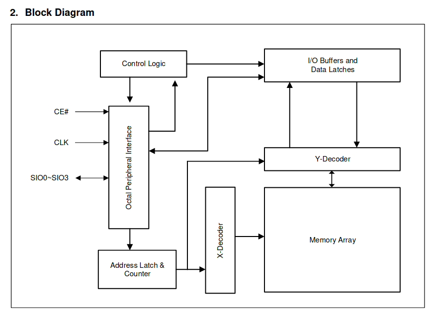 (Bildquelle: ISSI) Eine 32Mbit-Variante des Bausteins (IS66WVS4M8ALL-104NLI) kostet in Hunderterstückzahlen rund 2.5 EUR; als Gehäuse kommt SOIC 150mil zum Einsatz. Es gibt auch Varianten mit 8 und 16 Mbit. ### Digilent MCC E-1608: Datenerfassung per Ethernet
attachment/558058/7.png) (Bildquelle: Mill-Max) Als maximalen Kontaktwiderstand verspricht man 30 mΩ, in Sachen Spannung wird 100 VRMS/150 VDC angeführt. Interessant ist auch die Qualifikation der Steckverbinder im Bezug auf Vibration. Angemerkt sei allerdings, dass die Konnektoren alles andere als
Max M. schrieb im Beitrag #7071919: > Eines der zahlreichen 8051 Derivate. Z.B. der DS80C390 kann 4MB direkt adressieren und hat 4kB Stack.
Bei PIC24 gibt es auch Derivate mit Par-IF (EPMP), aber 5 V-UB sind da die Ausnahme. Renesas M16C..M32C, R32C haben auch Par-IF, und 5 V-UB, sind aber schon älter. Renesas RX (Flash-max-120MHz) gibt es damit auch, einige auch mit 5 V-UB. Von Arm-CM3 gibt es wohl auch ein paar Hersteller mit
OUT = V CC 2 mA IDSS Leakage current EN = low; OUT = GND -0.3 mA Source drain diodes V Forward ON voltage I = 1.4 A, EN = low 1.15 1.3 V SD SD t Reverse recovery time I = 1.4 A 300 ns rr f t Forward recovery time 200
voltage should not exceed the rated voltage of MLCC." In diesem Murata Datenblatt zum GRJ32DR72E104KWJ1 finden sich diese und weitere Angaben auf Seite 8 unter Rating - 3.Applied Voltage https://eu.mouser.com/datasheet/2/281/GRJ32DR72E104KWJ1_01-1978049.pdf Im Samsung Datenblatt zu ihren MLCC
Und auch Kemet K-Sim bestätikt den Faktor 2*sqrt(2). Für den 100nF 250V X7R C1206C104KARAC bis etwa 1,8 kHz https://ksim3.kemet.com/share/421726ee3bbe48c983bf185fd98a63c5
Wenn ich das Gerät 10 Jahre einsetzen möchte (87k Stunden) ergibt das mit dem Strom von 1uA rund 87mAh die ich brauche. Jörg R. schrieb im Beitrag #7070200: > Mit 30mAh eine Alternative zur CR2032 mit ca. 220mAh? Im Ernst? Muss man 220mAh vorhalten, wo selbst 100mAh ausreichend sind?
Operator S. schrieb im Beitrag #7070542: > Jörg R. schrieb: >> Mit 30mAh eine Alternative zur CR2032 mit ca. 220mAh? Im Ernst? > Muss man 220mAh vorhalten, wo selbst 100mAh ausreichend sind? Nein, muss man nicht. Nur hast Du bis zu diesem Kommentar keinerlei Angaben
1000μF ) 1 ) 1 SE ( % N N + + in= 20kHz in= 20Hz H D T A = 0dB T 0.1 V 0.1 AV= 14dB fin 1kHz 0.010 40m 80m 120m 160m 200m 240m 0.0110m 50m 100m 200m 300m Output Power (W) Output Power (W) THD+Nvs.Frequency THD+Nvs.Frequency 10 10 VDD5V V =5V R =16Ω A =0dB L V PO=125mW R L16Ω ) CO=1000μF C O1000μF ( 1
Parameter Test Conditions Min. Typ. Max. Unit V s Supply Voltage 12 36 48 V Vref Reference Voltage IREF= 2mA 13.5 V REF Output Current 2 mA s Quiescent Supply Current EN = H V INL 10 15 mA EN = H V IN= H L = 0 10 15 mA EN = L ( Fig. 1,2,3) 8 15 mA f Commutation Frequency (*) 30 100 KHz c Tj Thermal Shutdown
vor Benutzung per Datenbus programmieren musst: https://www.pollin.de/p/alps-uhf-modulator-mdlp3w104a-605067 Sonst sind fast nur noch Lösungen für CATV Systeme zu haben, die recht teuer sind. Du bist halt einfach 20 Jahre zu spät dran mit deinem Wunsch.
Soso. https://de.m.wikipedia.org/wiki/Satellite_Based_Augmentation_System Sbas?... Ja sicher dat. Der PI kann Composite, also FBAS. Kurzform für Farb-, Bild-, Austast- und Synchronsignal. Alle Bestandteile eines normgerechten
16bit MCU mit DSP á 2,50€ TMS320LF2406 DSP, DSC 16-Bit Fixed-Pt DSP with Flash á 3,00€ MT48LC32M16A2P-75 DRAM 512Mb, 3.3v, 133Mhz 32M x 16 SDR á 1,00€ ATMega2580-16AU 8-Bit-ATMega, 256 KB, 16 MHz, TQFP-100 á 5,00€ ISPLSI2032VE In-System Programmable High Density PLD á 0,50 EP1C3T144C8N FPGA Cyclone I291 LABs 104IOs á 0,50 XR16L2550IM-F UART-IC-Interface 2.5V-5.5V 16B FIFO á 0,50€ AT89S8252 8-Bit uController 8KB Flash á 0,50€ [/pre] alle neu abr etwas älter, versenden zu Selbstkosten
interessieren? Ich mach mal eine kleine Liste an den Bauteilen: L1 (Spule MAX1688): SPM7054VT-100M-D C1,C22 (100nF Eingangskondensatoren): C0805C104K5RAC7411 C2 (47uF Eingangskondensator): F981A476MSAAS1 C3,C23 (1000uF): EEH-ZS1E102UV
musst Du prüfen. Man erkannt LTE Modem mit GPS meist an den drei Anschlüssen. Falls es ein LTE CAT M1 Modem sein darf, geht auch das BG96 MiniPCI-E von Quectel. Gab es vor der Krise <20€. Braucht aber einen Vertrag, der Cat M1 kann. Dafür sehr sparsam im Energieverbrauch.
Elektronikladen, hier ein Nachfolger http://amidon.de/contents/de/d232.html aber das hat sie nach Gewinde M3 und M4 sortiert und nichts vorrätig https://neosid.de/import-data/product-pdf/neoFilterspReihe5-7-10.pdf Neosid hat noch abgleichbare Filterbausätze, aber 7mm ist schon recht groß. https://www.box73.de/index.php?cPath=82_104 auch im "Funkamateur"-Shop gibt es die Filterbausätze, aber wie gesagt 7mm ist schon groß. https://vintage-elektronik.de/epages/0a362980-43ba-46fe-827e-e7a7dd62eac4.sf/de_DE/?ObjectPath=/Shops/0a362980
shown in Figure 3-6. ABEL-HDL Reference Manual 104 CPLD Design Strategies "declarations A, B, C, D, E pin; X, Y pin; M node; equations "intermediate signal equations M = A&B&C; X = M # (B$C); Y = (A&D) # (A&E) # M; Figure 3-5. Declarations and Equations Figure 3-6. Schematic with Intermediate Signal M Both design descriptions are functionally the same. Without the intermediate signal, compilation generates the AND gate associated with A&B&C twice, and the device compiler must filter out the common
left_extruder_temperature_raft0: 0 ;right_extruder_temperature_reset: ;left_extruder_temperature_reset: ;start gcode N1 M118 X65.00 Y25.00 Z20.07 T0 M140 S50 T0 M104 S220 T0 M104 S0 T1 N5 M107 N6 G90 N7 G28 N8 M132 X Y Z A B N9 G1 Z50.000 F420 Ich sehe da keine "Funktion" oder Text-Befehle wie /N etc. Das
at 32 BREAKPOINT REGISTER STRUCTURE user definable points (breakpoints) that occur roughly every 37mV. This allows the device to approximate a Break Point Voltage Field wide range of charging lines; it is not limited to constanthe break point voltage field specifies the range of bat- current or even
Symbol Min. Typ. Max. Unit Test condition V - 550 - G - 1700 - Luminous Intensity Iv B - 300 - mcd F =20mA W - 2500 - V 615 - 630 Dominant Wavelength λd G 520 - 535 nm F =20mA B 460 - 475 x 0.25 Color Coordinate F =20mA y 0.25 ViewAngle 2θ 1/2 - 120 - deg F =20mA Electrical Characteristics (Ta=25℃;VDD=
5V5 Pin 1 - 6: IA2A 1206 0603 PA2A IC2C 1206 0603 PC2C NIADC 2242 R23 0603 ADCD 2 CD E N1 11 1 M M M M M M M MX0 0 X X X X X DC 5VP I U 1 0 8 2 ESCLC PIJ3034 PIJ904DA I2C Interface PIR19PIP0902 PIR201 PIR21PI60102 PIR201 PI0603IR1401 PIR2301 GND SS A GWWMWMWMP P P P P P P PB TR T RT R SS PA0P I
l 4 11 mA VOUT Current Limit VOUT = 0V l 2.8 4.5 7 mA VSTORE Current Limit VSTORE = 0V l 2.8 4.5 7 mA VAUX Clamp Voltage Current into VAUX = 5mA l 5 5.25 5.55 V VSTORE Leakage Current VSTORE = 5V 0.1 0.3 μA VOUT2
Symbol Parameter and Test Condition Frequency Units Min. Typ. Max. σ d test Current drawn N/A mA 45 53 65 3.57 NF[1] Noise Figure 1.9 GHz dB 1.9 2.3 0.15 0.9 GHz 1.8 Gain[1] Gain 1.9 GHz dB 13 14.2 15.5 0.26 0.9 GHz 15 [1] IIP3 Input Third Order Intercept Point 1.9 GHz dBm 14 +17.5 2.28 0.9 GHz
Package BGA427 BMs 1, IN 2, GND 3, +V 4, Out SOT343 Maximum Ratings Parameter Symbol Value Unit 25 mA Device current ID Device voltage V ,+V 6 V D Total power dissipation Ptot 150 mW TS= 120 °C RF input power PRFin -10 dBm Junction temperature T 150 °C j Ambient temperature range TA -65 ... 150 Storage
high voltage V SR 0.8 V V + 0.5 V – IHS CC CC (Special Threshold) – 0.2 Input Hysteresis HYS 400 – mV – (Special Threshold) Output low voltage VOL CC – 0.45 V IOL= 2.4 mA (PORT0, PORT1, Port 4, ALE, RD , WR, BHE, CLKOUT, RSTOUT) Output low voltage VOL1 CC – 0.45 V IOL1= 1.6 mA (all other outputs) Output
" -larm_cortexM3l_math -lm arm-none-eabi-gcc: error: build/startup_stm32f103x6.o: No such file or directory make: *** [makefile:39: LishuiFOC_01.elf] Error 1 Error: Process completed with exit code 2.[/] Das wird
Lothar M. schrieb im Beitrag #7032206: > In der Praxis hilft das aber nichts, weil die Pegel von '0' und '1' > invertiert sind Doch, schon. Einige MCs können IOs umpolen. Oder als SW-UART geht das auch,
den µs? Probier es mit halbwegs plausiblen Daten: 0 - 1/4 - 3/4 - 1 also 0 - 26 - 79 - 104 µs, oder 0 - 1/3 - 2/4 - 1 also 0 µs, 35 µs, 70 µs, 104 µs Wenn das Bild nichts aussagt, variierst du die Werte. Da kann man sich doch mit den vorgegebenen Eckwerten rantasten... Oder.
}G1 Z{z_offset+min(max_layer_z+70, max_print_height-10)} F600{endif} ; Move print head further up\nM140 S0 ; turn off heatbed\nM104 S0 ; turn off temperature\nM107 ; turn off fan\nM84 X Y E ; disable motors ensure_vertical_shell_thickness = 1 external_perimeter_extrusion_width = 0.45 external_perimeter_speed
50 m 0,0265 mm² / m h 1,7 Ω 4 mm 2 0,02214 mm² / m 2 i 5 Ω 300 m 1,5 mm j 100 cm 2,5 mm2 0,01786 mm² / m k 4 Ω 3000 mm 0,0265 mm² / m l 1,9 mΩ 16 mm 2 0,01786 mm² / m m 50 mΩ 200 mm 1,5 mm2 n 3 µm 0,003 mm2 0,02214 mm² / m o 7 mm 0,03 mm 2 0,0265 mm² / m 2 p 5 m 1 cm 0,01786 mm² / m q 50 m 2 cm2 0,01786 mm² / m 2 r 4 mΩ 4 cm 0,01786 mm² / m s 50 mΩ 3 cm2 0,01786 mm² / m t 30 mΩ 2 cm2 0,01786 mm² / m 2 u 150
AVR1301: Using the XMEGA DAC Features 8-bit • 12 bit resolution Microcontrollers • Up to 1 M conversions per second • Continuous drive or sample-and-hold output • Built-in offset and gain calibration • High drive capabilities • Driver source code included Application Note 1 Introduction The
V DC 1.3 A DC 100 V DC Also, in order to maintain stability of internal IC operation, maintain AQZ 104 400 V DC 0.7 A DC 200 V DC an input current of at least 5 mA (Latch type), 10 mA (Non Latch AQZ 202 PeakAC, DC60V PeakAC, DC3.0A 12 V AC type). 5, 12, 24 V DC 24 V AC AC/ AQZ 205 PeakAC, DC100V PeakAC
