ist entsprechend dem Anschlussplan anzuschliessen. s r t a o s a T n d e w e l c n e h n s t g c o n z k u u c n g t n S i e L f a a s d g n u t l e s a h c e d s - e n e e t h e t g S A c 1 r c i e 2 n T t a e B i l 0 h l r g : s 1 e f e n i n E f h w t w r D u r c i T V A D A
pin 7 (VDD). Connection Diagrams with Auxiliary Interface SPI 3-wire SCK ASDA to BMM A ASCL C S X L SDO 1 12 11 10 CSB CS MOSI MISO SDX 2 BMA456 9 GND 100nF VDDIO VDDIO 3 Top View 8 GNDIO (Pads not visible!) ASDA 4 5 6 7 VDD VDD 1 2 100nF N N I I GND INT1 INT2 It is recommended to use 100nF decoupling
- Relative Reverse Light Current vs. Ambient Temperature 0° 10° 20° 100 30° ) µ t t e s 40° r 10 e 1.0 C I h e i t 0.9 50° L l s V = 5 V R 0.8 60° e 1.0 CE l e λ = 950 nm r R I 0.7 70° -r 80° I 0.1 0.6 0.4 0.2 0 0.2 0.4 0.6 0.01 0.1 1 10 18234 16055 E - Irradiance (mW/cm²) e Fig. 6 - Relative Radiant
habe ich seit gut 25 Jahren privat nur noch Linux. Mit freundlichem Gruß: Bernd Wiebus alias dl1eic http://www.l02.de
H. H. schrieb im Beitrag #7851123: > Route_66 H. schrieb im Beitrag #7851120: >> unerfahrenen jugendlichen Schreiberlinge hier. > > Bist du Methusalem? Für manch einen sind 65 Jährige Personen
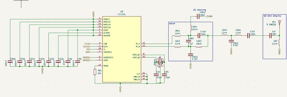
in meinem Plan, inklusive der Anordnung nahe den Pins. Allerdings sind just diese Teile (C7, C10, C11, FB1) auf meiner Platine nicht bestückt. Vermutlich hatte JLCPCB die gerade nicht parat und ich habe das beim Bestätigen der Stückliste übersehen. Außer FB1 (FerriteBead), da war das Absicht, weil ich
auch der Chip kaputtgehen, denn es wird in den Moin moin, Also ich habe die beiden fehlenden 1uF-Kondensatoren C7 und C10 und den Ferritkern FB1 ergänzt. C11 (10nF) war doch schon bestückt. Jetzt hat also VDDA also die vorgesehene Versorgung. Und jetzt funktioniert PLL ganz normal, d.h. ich
-11-2-24-art-3082735 Beide Regelungen ergaenzen sich gegenseitig.
H. H. schrieb im Beitrag #7851477: > Dieter D. schrieb: >> Nix fachlich beigetragen, > > Du ja auch nicht, sogar niemals. Richtig ;-) Was für eine Pfeife
+ 2 mm 18.4 mm 2000 14 | Version 1.6 | 2024-12-06 SFH 3410 DATASHEET Barcode-Product-Label (BPL) 5) Dry Packing Process and Materials Moisture-sensitivelabelorprint LE L E V be dnoalH ). Iba rfit (R . Barcodelabel m i R H e h u e 6 0%
1 VSS 35.98(PLZ) 0.70 30.00 AA 1.10 2 VCC 3 VCOMH 4 VCI 5 VDD Cover Glass 6 BS1 BS2 7 s R 6 8 VSS l G ) r Z A 9 IREF 2 e P A . v ( 10 CS# 0 o 3 0 . 3 C . . 9 2 3 5 0 11 RES# . . 3 3 4 6 12 D/C 3 Pull tape
Stefan H. schrieb im Beitrag #7849653: > René H. schrieb im Beitrag #7849605: >> Mit der richtigen Idee kann man auch richtig gut verdienen. > > Mit welcher Idee hast Du richtig gut verdient? Wer spricht
#7851551: > Gerade Betriebsstoffe fürs Auto darf man ausdrücklich dort lagern. Begrenzt auf 20l Benzin und 200l Diesel, auch das ist in den Garagenverordnungen geregelt.
. Unclatped Inductive load test switching and diode recovery times lercuit o b s D A A A O L G D.U.T. DIODE L=100µH - VD 2200 3.3 S B 3.3 s 1000 µF µF VDD 2Ω B B D c µt( µF DD ID G u RG oS d V i D.U.T. r P P w t e AM01470v1 AM01471v1 le Figuse 20. Unclamped inductive waveform Figure 21. Switching
noch als Pullup, oder Basiswiderstand > verheizen, In der E24 gibt das keine 10,2k, die geht 9k1 - 10k - 11k. Sherlock schrieb im Beitrag #7848957: > Ich habe meine Vorräte sogar auf E3 reduziert. > > Durch zunehmende Digitalisierung braucht man nicht mehr so viele fein > abgestufte Bauteile
Widerstands-Set incl. Versand verlangst. 15 Euro inklusive Versand, das wären dann 85 Werte an Widerständen 1 Ohm bis 10 MOhm (E12 komplett) und 25 Werte Kondensatoren (0.5 1 1.2 1.5 1.8 2.2 2.7 3.3 3.9 4.7 5.6 6.8 8.2 10 12 15 18 33 56 100 330 Piko und 1 3.3 10 100 Nano). Die Cs sind 50V bis auf 100nF der ist
74HC175; 74HCT175 Quad D-type flip-flop with reset; positive-edge trigger 6. Functional description [1] Table 3. Function table Operating modes Inputs Outputs MR CP Dn Qn Qn reset (clear) L X X L H load “1” H h H L load “0” H l L H [1] H = HIGH voltage level; h = HIGH voltage level one set-up time
74HCT138 3-to-8 line decoder/demultiplexer; inverting 6. Functional description Table 3. Function table H = HIGH voltage level; L = LOW voltage level; X = don’t care. Control Input Output E1 E2 E3 A2 A1 A0 Y7 Y6 Y5 Y4 Y3 Y2 Y1 Y0 H X X X X X H H H H H H H H X H X X X L L L H L L L H H H H H H H L L L H H
; X = don’t care; ↑ = LOW-to-HIGH transitionn+1= state after the next LOW-to-HIGH CP transition. Input Output nSD nRD nCP nD nQ nQ n+1 n+1 H H ↑ L L H H H ↑ H H L 7. Limiting values Table 5. Limiting values In accordance with the Absolute Maximum
Nexperia B.V. 2017. All rights reserved Product data sheet Rev. 6 — 19 November 2015 2 of 14 Nexperia 74HC11; 74HCT11 Triple 3-input AND gate 6. Functional description Table 3. Function selection[1] Input Output nA nB nC nY L X X L X L X L X X L L H H H H [1] H = HIGH voltage level; L = LOW voltage level; X
Product data sheet Rev. 7 — 16 April 2020 7 / 14 Nexperia 74HC08; 74HCT08 Quad 2-input AND gate 11. Package outline SO14: plastic small outline package; 14 leads; body width 3.9 mm SOT108-1 D E A X c y H E v M A Z 14 8 Q A 2 A (A3) A 1 pin 1 index θ Lp 1 7 L e detail X b w M p 0 2.5 5 mm scale DIMENSIONS
Intensity vs. Forward Current Figure 12: Maximum Forward Current vs.Ambient Temperature p 1.4 30 d c 1.2 m 25 - - Y ) T I A 1.0 E N 0 R 20 E 2 U I A 0.8 C S C 15 U E D O I 0.6 L I A B U M A 10 L O 0.4 O V ( L T A 5 A 0.2 X E A R M 0.0 0 0 10 20 30 40 0 10 20 30 40 50 60 70 80 90 FORWARD CURRENT
REVISED MARCH 2015 8.3.3 Address Reference INPUTS 2 I C BUS SLAVE I C BUS SLAVE 8-BIT 8-BIT WRITE A2 A1 A0 READ ADDRESS ADDRESS 65 (decimal), 41 64 (decimal), 40 L L L (hexadecimal) (hexadecimal) L L H 67 (decimal), 43 66 (decimal), 42 (hexadecimal) (hexadecimal) L H L 69 (decimal), 45 68 (decimal), 44
8.6 ... 10.5 E 6.88 ... 8.50 E 8.5 ... 10.4 E 10.6 ... 13.0 F 8.51 ... 10.51 F 10.5 ... 12.9 F 13.1 ... 16.1 G 10.52 ... 13.00 G 13.0 ... 16.0 G 16.2 ... 20.0 H 13.01 ... 16.07 H 16.1 ... 18.4 H 20.1 ... 23.0 I 16.08 ... 19.87 J 19.88 ... 24.56 K 24.57 ... 30.35 L 30.36 ... 37.51 Conditions: 1. V CC
time [12] - 3.45 [4] - 0.9[4] - 0.45 [4] μs 2 . - V nL noise margin at the LOW level for each connected device 0.1V DD - 0.1V DD - 0.1V DD - V b (including hysteresis) s s V nH noise margin at the HIGH level for each connected device 0.2V DD - 0.2V DD -
Packaging Specification located at http://www.microchip.com/packaging 2X 0.10 C A–B D A D NOTE 5 N E 2 E2 E1 E 2X 0.10 C A–B 2X 0.10 C A–B 1 2 NOTE 1 e NX b B 0.25 C A–B D NOTE 5 TOP VIEW 0.10 C C A A2 SEATING PLANE 8X 0.10 C A1 SIDE VIEW 4X ș ș2 h R1 h H R c L ș SEE VIEW C (L1) VIEW A–A 4X 1 ș VIEW C Microchip
OderSogarDirektOhneAbstand. Wird aber nicht gemacht, da es ja das Leerzeichen gibt. In meiner ASCII Tabelle ist zwischen 1Fh und 21h kein Schwarzes Loch. Ich könnte das noch weiter ausführen, soll hier aber auch egal sein. Ich könnte deinen Text auch ohne "u" schreiben und er bleibt trotzdem verständlich. Lothar M. schrieb
0.25 dB. Therefore: L = 20 Hz/5 = 4 Hz (11) H = 20 kHz × 5 = 100 kHz (12) At this point, it is a good idea to ensure that the Gain-Bandwidth Product for the part will provide the designed gain out to the upper 3 dB point
specifications Figure 4. Current sense delay characteristics INPUT CS_DIS LOAD CURRENT SENSE CURRENT tDSENSE2H DSENSE1L tDSENSE1H t DSENSE2L Figure 5. Open-load Off-state delay timing OUTPUT STUCK TO V CC V IN V OUT > VOL VSENSEH V CS DSTKON Figure 6. Switching characteristics VOUT t t Won Woff 90% 80% dV /dt
M I W5.0 + - L S ΩM1 02C Fu022 U H 5 p V V61 1 + - Ω 1 35R L 5 C 0 2 12C Fu022 9 1 5 6 3 R Vk2 Vk2 1 2 1 V Q S Fp0033 Fp0033 T 0012RS + 1 Ωk8.6 2 Ωk7.2 Fu7.4 1 u 2W 51R 31R C 2 K5 + V61 2YC 1YC + 01D 2 RV 4C 8 MΩ 0
20 mA Single Pulse startingjT=25°C; DD=24V E as VIN5V R gen=R IN MINn330; L=50mH 55 mJ Avalanche Energy (see figures 3 & 4) (*) Pulsed: Pulse duration = 300 s, duty cycle 1.5% 4/14 2 VNS1NV04D PROTECTION FEATURES - OVERTEMPERATURE AND SHORT CIRCUIT During normal operation, the
characteristics VOUT t t Won Woff 90% 80% dVOUT/d(on) dV OUT/d(off) t 10% tf r t INPUT d(on) td(off) t Table 11. Truth table Conditions INPUTn OUTPUTn STATUSn (V SD=0V)(1) L L H Normal operation H H H L L H Overtemperature H L L Undervoltage L L X H L X H X H Overload & (no power limitation) Short circuit to GND H Cycling L (power limitation) (2) L H L Output voltage >OL H H H L L H(3) Output current < I OL H H L 1. If theSDis high, the STATUS pin is in a high impedance. 2. The STATUS pin is low with a delay eDSTKONoafter
OLI H He L e t o l Table 13. Electrical transient requirembnts ISO T/R O Test level 7637/1 I II- III IV Delays and impedance Test pulse ( s ) 1 - 25Vc)t - 50V1) - 75V1) - 100V(1) 2ms, 10Ω 2 + 25V(1) + 50V
INn VSTATn V STATn SDL t SDL tDOL(off) DOL(on) Table 12. Truth table Conditions Input Output Sense L L H Normal operation H H H L L H Current limitation H X (Tj< TTSD) H H X (Tj> TTSD) L Overtemperature L L H H L L L L X Undervoltage H L X L L H Overvoltage H L H L H L Output voltage >OL H H H L L H
Negative output voltage clamp L L 0 Doc ID 10896 Rev 4 11/27 Electrical specifications VN920SP-E Table 12. Electrical transient requirements on V CC pin (part 1) ISO T/R Test levels 7637/1 test pulse I II III IV Delays and impedance
vereinnahmten Entgelten berechnete Summe der vom Unternehmer ausgeführten steuerbaren Umsätze im Sinne des § 1 Absatz 1 Nummer 1 abzüglich folgender Umsätze: 1. Umsätze, die nach § 4 Nummer 8 Buchstabe i, Nummer 9 Buchstabe b und Nummer 11 bis 29 steuerfrei sind; 2. Umsätze, die nach § 4 Nummer
H. H. schrieb im Beitrag #7847701: > Kannst du doch leicht prüfen. O.K. Dann wird noch einmal genau gemessen: (Referenzspannung ist Referenz - Anode am IC) 1. Platine Referenzspannung: 2.493V
gemessen: Ungenaue Widerstände... Karsten W. schrieb im Beitrag #7847686: > Die Widerstände sind 1% und diese halten die Toleranz tatsächlich ein. 2.498 / 33(+/-1%) x 33(+/-1%)+100(-/+1%) liefert 9.92 bis 10.22 und nicht 11.609. Steckbrettaufbau ?

 Bild
Bild
 Bild
Bild
 Bild
Bild
 Bild
Bild
 Bild
Bild
 Bild
Bild
 Bild
Bild
 Bild
Bild