-
PDF
US4843344.pdf
have ?rstand sectween thesource oftheMOSFET and thesecond end ondends,the?rstendsbeingcoupledtooutputterminal ofcouplingresistor208andcapacitor210ofthatMOS 36.The MOSFET ispreferablyconnectedasavoltage FET circuitasaMOSFET voltage protector.
in „Hochspannungs OPV Fehler/Vorschlag?“ · Analoge Elektronik und Schaltungstechnik ·
-
PDF
klassed_facharbeit.pdf
Mosfet Klasse-D Verstärker 2003 Simon-Emanuel Waid Seite 19 von 24 Abbildung 39: Der Lowside Mosfet wird zu früh eingeschaltet, dies verursacht eine nicht Abbildung 38. Der Lowside Mosfet wird tollerierbare Stromspitze. ausgeschaltet und der Hi side eingescahltet. Der Ch1: Gatespannung HI-Side Mosfet Vorgang läuft korrekt ab. Ch2: Gatespannung Low-Side Mosfet Ch1: Gatespannung HI-Side Mosfet Ch2: Gatespannung Low-Side Mosfet Abbildung 40: Völlig unkorrektes Umschalten: Der Hiside Mosfet sperrt
in „Suche Schaltplan für PWM Endstufe“ · Mikrocontroller und Digitale Elektronik ·
-
PDF
4412f.pdf
OncetheauxiliaryMOSFEThasturnedonthevoltagedrop loadwillinitiallybepulledupbythedrain-sourcediodeof across it can be very low depending on the MOSFET’s the P-channel MOSFET. As the LTC4412 comes into characteristics. action, it will control the MOSFET’s gate toturnit onand Figure3illustratesanapplicationcircuitfortheautomatic reduce the MOSFET’s
in „Akku_bei_MP3-Player“ · Analoge Elektronik und Schaltungstechnik ·
-
PDF
app-note_HIP_4081A.pdf
pulses exists one BIAS LOWER (12VDC) turn-off pulse. Each time a turn-off pulse is issued to an ALS MOSFET upper MOSFET, the bootstrap capacitor of that MOSFET TO “B-SIDE” OF H-BRIDGE begins its “refresh” cycle. A refresh cycle ends when the VSS SUPPLY upper MOSFET is turned on again, which varies depending
in „HIP 4081 Verständnisprobleme“ · Mikrocontroller und Digitale Elektronik ·
-
PDF
LTC4414_Power_Manegement.pdf
MOSFET. As the LTC4414 comes into switchoverofaloadbetweenabatteryandawalladapter in the comparator mode. It also shows how a battery action, it will control the MOSFET’s gate toturnit onand reduce the MOSFET
in „P-Mosfet als Schalter“ · Analoge Elektronik und Schaltungstechnik ·
-
PDF
MOSFET_oder_bipolarer_Transistor__Zetex.pdf
continued to be developed, and in some applications can be a better choice of power switch than MOSFETs. Device Characteristics Given the preponderance of publicity in favor of MOSFETs it is easy to get the impression that MOSFETs are better in all respects than bipolar transistors. Comparing typical
in „mit 2,7V schalten“ · Mikrocontroller und Digitale Elektronik ·
-
Datei
Phasenabschnitt_10.c
io.h> #include <avr/interrupt.h> #define T_UP PINB0 #define T_DOWN PINB1 #define T_PIN PINB #define MOSFET_DDR DDRD #define MOSFET_PORT PORTD #define MOSFET_PX PD3 #define SET_MOSFET_OUT MOSFET_DDR|=(1<<MOSFET_PX) #define MOSFET_EIN MOSFET_PORT&=~(1<<MOSFET_PX) //LOW -> Mosfet einschalten! #define MOSFET_AUS
in „Phasenabschnittsdimmer“ · Mikrocontroller und Digitale Elektronik ·
-
PDF
PanasonicPhotomosRelayPhotovoltaicMOSFETDriver.pdf
allowed to flow. When the treshold voltage V th reached at t ,1the drain current i Df the power MOSFET increases to a full load current. www.panasonic-electric-works.com Version: 29/06/2005 Subject to change without notice Application Note 031 Photovoltaic MOSFET driver However, the MOSFET has not turned
in „Sicheres Schalten von MOSFET-Relais“ · Analoge Elektronik und Schaltungstechnik ·
-
PDF
Schaltnetzteil-tutorial.pdf
mathematisch eine Gerade, so wie es die Simulation auch zeigt. Schaltung 2 - Induktivität alleine mit MOSFET Bild 3, 4 Hier wird nun kein idealer Schalter verwendet sondern ein Modell eines MOSFET. Die parasitären Eigenschaften des simulierten MOSFET bewirken bereits eine Veränderung der Kurvenformen im Vergleich
in „Art of Electronics 3rd Edition erhältlich“ · Analoge Elektronik und Schaltungstechnik ·
-
PDF
PSpice_LibraryguideOrCAD.pdf
MOSFET IRFF131 IRFF131 PWRMOS.OLB Power MOSFET IRFF132 IRFF132 PWRMOS.OLB Power MOSFET IRFF133 IRFF133 PWRMOS.OLB Power MOSFET IRFF210 IRFF210 PWRMOS.OLB Power MOSFET IRFF211 IRFF211 PWRMOS.OLB Power MOSFET
in „pSpice - Bauteil hinzufügen.“ · Analoge Elektronik und Schaltungstechnik ·
-
Bild
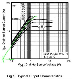
Kennlinie eines MOSFETs
100 TOP 7.00V 5.00V 4.50V 3.50V 3.00V 2.70V 2.50V BOTTOM 2.25V 2.25V 10 ID, Drain-to-Source Current (A) 20µs PULSE WIDTH TJ = 25 °C 1 0.1 VDs, Drain-to-Source Voltage (V) 10 100 Fig 1. Typical Output Characteristics
in „Welcher N-Kanal Mosfet für dieses Projekt?“ · Analoge Elektronik und Schaltungstechnik · · Diagramme
-
Bild
-
Bild
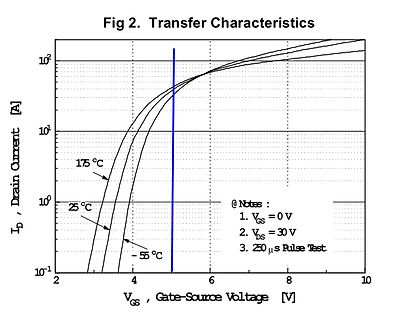
Transferkennlinie eines MOSFETs
Fig 2. Transfer Characteristics ID, Drain Current [A] 10^2 10^1 10^0 10^-1 175 °C 25 °C - 55 °C @ Notes : 1. VGS = 0 V 2. VDS = 30 V 3. 250 µs Pulse Test VGS, Gate-Source Voltage [V]
in „Reverse Voltage Protection“ · Analoge Elektronik und Schaltungstechnik · · Diagramme
-
Bild
Kennlinie eines MOSFETs
1000 VGS TOP 15V 10V 8.0V 7.0V 6.0V 5.5V 5.0V BOTTOM 4.5V ID, Drain-to-Source Current (A) 100 10 4.5V 1 20µs PULSE WIDTH TJ = 25 °C 0.1 1 10 100 VDS, Drain-to-Source Voltage (V)
in „Step-Down-Spannungsregler stört ESP8266 oder MOSFET?“ · Analoge Elektronik und Schaltungstechnik · · Diagramme
-
Bild
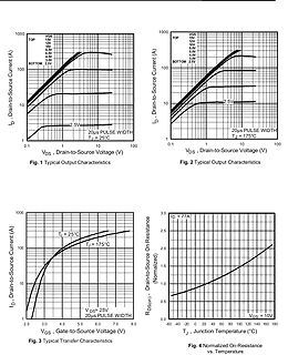
Kennlinien eines MOSFETs
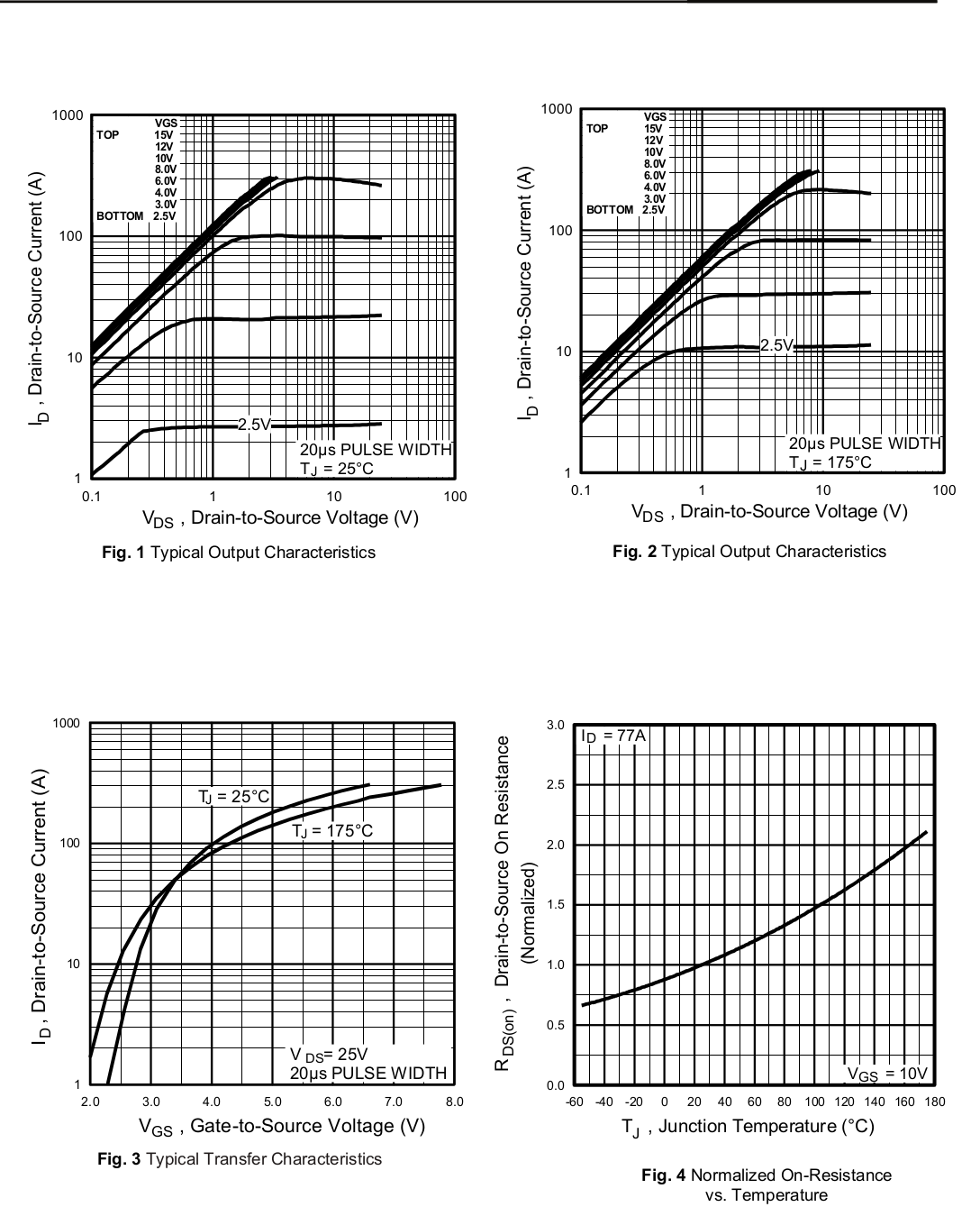
1000 VGS 10V 12V 10V 8.0V 6.0V 4.0V 3.0V 2.5V BOTTOM 100 ID, Drain-to-Source Current (A) 100 10 1 0.1 1 TOP 2.5V 20µs PULSE WIDTH TJ = 25°C Fig. 1 Typical Output Characteristics 1000 VGS 15V 12V 10V 8.0V 6.0V 4.0V 3.0V 2.5V BOTTOM 100 ID, Drain-to-Source Current (A) 100 10 2.5V 1 0.1 1 10 100 1000 VDS, Drain-to-Source Voltage (V) 20µs PULSE WIDTH TJ = 175°C Fig. 2 Typical Output Characteristics 1000 ID, Drain-to-Source Current (A) 100 10 1 TJ = 25°C TJ = 175°C 1 2.0 3.0 VGS, Gate-to-Source Voltage (V) 4.0 5.0 6.0 7.0 8.0 Fig. 3 Typical Transfer Characteristics 3.0 ID = 77A 2.5 2.0 1.5 1.0 0.5 0.0
in „Step-Down-Spannungsregler stört ESP8266 oder MOSFET?“ · Analoge Elektronik und Schaltungstechnik · · Diagramme
-
Bild
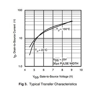
Transferkennlinie eines MOSFETs
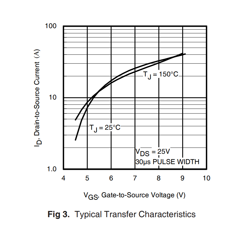
100 ID, Drain-to-Source Current (A) 10 TJ = 150°C TJ = 25°C VDS = 25V 30µs PULSE WIDTH 1.0 4 5 6 7 8 9 10 VGS, Gate-to-Source Voltage (V) Fig 3. Typical Transfer Characteristics
in „Mosfet schaltet nicht "durch"“ · Analoge Elektronik und Schaltungstechnik · · Screenshots
-
Bild
Kennlinie eines MOSFETs
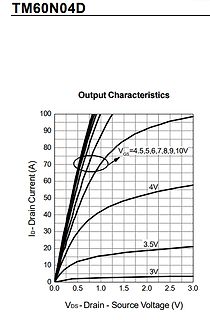
TM60N04D Output Characteristics 100 90 80 70 60 50 40 30 20 10 0 Id - Drain Current (A) 0.0 0.5 1.0 1.5 2.0 2.5 3.0 VDS - Drain - Source Voltage (V) VGS=4.5,5,6,7,8,9,10V 4V 3.5V 3V
in „RPi pico PWM Ansteuerung 24V“ · Mikrocontroller und Digitale Elektronik · · Screenshots
-
Bild
MOSFETs auf Kühlkörper
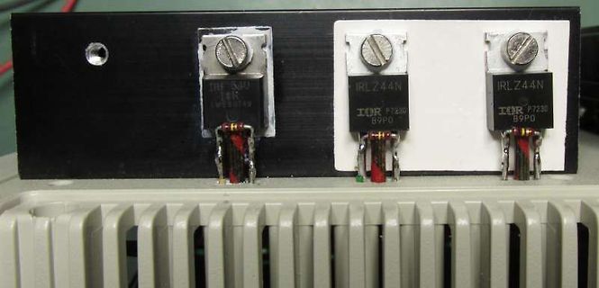
IRLZ44N IR P7230 89P0
in „Kapazität eines NiMH Akku ermitteln“ · Analoge Elektronik und Schaltungstechnik · · Fotos
-
Bild
Transferkennlinie eines MOSFETs
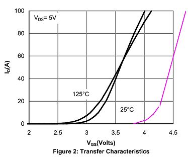
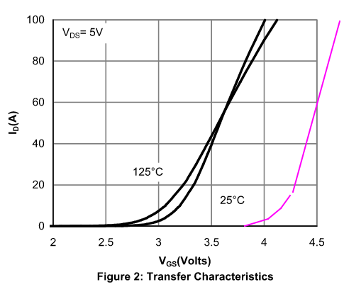
100 VDs=5V 80 ID(A) 60 125°C 40 25°C 20 0 2 2.5 3 3.5 4 4.5 VGS(Volts) Figure 2: Transfer Characteristics
in „Transistor für Bewegungsmelder“ · Analoge Elektronik und Schaltungstechnik · · Diagramme
-
Bild
Kennlinie eines MOSFETs
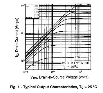
10^2 TOF 15V 10.0V 7.0V 5.5V 5.0V 4.5V BOTTOM ID, Drain Current (Amps) 10^1 10^0 4.5V 20us PULSE WIDTH TC = 25°C 10^-1 10^0 10^1 VDS, Drain-to-Source Voltage (volts) Fig. 1 - Typical Output Characteristics, TC = 25 °C
in „Betrieb einer HighPower IR LED an einem Arduino“ · Analoge Elektronik und Schaltungstechnik · · Diagramme
-
Bild
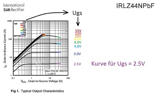
Kennlinie eines MOSFETs
International IOR Rectifier IRLZ44NPbF Ugs 15V 12V 10V 9.0V 6.0V 5.0V 4.0V 3.0V 2.5V TOP BOTTOM ID, Drain-to-Source Current (A) VDS, Drain-to-Source Voltage (V) 20µs PULSE WIDTH TJ = 25°C Kurve für Ugs = 2.5V Fig 1. Typical Output Characteristics
in „ESP32 mit 3,3V PWM einen 3,7V Motor betreiben“ · Analoge Elektronik und Schaltungstechnik · · Diagramme
-
PDF
AN11158_Understanding_MOSFET_data_sheet_parameters__NXP.pdf
AN11158 Understanding power MOSFET data sheet parameters Rev. 3 — 7 January 2013 Application note Document information Info Content Keywords MOSFET. Abstract This application note describes the content of power MOSFET data sheet parameters
in „Flyback-Wandler Störungen auf Versorgung“ · Analoge Elektronik und Schaltungstechnik ·
-
PDF
MP6528.pdf
5V TO 60V, H-BRIDGE GATE DRIVER APPLICATIONS INFORMATION Related to the current capability of the MOSFET is the rds(on). This is the resistance of the VIN Input Voltage MOSFET when it is in the fully “turned on” state. The MOSFET will dissipate power proportional to The VIN pin supplies all power to the
in „H-Brücke 48V, PWM 50kHz, Möglichkeit 100% Duty Cycle on“ · Analoge Elektronik und Schaltungstechnik ·
-
PDF
MOSFET_Switched_Mode_Amplifiers_Part_1_-_Handimans_Guide.pdf
dynamic range. A floored to find out QRPers were using graph showing these regions is called MeettheMOSFET current and heating of the mosfet – and them at 7MHz or higher. I faxed them the "transfer characteristics" of a often failure. If you haven't blown up an device, as illustrated in Fig. 1A, MOSFET's
-
PDF
Beschreibung_KFZ_Softstartmodul_mit_FET.pdf
). Ab einer Spannung von ca. 4 V unter +Ub beginnen die MOSFETs langsam zu leiten. Im Bereich von -4 V bis -6 V steuern die MOSFETs dann immer weiter durch. Ab -7 V und weniger (fast Masse) sind die MOSFETs gesättigt und voll durch gesteuert. Der eigentliche Übergangsbereich
in „Softstart für H7 Leuchtmittel im PKW“ · Mikrocontroller und Digitale Elektronik ·
-
PDF
ZXGD3105EV1_User_Guide_Issue_1..pdf
senses the forward voltage drop of the parasitic diode within the MOSFET, and when the diode is in conduction, applies a voltage to the MOSFET gate, turning on the MOSFET after an initial delay time. The gate output voltage of the controller is then proportional to the
in „SPICE Model einbindung problem“ · Analoge Elektronik und Schaltungstechnik ·
-
PDF
3703fc.pdf
). Percent output voltage. When this condition is sensed the top efficiency can be expressed as: MOSFET is turned off and the bottom MOSFET is forced on. The bottomMOSFET remains on continuously for as %Efficiency = 100%– (L1 + L2 + L3 + ...) longasthe0Vconditionpersists;ifV OUT returnstoasafe whereL1
in „Längs- oder Querregler 40V 250W als Überspannungsschutz für Tiefstellsetzer“ · Analoge Elektronik und Schaltungstechnik ·
-
PDF
fetdrvr-t.pdf
converters. In its present form, this driver is quite suitable to oper- 14 140 12 I in (mA) 120 Mosfet Drain V 5pF mA Mosfet Gate 10 Vpk Out 100 Gate driver input (Volts) 2.5pF 8 80 5V/div Gnd 1pF Gnd 2V/div 6 60 1pF 4 40 2.5pF Mosfet Drain I in 2 5pF 20 Mosfet Gate 0 2 3 4 5 6 70 Gate driver input
in „Ansteuerung H-Vollbrücke“ · Analoge Elektronik und Schaltungstechnik ·
-
PDF
DRF1200_06102008.pdf
Application Note 13.56 MHz, CLASS-E, 1KW RF Generator using a Microsemi DRF1200 Driver/MOSFET Hybrid March 28, 2008 By Gui Choi Sr. Application Engineer 1 http://www.microsemi.com Microsemi PPG 13.56MHz 1KW RF Generator Application Note with DRF1200 Driver/MOSFET Hybrid Contents 1. INTRODUCTION
in „Bauplan für HF Netzteil gesucht.“ · HF, Funk und Felder ·
-
PDF
ALD110800-1489.pdf
(quad/dual) are EPAD MOSFETs in The turn-on and turn-off electrical characteristics of the EPAD MOSFET products are shown in the Drain-Source On Current vs which the individual threshold voltage of each MOSFET is fixed at Drain-Source
in „Radiobasteln - Was hat 2018 noch Aussicht auf Erfolg ?“ · HF, Funk und Felder ·
-
PDF
A4989-Datasheet-1.pdf
MOSFETs. External series MS1 and MS2 These Microstep Select inputs are used gate resistors (as close as possible to the MOSFET gate) can be used to reduce the slew rate seen at the gate, thereby to select
in „Masseflächen?“ · Platinen ·
-
PDF
drv8350f_7_.pdf
protection feature. On hardware interface devices, the GDUV protection is always enabled. 8.3.5.3 MOSFET V Overcurrent Protection (VDS_OCP) DS A MOSFET overcurrent event is sensed by monitoring the V voltage drop across the external MOSFET DS RDS(on) If the voltage across an enabled MOSFET exceeds the
in „BLDC-Motor: Überspannung beim Bremsen trotz Durchschaltung aller Low-Side-MOSFETs?“ · Analoge Elektronik und Schaltungstechnik ·
-
PDF
LTC4365.pdf
Timing V OUT 100µF, 12Ω LOAD ON OUT GATE GATE 100µF, 12Ω LOAD ONOUT 1V/DIV GND 60V SI9945 DUAL NCH MOSFET 60V SI9945 DUAL NCH MOSFET VIN= 12V 5V/DIV 5V/DIV VIN VOUT V OUT 20V/DIV GATE GND GND GND 3V/DIV 3V/DIV 10µF, 1k LOAD ON OUT SHDN GND SHDN GND 60V DUAL NCH MOSFET 2.5ms/DIV 4365 G16 250µs/DIV 4365
in „LTC4365 - FAULT-Pin current sink?“ · Mikrocontroller und Digitale Elektronik ·
-
PDF
iW3658_Product_Summary.pdf
sense 2 GND Ground Ground reference 4 HV Analog Internal high voltage MOSFET drain 5 VG Analog Internal high voltage MOSFET gate 6 V CC Power Input Power supply to control logic and MOSFET drive COMP Analog Constant current regulation loop compensation 7 8 CFG Analog OVP level
in „[TIPP] Reparatur IKEA Ledare LED1707X7 GX53 600lm 7W“ · Analoge Elektronik und Schaltungstechnik ·
-
PDF
uP1542-DS-F00A0.pdf
pin to form a bootstrap circuit. The bootstrap capacitor provides the charge toturn on the upper MOSFET. Upper Gate Driver Output. Connect this pin to the gate of upper MOSFET. This pin is monitored UG by the adaptive shoot-through protection circuitry to determine whupper MOSFET has turned off. GND
in „Ersatz Mosfet für ein Defektes Nas System“ · Analoge Elektronik und Schaltungstechnik ·
-
PDF
Infineon-ApplicationNote_Some_key_facts_about_avalanche-ApplicationNotes-v01_01-EN.pdf
thatanydesigner shouldkeep TM in mindwhen usingTMndustrialandstandardversions ofInfineon’sOptiMOS familiesofMOSFETs.Wetherefore focus on OptiMOS 3and thesubsequentfamiliesthatare alln-channelenhancementmode trenchpower MOSFETs.Consequently,other MOSFET familiesareoutside thescope ofthisdocument. Forengineers who
in „MOSFET Avalanche rated“ · Analoge Elektronik und Schaltungstechnik ·
-
PDF
Infineon-ApplicationNote_Some_key_facts_about_avalanche-ApplicationNotes-v01_01-EN.pdf
thatanydesigner shouldkeep TM in mindwhen usingTMndustrialandstandardversions ofInfineon’sOptiMOS familiesofMOSFETs.Wetherefore focus on OptiMOS 3and thesubsequentfamiliesthatare alln-channelenhancementmode trenchpower MOSFETs.Consequently,other MOSFET familiesareoutside thescope ofthisdocument. Forengineers who
in „SMD Mosfet mit Z-Diode für induktive Last“ · Analoge Elektronik und Schaltungstechnik ·
-
Bild
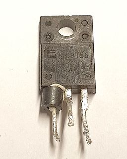
Leistungstransistor im TO-220 Gehäuse
P89T56 K8560
in „Welcher MOSFET ist das?“ · Analoge Elektronik und Schaltungstechnik · · Fotos
-
Bild
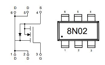
Schaltplan und Gehäusezeichnung eines MOSFETs
D D S 6 5 4 1 D D G 3 8N02
in „Ai Hydra 26HD LED Platinenreperatur Bauteilidentifizierung“ · Mikrocontroller und Digitale Elektronik · · Schaltpläne
-
Bild
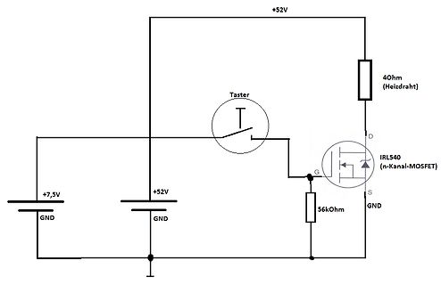
Schaltplan mit MOSFET und Heizdraht
+52V, 40Ohm (Heizdraht), Taster, IRL540 (n-Kanal-MOSFET), D, G, S, GND, +7,5V, 56kOhm
in „Problem mit Mosfet IRL540 an 52V, öffnet nicht mehr“ · Analoge Elektronik und Schaltungstechnik · · Schaltpläne
-
PDF
IR2117_Mosfet_Driver.pdf
phase with input (IR2118) Packages Description The IR2117/IR2118 is a high voltage, high speed power MOSFET and IGBT driver.Proprietary HVIC and latch immune CMOS technologies enable rug- gedized monolithic construction. The logic input is compatible with standard CMOS outputs. The out- put driver features
in „MOSFET Ansteuerung“ · Analoge Elektronik und Schaltungstechnik ·
-
PDF
MOSFET-irfiz34v.pdf
PD - 94053 IRFIZ34V ® HEXFET Power MOSFET l Advanced Process Technology D l Ultra Low On-Resistance V DSS = 60V l Dynamic dv/dt Rating l 175°C Operating Temperature R DS(on) = 28m l Fast Switching G l Fully Avalanche Rated I = 20A l Optimized
in „Frage zur Optokoppler“ · Mikrocontroller und Digitale Elektronik ·
-
PDF
MOSFET_MaWin_1_.pdf
LSP1 T A L 4 DQ1 c a 0 3 2 IRFP450 R R V 85 8 5 m 4 , 3 , 2 R 0 R 0 1 b 4 . c D LSP2
in „Elektronische Wechselstromsicherung“ · Analoge Elektronik und Schaltungstechnik ·
-
Datei
mosfet_optimale_diode_verpolschutz.txt
$ 1 0.000005 10.20027730826997 50 5 50 5e-11 f 240 224 288 224 32 1.5 0.02 172 144 336 144 288 0 7 5 5 0 0 0.5 Drain Voltage g 368 176 368 192 0 0 r 240 224 160 224 0 1000 w 288 208 368 176 0 r 208 304 304 304 0 50 w 304 240 304 304 0 w 208 304 160 224 0 w 144 336 208 304 0 w 288 240 304 240 0 g 464 112 464 128 0 0 172 208 112 208 64 0 7 5 5 0 0 0.5 Drain Voltage r 208 112 304 112 0 50 d 304 112 464 112 2 default r 704 176 800 176 0 50 r 656 192 576 192 0 1000 g 800 208 800 224 0 0 172 800 176 800 128 0 7 5 5 0 0 0.5 Drain Voltage f 656 192 704 192 32 1.5 0.02 w 800 176 848 176 0 w 848 176 848
in „18650 an Handy anschließen, Verpolschutz N Kanal Mosfet“ · Analoge Elektronik und Schaltungstechnik ·
-
PDF
lm5107_MOSFET_Treiber.pdf
HB and HS pins to support high peak currents being drawn from VDD during turn-on of the external MOSFET. 2. To prevent large voltage transients at the drain of the top MOSFET, a low ESR electrolytic capacitor must be connected between MOSFET drain and ground (V ). SS 3. In order to avoid large negative
in „Spannungsversorgung IC 50V auf 12V/5V regeln“ · Analoge Elektronik und Schaltungstechnik ·
-
Bild
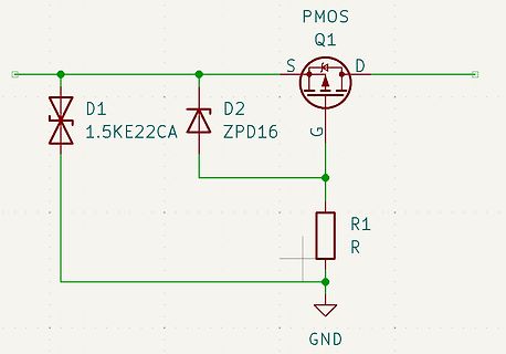
Schaltplan mit PMOS-Transistor und Dioden
PMOS Q1 S D G D1 1.5KE22CA D2 ZPD16 R1 R GND
in „Hilfe beim KiCad-Layout gesucht: 2-Fach Motorsteuerung (KFZ-Bereich)“ · Platinen · · Schaltpläne
-
Bild
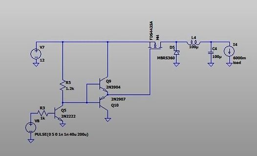
Schaltplan eines DC-DC-Wandlers oder Leistungsschaltkreises
V7 12 M4 FDS443SA D5 MBRS360 L4 100u C4 100u I4 6000m load R5 1.2k Q9 2N3904 Q10 2N2907 R3 1k Q5 2N2222 V8 PULSE(0 5 0 in 40u 200u)
in „Frage zu Push Pull Abwärtswandler“ · Analoge Elektronik und Schaltungstechnik · · Screenshots
-
Bild
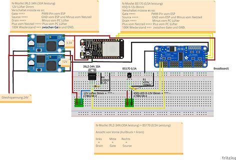
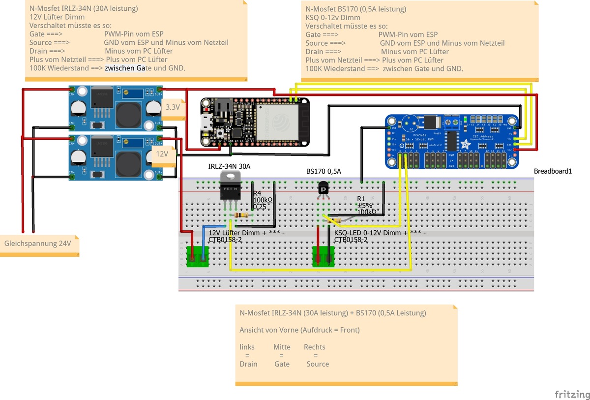
Fritzing-Visualisierung eines MOSFET-Schaltkreises auf Breadboard
N-Mosfet IRLZ-34N (30A leistung) 12V Lüfter Dimm Geschaltet müsste es so: Gate ===> PWM-Pin vom ESP Source ===> GND vom ESP und Minus vom Netzteil Drain ===> Minus vom PC Lüfter Plus vom Netzteil ===> Plus
in „Verständnisfrage bei typischen Schaltungen von μC und gleicher Masse?“ · Mikrocontroller und Digitale Elektronik · · Screenshots
-
Bild
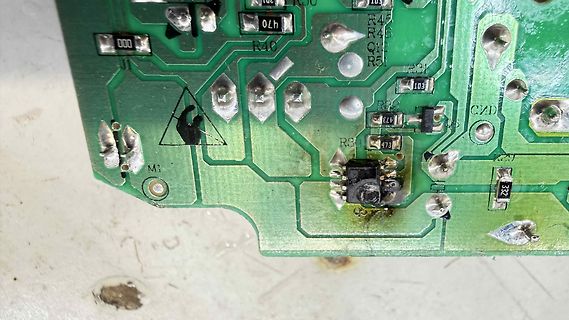
Nahaufnahme einer grünen Leiterplatte mit Bauteilen
000, 470, R47, R46, Q1, R5, 103, R72, 473, R31, СИД, 332, M3
in „Serienfehler Lidl/Parkside X20 Ladegerät?“ · Analoge Elektronik und Schaltungstechnik · · Platinenfotos
-
Bild
Display eines Multi-function Testers T7
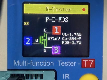
M-Tester P-E-MOS 32 D 1 2 G 671mV Cg=834pF RDS=0,7 S 3 Multi-function Tester - T7 IR
in „H-Brücke mit defektem MOSFET - Bauteil und Ursache bestimmen“ · Analoge Elektronik und Schaltungstechnik · · Fotos