5.5 V, VOUT < 0.4 V 100 185 mA
VIN = 2.4 V, VOUT = 2.15 V 200 385 mA
LOGIC INTERFACE
VEN_H EN logic high threshold VIN > 1.3 V or VOUT > 2.2 V 1.2 V
VEN_L EN logic low threshold VIN > 1.3 V or VOUT > 2.2 V 0.35 0.42 0.45 V
PROTECTION
TSD Thermal shutdown threshold TJ rising 150 °C
Controller Controller TIMING AND MEASUREMENTS: Signal Measurement with Timing and Counter Control LOW POWER AND SYSTEM FLEXIBILITY: Low-Power Technology, Peripheral and Interconnects 8-/12-/16-bit Timer General purpose 8-/12-/16-bit timer/counter Moves data between memories and peripherals without CPU
Controller Controller TIMING AND MEASUREMENTS: Signal Measurement with Timing and Counter Control LOW POWER AND SYSTEM FLEXIBILITY: Low-Power Technology, Peripheral and Interconnects 8-/12-/16-bit Timer General purpose 8-/12-/16-bit timer/counter Moves data between memories and peripherals without CPU
einen besseren Ersatz des TS974 Rail-to-rail output voltage swing ±2.4 V at VCC = ±2.5 V Very low noise level: 4 nV/√Hz 250 fA/√Hz Ultra low distortion: 0.003 % High dynamic features: 12 MHz, 4 V/µs Hätte gerne eine obere Grenzfrequenz von ca. 50kHz bei einer Verstärkung um ca. 750, was eine
Hier bin ich mir aber unsicher wie der Pullup ausgelegt werden soll, damit das Signal vernünftig High oder Low ist. Könnt ihr mir hier direkt sagen, welche Methode vielversprechender ist oder habt ihr noch weitere gute Ideen, die mir hier weiterhelfen. Vielen Dank
Flankenabständen ein verarbeitbare Signal. Davor ist die Zeitkonstante, bis das Signal wieder auf High ist, zu kurz, um es auswerten zu können. Ich bin dann erst wieder bei 50% obwohl der nächste Impuls kommt und das Signal wieder auf LOW zieht.
STOP t 1.3 Fs and START Condition BUF Hold Time (Repeated) START t (Note 9) 0.6 Fs Condition HD:STA Low Period of SCL Clock tLOW 1.3 Fs High Period of SCL Clock t 0.6 Fs HIGH Data Hold Time HD:DAT (Notes 10, 11) 0 0.9 Fs Data Setup Time SU:DAT (Note 12) 100 ns Setup Time for a Repeated t 0.6 Fs START
reduce the output ripple voltage, several standard electrolytic capacitors can be paralleled, or a higher- grade capacitor can be used. Such capacitors are often called high-frequency, low-inductance, or low-ESR. These reduce the output ripple to 10 mV or 20 mV. However, when operating in the continuous
Current converters that maintain high efficiency over a wide Logic Controlled Shutdown to 15 A range of output current. They operate from a supply Low V CESAT Switch: 310mV at 2A Typical voltage as low as 2V and feature automatic shifting
19-0191; Rev 2; 12/02 EVALUATIONK I AVAILABLE -5V/-12V/-15V or Adjustable, High-Efficiency, Low I Inverting DC-to-DC Controllers Q M General Description Features A The MAX774/MAX775/MAX776 inverting switching 85% Efficiency for 5mA to 1A Load Currents regulators deliver high efficiency
5.0 5.5 V Ta=20°C - - 5.7 V Supply Voltage for LCD VDD-V O Ta=25°C 4.2 4.35 4.5 V Ta=70°C 3.5 - - V High-level Input VIH - 0.7 x VDD - VDD V Low-level Input VIL - VSS - 0.6 V High-level Output V OH - 3.9 - VDD V Low-level Output V OL - 0 - 0.4 V Supply Current DD V DD= 5.0V 0.3 1.6 3.3 mA 10. Optical Characteristics
Transistor in Sättigung, was auch durch das berechnete Verhältnis I_C / I_B bestätigt wird. • I_C, U_µC_High und U_µC_Low bleiben auch gleich wenn R_2 entfernt wird (ausgenommen bei U_S > U_e), wie erwartet. • R2 darf bei gegebendem R_1 sein Minimum nicht unterschreiten, da sonst die Schaltgrenze U_S über
LT1305 Micropower High Power DC/DC Converter with Low-Battery Detector U F EA U T RE S DESCRIPTIO ® 5V at 400mA from2V Input The LT 1305 is a micropower step-up DC/DC converter Supply Voltage As Low As 1.8V thatusesBurstMode
Current converters that maintain high efficiency over a wide Logic Controlled Shutdown to 15 A range of output current. They operate from a supply Low V CESAT Switch: 310mV at 2A Typical voltage as low as 2V and feature automatic shifting
START and STOP conditions Both data and clock lines remain HIGH when the bus is not busy. A HIGH-to-LOW transition of the data line while the clock is HIGH is defined as the START condition (S). A LOW-to-HIGH transition of the data line while the clock is HIGH is
Dauersignal (+5V) am Eingang 1 (E1) soll nach 10sec (t1) Verzögerung den Ausgang (A) für 30sec (t2) von Low (0V) auf High (5V) schalten. 2. Der Ausgang (A) muss bei Anlegen, Wegfall oder Unterbrechung der Versorgungsspannung sicher auf Low gesetzt werden/sein. 3. Der Ausgang (A) sollte durch einen Impuls
> 3. Der Ausgang (A) sollte durch einen Impuls (5V) an Eingang 2 (E2) - > unabhängig ob E1 noch High ist - auf Low gesetzt werden. Das ist aber ne neue Salamischeibe. Kommen noch mehr?
immer noch unklar, ob der "USU-RS232" ein echtes RS-232 macht (dann sind die Pegel invertiert, also low bei Idle). Falls er einen Sub-D-9 hat, ist das sehr wahrscheinlich. Zur Überprüfung könntest du den TX vom Adapter auf dem Oszi anschauen, und Daten vom PC her senden, und das Oszillogramm vergleichen
gemessen, dass der ESP sendet (Bild vom 11.2.). - Er sieht 900µs Bitzeit, also ca. 115k. - Idle is high, wie man das erwarten würde. - Der Tastkopf ist falsch eingestellt. Das Bild zeigt 330mV anstatt 3.3V high. - Am Ausgang des USB-RS232-Wandlers misst er (am 11.2. 10:05) dass Idle low ist, also ein
Audio-Verarbeitung besonders in den Vordergrund zu stellen sucht: [c] The NAU88L21CYG is an ultra-low power high-performance audio codec that supports both analog and digital audio functions. It includes one I2S/ PCM interface, one set of digital microphone interfaces, one digital mixer, two high-quality
stereo class-G headphone amplifier. . . . NAU88L21CYG Market Advantages Conventional codecs without low pass filters will cause delay/ high latency during audio data transmission on critical events, especially in the real-time stream processing applications. It will cause a mismatch between audio and
MR), and six buffered outputs (Q0 to Q5). Information on D0 to D5 is transferred to Q0 to Q5 on the LOW-to-HIGH transition of CP if MR is HIGH. When LOW, MR resets all flip-flops (Q0 to Q5 = LOW) independent of CP and D0 to D5. It operates over a recommended V DD power supply range of 3 V to 15 V referenced
transfer 7.1.1 START and STOP conditions Both data and clock lines remain HIGH when the bus is not busy. A HIGH-to-LOW transition of the data line while the clock is HIGH is defined as the START condition (S). A LOW-to-HIGH transition of the data line while the clock is HIGH is
kW (8/20 μs) • Stand-off voltage range from 5 V to 188 V • Unidirectional and bidirectional types • Low leakage current: 0.2 μA at 25 °C and 1 μA at 85 °C K • Operating Tjmax: 150 °C • High power capability at T max.: up to 350 W (10/1000 µs) j A • Lead finishing: matte tin plating Bidirectional Unidirectional
Jetzt mal mit LA: D0 SCK not D1 SO D2 SI Wie gesagt zu beachten ist das SI durch die Schaltung Low wird wenn SO High ist. Ich habe in Idle 3 mal markiert was ich mit der Pulsweite meine. Außerdem habe ich mal eine Reihe aufgenommen, die zeigt was passiert, wenn ich einmal die Plus taste drücke
zu werden, dass eine Seite die Datenleitung auf low zieht und danach die Übertragung von 8 Bit mit auf der langsameren Frequenz stattfindet (SPI, Datenübernahme bei steigender CLK Flanke). Nachdem 8 Bit in eine Richtung übertragen wurden, wartet die
duty cycle 33% .frequency_hz = 38000, // 38 KHz .flags.polarity_active_low = false, // carrier should be modulated to high level .always_on = true, // If set, the carrier can always exist even there's not transfer undergoing }; // modulate
1 1 1 0 2 1 1 3 (Highest) 47 4164G–SCR–07/06 A low-priority interrupt can be interrupted by a high priority interrupt, but not by another low-priority interrupt. A high-priority interrupt can’t be interrupted by any other
1MHz,measuredtoGND, 60 pF code=0x80 Common-ModeLeakage ICM VA=V BV W 1 nA DIGITALINPUTS InputLogicHigh(SDAandSCL) V 0.7×V V +0.5V V IH DD DD InputLogicLow(SDAandSCL) VIL −0.5 +0.3×VDD V InputLogicHigh(AD0andAD1) V V =5V 2.4 V V IH DD DD InputLogicLow(AD0andAD1) VIL VDD5V 0 0.8 V InputLogicHigh V V =3V
gemacht Ja, weil die meisten USB-Serial-Adapter wohl FullSpeed-Geräte sind bräuchtest du einen HighSpeed Hub welcher für alle 8 Ports Transaction Translators hat. Oder USB-Serial-Adapter die direkt USB HighSpeed können. Nur so kann man die volle Datenrate des HighSpeed Ports vom PC nutzen. Könnte
Davon 2 und irgendein HighSpeed Hub, fertig. Leider nicht ganz günstig.
) and biopotential (BioZ) analog front end (AFE) for wearable applications. The MAX86178 offers high performance for wellness and clinical applications with low power for long battery life [/c] Nun steht dafür ein Evaluationsboard zur Verfügung, das die Sensordaten per Bluetooth oder USB ansprechbar
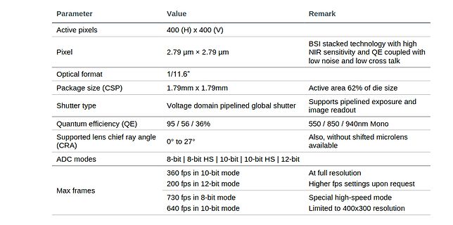
Value Remark
Active pixels 400 (H) x 400 (V)
Pixel 2.79 µm x 2.79 µm BSI stacked technology with high NIR sensitivity and QE coupled with low noise and low cross talk
Optical format 1/11.6"
Package size (CSP) 1.79mm x 1.79mm Active area 62% of die size
Shutter type Voltage domain pipelined global shutter
probieren ob der Ausgangsstrom wieder unterm Limit bleibt? Constant-Current? ...? Soll das Ding High-Side oder Low-Side eingesetzt werden? Wenn High-Side - bist Du Dir ganz sicher dass es High-Side sein muss und es nicht auch Low-Side ginge?
Komponenten einen defekt aufweisen oder wo ich nachher probleme in meiner Leitung habe. Ja so ein High-Side-Switch / Low-Side-Switch ist ja auch mit "smarten" funktionen ausgestattet auch eine "protection" IC deswegen habe ich es darunter Publiziert. Es kann auch ein Low-Side-Switch sein es muss
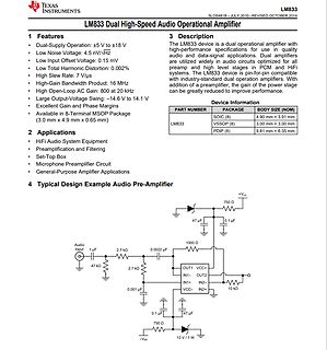
Texas Instruments LM833 Dual High-Speed Audio Operational Amplifier SLOS481B-JULY 2010-REVISED OCTOBER 2014 1 Features Dual-Supply Operation: ±5 V to ±18 V Low Noise Voltage: 4.5 nV/√Hz Low Input Offset Voltage: 0.15 mV Low Total Harmonic Distortion: 0.002% High Slew Rate: 7 V/µs High-Gain Bandwidth Product: 16 MHz High Open-Loop AC Gain: 800 at 20 kHz Large Output-Voltage Swing: -14.6 V to 14.1 V Excellent Gain and Phase Margins Available in 8-Terminal MSOP
Tolerance: J (±5%); K (±10%); M (±20%) All dimensions are in mm. Note 1: If the working voltage (V) is lower than the rated voltage (V ), the capacitoR may work at higher dv/dt. In this case the maximum value allowed is obtained multiplying the above value (see table dv/dt) with the ratio V /V. The pulse
ein Programm bräuchtest Du, um den Adressraum bis 1088 KByte anzusprechen. (von 1024 bis 1088 ist High Memory Area im Extended Memory.) Quelle: 9783423503013 "MS DOS von A bis Z", Seite 157 ciao gustav
schrieb im Beitrag #7823100: > So wie es aussieht, darf man bei SDRAM den Takt auch anhalten (CKE = > low). Im Datenblatt CKE = LOW ist NICHT das Gleiche wie den Takt selber anhalten (CLK)! Den der Takt treibt ja sämtliche State Machines, Zähler etc. im SDRAM! Bei echtem, old school SDRAM kann man
links rum adc AL, AH brcc MPaX ;Kein Überlauf ldi AH, 255 out PWM1, AH com AL out PWM2, AL ldi AL, LOW(MPb) sts PWMAdrl, AL ldi AL, HIGH(MPb) sts PWMAdrh, AL ret MPa2: ;rechts rum sbc AL, AH brcc MPaX ;Kein Überlauf ldi AH, 0 out PWM1, AH com AL sts PWM5, AL ldi AL, LOW(MPj) sts PWMAdrl, AL ldi AL, HIGH
Time SU:STO 2.6 — — µs Data Hold Time HD:DAT 0 — — µs Data Setup Time SU:DAT 1.3 — — µs Detect Clock Low Timeout t 25 — — ms TIMEOUT Clock Low Period LOW 1.3 — — µs Clock High Period HIGH 2.6 — 503 µs Note: 1.The minimum SMBus frequency is limited by the maximum Clock High Period requirement of the SMBus
Beitrag fällt. Thomas F. schrieb im Beitrag #7824780: > Beitrag "Re: Arduino Inputs willkürlich HIGH & LOW trotz Pullup" Den Vorteil bzw. entstehende Schutz dieser Schaltung ist mir leider nicht ganz ersichtlich, aber vielleicht kannst du ihn mir kurz erklären? Das ist ein Spannungsteiler der direkt

 Bild

 Bild
 Bild
 Bild
 Bild
 Bild